Cite this: Phys. Chem. Chem. Phys ., 2011, 13, 13552–13557
On the formation of anisotropic gold nanoparticles by sputtering onto a nitrile functionalised ionic liquid w
Heberton Wender,
aPedro Migowski,
bAdriano F. Feil,
aLuciane F. de Oliveira,
bcMartin H. G. Prechtl,
bRafael Leal,
bGiovanna Machado,
dSergio R. Teixeira*
aand Jairton Dupont*
bReceived 3rd May 2011, Accepted 15th June 2011 DOI: 10.1039/c1cp21406c
Sputtering deposition of gold onto the 1-(butyronitrile)-3-methylimidazolium
bis(trifluoromethylsulfonyl)imide (BCN)MIN(Tf)
2ionic liquid (IL) has generated colloidal and stable gold nanospheres (AuNS) and gold nanodisks (AuND) in a bimodal size distribution.
Upon increasing the sputtering discharge voltage, three distinct phenomena were observed:
(i) the mean diameter of both AuNS and AuND decreased; (ii) the population with lower diameters increased and (iii) the formation of AuND disappeared at voltages higher than 340 V.
By dissolving the colloidal gold nanoparticles (AuNPs) in isopropanol and dropping the product onto carbon-coated Cu grids, 2D and 3D superlattices tended to be formed, as observed by transmission electron microscopy (TEM). Therefore, the formation of AuND is probably related to a strong interaction between sputtered Au atoms of low kinetic energy and the nitrile groups orientated to the vacuum phase of the IL surface, which drives the preferential anisotropic lateral growth.
1. Introduction
Physical vapour deposition (PVD) of metals in low vapour pressure liquids has recently emerged as a versatile and simple method for the generation of nanoparticles (NPs) in solution.
1–5Due to the high purity of these NPs, they are suitable for a variety of applications such as magnetic fluids,
1nonlinear optics, biomedicine and catalysis.
6Among all employed PVD methods to prepare colloidal NPs, sputtering deposition onto ionic liquids (ILs) has several advantages since its versatility allows a good control over the size and size distribution of the NPs,
7,8which is of great importance for special applications.
9–14Moreover, in the case of sputtering deposition onto ILs, very stable spherical NPs are easily prepared by simply adjusting
the physical parameters during the sputtering process, allowing for control of the NPs size and size distribution without the addition of extra stabilisers.
15However, the factors that govern NPs growth in the sputtering process are still unclear.
In fact, recent reports suggest that NPs nucleate and grow on the IL surfaces,
16as also observed for sputtering onto castor oil.
17Thus, the chemical configuration of the IL surface and the energy of the sputtered atoms must play crucial roles in the formation of NPs.
Moreover, the surface of the ILs could be easily tuned just by changing the anion identity and cation substituents,
18thus propitiating interesting local environments for NP growth and, perhaps, for anisotropic NP formation. Indeed, the IL surface organisation always involves two interconnected aspects: (i) the surface composition and (ii) the surface ion orientation. In the case of non-functionalised ILs, both cations and anions are present in the surface region of pure imidazolium- based ILs,
19–21with the alkyl chains projected into the gas phase.
22The anion composition is another parameter that greatly affects the outmost layers of the ILs. Anions with long perfluorinated chains tend to populate the vacuum/IL interface with the long alkyl chains within the first few Angstroms of the surface.
18,19Therefore, one might expect that introducing functional groups on the cation of the ILs would allow for rationally controlling the generation of NPs by means of surface composition modification.
In the case of functionalised ILs, the surface composition is so far unknown.
23In such systems, it can be expected that the
aLaborato´rio de Filmes Finos e Fabricac¸a˜o de Nanoestruturas (L3Fnano), Instituto de Fı´sica, Av. Bento Gonc¸alves 9500, P.O. Box 15051, 91501-970, UFRGS, Porto Alegre, Brazil.
E-mail: durao@if.ufrgs.br
bLaborato´rio de Cata´lise Molecular (LAMOCA), Instituto de Quı´mica, Av. Bento Gonc¸alves 9500, P.O. Box 15003, 91501-970, UFRGS, Porto Alegre, Brazil. E-mail: jairton.dupont@ufrgs.br
cLaborato´rio Nacional de Luz Sı´ncrotron (LNLS), Campinas, Brazil
dCentro de Tecnologias Estrate´gica do Nordeste (CETENE), Postal Code 50.740-540, Recife, Brazil
wElectronic supplementary information (ESI) available: Detailed experimental condition; SAXS acquisition data and analysis; UV-Vis of ILs after sputtering of Au at different discharge voltages, Fig. S1;
and SAXS size distribution of AuNPs obtained by sputtering at 340 V for 150 s onto the EMIN(Tf)2ionic liquid, Fig. S2. See DOI: 10.1039/
c1cp21406c
PCCP Dynamic Article Links
www.rsc.org/pccp PAPER
surface composition depends on the polarity of the functional group. Weakly polar groups will probably follow the same trend observed for ILs with solely aliphatic side-chains.
However, in the case of polar groups, the functional groups might be oriented to the gas phase or fold to interact with the charged moieties of the IL. Therefore, it should be expected that the nitrile-functionalised IL surface might be different from ILs containing solely aliphatic side-chains. For the nitrile functionality, at least two possibilities for the surface chemical configuration can be depicted: (i) due to the dipolar moment of the nitrile, the butyronitrile side chain might fold into the ionic region of the surface to form hydrogen bonds and/or dipole–
dipole interactions, Fig. 1a; (ii) the nitrile functionalised side chain will orient itself to the vacuum/IL interface, Fig. 1b.
We report herein that the use of a nitrile functionalised, 1-(butyronitrile)-3-methylimidazolium bis(trifluoromethyl- sulfonyl)imide [(BCN)MIN(Tf)
2] IL dramatically changes the interfacial composition of the vacuum/IL and allows the synthesis of colloidal gold nanodisks (AuND) and gold nano- spheres (AuNS). Moreover, we show that, depending on the sputtering conditions, AuNS and/or AuND were produced in the (BCN)MIN(Tf)
2IL. The obtained nanostructures were characterised and compared with those produced in non-functionalised ILs and a mechanism related to the surface composition of the ILs was proposed.
2. Experimental section
2.1 Preparation of the colloids
Gold nanoparticles (AuNPs) were prepared by a sputtering deposition technique. The (BCN)MIN(Tf)
2was synthesised as described in the literature,
24and degassed for approximately 3 h at 298 K under vacuum prior to being introduced into the sputter chamber as a liquid substrate for sputtering deposition of gold. Deposition was performed for 150 s in a MED 020 (Bal-Tech) in the sputter mode with discharge voltages from 275 to 410 V (powers from 2 to 45 W), under an argon pressure of 2 Pa at room temperature. In each deposition, a mass of 1.2 g of (BCN)MIN(Tf)
2was placed on a Petri plate (3 cm in diameter) and horizontally set in the sputter coater. The liquid surface was located at a distance of 50 mm from the gold target (99.99% in purity).
2.2 Characterisation
The structure, shape, size and size distribution of the Au NPs were investigated using a JEOL JEM1200 transmission
electron microscope (TEM) operating at 80 keV, a FEI Tecnai 20 high resolution transmission electron microscope (HRTEM) coupled with a Tomography Xplore3D module operating at 200 KeV and small angle X-ray scattering (SAXS) recorded at the SAXS1 beam line at the Brazilian Synchrotron Light Laboratory (LNLS). More details for the SAXS experiments can be found in the ESI
wand elsewhere.
17UV-Vis absorption spectroscopy was measured on a Varian Cary 100 spectro- photometer using 1 mm quartz cuvettes.
The sample topography and mean height were characterised
ex situin a Nanoscope IIIa (Digital Instruments) scanning force microscope (SFM) in Tapping Modet, with Nano- sensorst CNT-NHC tips (with nominal carbon nanotube radius
o2.1 nm and length
o750 nm).
For more experimental details, see the ESI.
w3. Results and discussion
3.1 General results
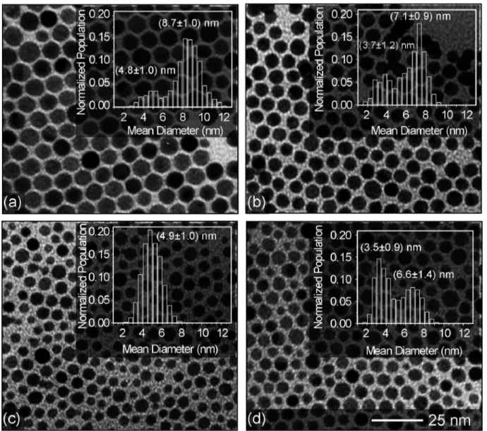
Fig. 2 shows representative TEM images and histograms of the samples sputter deposited at different discharge voltages onto (BCN)MIN(Tf)
2. As can be seen in the histo- grams, most samples possessed bimodal size distributions, and the AuNPs population with smaller diameters was more pronounced as the discharge voltage increased. Also, the mean diameter of both populations decreased as the discharge voltages increased. The bigger particles having a diameter of 8.7 nm obtained at 275 V, Fig. 2a, diminished to 6.6 nm when deposited at 365 V, Fig. 2d. A similar behaviour could also be observed for the smaller particles, which decreased their mean diameter from 4.8 nm to 3.5 nm as the discharge voltage increased. However, as an exception to this behaviour, a monomodal size distribution was observed when a 340 V sputtering discharge was used during the deposition. This result could be interpreted as an inter- mediate case where both populations of NPs possess equal weights on the size distribution, forming a single distribution population.
As shown in Fig. 2, 2D superlattices of nanoparticles tended to be formed by dropping the colloids on the carbon-coated copper grids (for TEM measurement). It can be seen that an apparent disorganisation was the result of increasing the amount of small NPs. Additionally, the distance between particles also increased as the disorder of the lattices increased.
Fig. 3a and b show a 3D superlattice, which was spontaneously
formed on the carbon-coated Cu grid. These superlattices were
Fig. 1 Possible behaviour for surface configuration and ions orientation on the (BNC)MIN(Tf)2IL. (a) Nitrile functional groups interacting with cationic regions and (b) nitrile functional groups oriented out of the IL surface.highly organised in hexagonal packages consisting of two or more overlapping planes that presented a certain twist from one to another, similar to previous reports.
25Note that in both cases (Fig. 2 and 3), the AuNPs were well-organised in hexagonal packages, where each plane was composed of an extremely organised AuNPs layer. The energy dispersive spectroscopy (EDS) spectrum (Fig. 3a inset) showed the presence of Au atoms on the sputtered samples, and the high resolution TEM (HRTEM) image (Fig. 3c) confirmed the presence of crystalline AuNPs with a
d-spacing of 2.4 A˚corresponding to the (111) planes characteristic of the fcc structure.
The UV-Vis absorption spectra of the Au colloids show peaks within the range 525–560 nm due to the dipole surface plasmon resonance peak (SPR) of AuNPs
26(see Fig. S1 of the ESI
w). The sample sputtered at 300 V was the only case where the absorption spectrum had two bands, one centred at 560 nm and the other at 720 nm. Theoretically, for the same liquid matrix, the SPR will depend on the particle size, size distri- bution, form factor and on the distance between particles.
27Therefore, the peak observed at 720 nm probably arose from the considerable proximity between particles as corroborated by the SAXS measurements (see below).
Fig. 2 TEM images of Au NPs deposited by sputtering of an Au target for 150 s onto (BCN)MIN(Tf)2with discharge voltages of (a) 275 V, (b) 300 V, (c) 340 V and (d) 365 V. All charts have the same scale bar. The inset shows the respective histogram.
Fig. 3 NPs agglomeration observed in samples synthesised by sputtering at 300 V for 150 s. (a) and (b) TEM images and (c) representative HRTEM image.
Thus, SAXS measurements were conducted on the colloidal samples in order to investigate size distributions, form factors and the correlations between AuNPs. Depending on the sample, for simulation and accurate fitting of the scattering curves, it was crucial to consider two or three major contributions and a hard sphere structure factor.
28Surprisingly, it was necessary to include a non-spherical form factor,
29that is, an oblate ellipsoid, to fit some scattering curves. The theoretical scattering intensities of spheroids and ellipsoids used to fit the scattering curves are displayed in eqn (1) and (2), respectively. In these equations,
Rrepresents the sphere radius,
DZthe scattering length density difference between the particles and the matrix,
Qthe scattering vector,
Rethe radius of the ellipsoid rotational axes and
Wthe ratio between radius of the semi-principle axes and the equatorial axis of the ellipsoid. More details on SAXS analysis and funda- mental equations are described elsewhere.
29,30The SAXS curves of the IL containing AuNPs prepared with different discharge voltages are shown in Fig. 4.
ISphereðQ;RÞ ¼
4
3
pR3DZ3sin
QRQRcos
QR ðQRÞ2!2
ð1Þ
IEllipsoidðQ;Re;WÞ ¼
4 3
pR3e2
Z p=2
0
k2ðQ;Re ffiffiffiffiffiffiffiffiffiffiffiffiffiffiffiffiffiffiffiffiffiffiffiffiffiffiffiffiffiffiffiffiffiffi W2
cos
2yþsin
2yp Þ
dy
ð2Þ
As can be seen, the simulation of the scattering curves revealed that the large size NPs populations were, in fact, composed of two contributions: one with AuNS and another with ellipsoids (AuND). The AuND population decreased with increased discharge voltage, and after 340 V only AuNS completely fitted the SAXS data (see details in Table 1). A decrease in the mean diameters of the AuNPs with an increase in the discharge voltage was also observed by SAXS, corroborating the findings from the TEM analysis.
The experimental SAXS curves (Fig. 4a) clearly show the presence of a strong structure factor (see ESI
wfor details), which was highest for the sample sputtered at 300 V and decreased with increased discharge voltage. The strong correlation between NPs in the sample sputtered at 300 V can explain the second absorption band observed in the UV-Vis analysis. In addition, SAXS analysis confirmed that the size distributions of the NPs were bimodal, with one having mean diameters in the range of 3–4 nm (spheres only) and the other around 7–8 nm (spheres and/or ellipsoids).
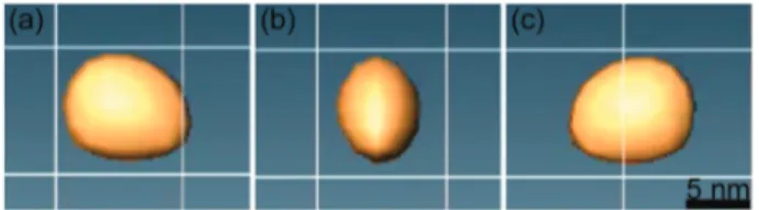
TEM tomography of the sample sputtered at 300 V (Fig. 5;
video is available in the ESI
w) showed the presence of AuND of around 8 nm in diameter and with a thickness of
B3 nm,corroborating the SAXS findings. The superlattice self- organisation and AuNPs height distribution were confirmed by scanning force microscopy (SFM) analysis of AuNPs sputtered at 300 V (Fig. 6). The measurement of approx- imately 150 particles showed that the height distribution of the AuNPs was bimodal, with mean height values of 1.3 0.8 nm and 2.6 0.4 nm (Fig. 6c). SFM also showed that the agglomerated regions presented two or three planes of
Fig. 4 SAXS data of AuNS and AuND sputtered on (BCN)MIN(Tf)2for 150 s with discharge voltages of 275, 300, 340, 365, and 410 V (a). In (b) the best fitted curve of the sample sputter deposited at 300 V is shown representatively. Inset in (b) shows the size distribution of the spheres and disks obtained by adjusting the scattering curve. The structure factor used to fit displays a hard sphere repulsion radius (RHS) and volume fraction (fp) of 4.3 and 0.5, respectively. Also, a mass fractal of dimension 2.8 was used for the fit.Table 1 SAXS fitting parameters (form, size and size distributions) of the colloidal AuNPs obtained by sputtering onto (BCN)MIN(Tf)2for 150 s at different discharge voltages
Voltage/V Form factor Diameter/nm Height/nm
Standard deviation (%)
275 Sphere 4.0 4.0 33.0
Ellipsoid 8.2 5.4 26.6
300 Sphere 6.2 6.2 6.0
Ellipsoid 7.8 2.5 2.0
Sphere 3.4 3.4 2.0
340 Sphere 6.6 6.6 17.6
Ellipsoid 7.8 3.9 39.5
Sphere 3.0 3.0 12
365 Sphere 9.6 9.6 105.4
Sphere 5.4 5.4 52.2
410 Sphere 5.1 5.1 17.6
agglomerated NPs (Fig. 6a and b) as observed by TEM analysis.
3.2 Disk-shaped NPs formation mechanism
The mechanism of thin films growth onto a liquid substrate has been intensely studied in a number of recent investigations.
31–37These studies showed that the metal film formation process onto liquid surfaces proceeds through the following stages:
nucleation, growth of compact atomic clusters, aggregation of branched islands, and finally, the formation of continuous films.
35In addition, the deposited atoms, compact clusters, and branched islands are extremely mobile on the liquid surface, which indicates that the interaction between the metal film and the liquid substrate in the tangent direction is very small, as compared with a solid substrate.
37We observed that Au deposition onto (BCN)MIN(Tf)
2only forms thin films when very low sputtering rates and relatively low discharge voltages are used; otherwise, NPs are produced. In fact, AuNP growth on the surface of the ILs seemed to stop when forming compact clusters followed by the diffusion of the NPs into the liquid bulk phase. This behaviour clearly indicates that the liquid–metal cluster inter- action on the IL surface is very different from that previously observed for silicone oil.
17Thus, modulating the interactions between the incoming gaseous Au atoms and surface composition of the ILs would lead to control of the shape and size of the NPs. In fact, it was shown that the anion content on the IL surface changes the way in which Au atoms interact
with the IL.
16In addition, the energy of the incoming atoms is another important factor in the interaction of the surface and the arriving atoms. More specifically, it was demonstrated that ILs with similar average surface composition generated spherical NPs with similar size distributions, while surfaces enriched with anions, especially the ones derived of the tris-pentafluoroethyl-trifluorophosphate (FAP) anion, generated bigger NPs.
16Therefore, to infer about the growth mechanism of NPs through sputtering, the interactions between the evaporated Au atoms and the surface of the ILs must be discussed.
For AuNPs growth behaviour in the (BCN)MIN(Tf)
2, two distinct liquid surface configurations have to be considered, as discussed earlier. The nitrile group might induce the folding of the side chain, as in Fig. 1a, and the outmost layer of the surface will be rich with charged species, resembling the surface composition of 1-ethyl-3-methylimidazolium bis(trifluoromethylsulfonyl)imide [EMIN(Tf)
2]. However, when Au was sputtered at 340 V onto the EMIN(Tf)
2, only spherical AuNPs of 5.2 (s = 1.0) nm in diameter were formed (Fig. S2, ESI
w) as already observed earlier.
38,39Therefore, these results indicate that the surface composition of the (BCN)MIN(Tf)
2differs from the short alkyl chain ILs.
Moreover, the surface configuration of the nitrile functionalised IL is probably comparable to the long alkyl chain ILs, with the nitrile groups pointing to the vacuum, as in Fig. 1b.
Assuming that the nitrile groups are located on the most external position of the surface, a strong interaction with the incoming Au atoms and the nitrogen of the nitriles is expected.
The coordination of the sputtered Au atoms and/or clusters significantly modifies the manner of AuNPs growth in comparison to the 1-n-butyl-3-methylimidazolium (BMI) cation based ILs.
16The Au atoms coordination diminishes the diffusivity of the atoms and, due to the strong interaction with the surface, propitiates a preferential 2D growth to form AuND.
The energy of the sputtered atoms is also a crucial parameter of the NPs growth mechanism. The small AuNS population increased when the discharge voltages increased and the AuND population decreased. At 410 V (110 mA), AuND were not observed, as indicated in the SAXS analysis.
The increase in the acceleration voltage of the Ar
+ions enhanced the average kinetic energy of the sputtered Au atoms. As the molecular arrangement of the surface of the IL gradually changes until the bulk conformation, the environment in which the AuNPs grow will change dramatically depending on the depth to which the sputtered atoms penetrate into the IL surface. Therefore, a threshold energy for the sputtering atoms which changes the chemical environment where the atoms start NPs growth must exist. Moreover, the sputtered atoms are not isoenergetic, but their energies are in a Boltzmann distribution.
40Increasing the discharge voltage of the sputtering process will increase the average translational energy of the sputtered atoms as well as the fraction of Au atoms that are above the threshold energy for AuNS growth.
This explains the increase in the small AuNS population with increasing voltage in the sputtering process. Therefore, the growth mechanism of the Au in the (BCN)MIN(Tf)
2always involves two interconnected parameters: the conformation of
Fig. 5 TEM tomography images (video available in the ESIw) of aselected AuNP sputtered onto (BCN)MIN(Tf)2at a discharge voltage of 300 V for 150 s. From (a) to (c) the particle is gyrating to the left.
Fig. 6 SFM representative image of NPs sputtered with a discharge voltage of 300 V for 150 s, presented in (a) a 3D image, (b) a phase image of the assembled regions and (c) a height histogram after a count of approximately 150 particles.
the molecular species of the IL surface and the energy of the sputtered atoms. When Au atoms are sputtered with low average kinetic energy, the atoms tend to interact more with the coordinating nitrile groups, forming AuND. The disks were formed by a preferential 2D growth due to a strong interaction between the Au atoms and the butyronitrile side chain in the more external regions of the IL surface, while AuNS were formed by a preferential 3D growth due to anion–gold interactions in the more internal region of the IL surface, as observed with non-functionalised ILs.
16Conclusions
In summary, the sputter deposition of Au onto (BCN)MI N(Tf)
2generates both AuND and AuNS. Controlling the physical parameters of sputtering enables colloidal NPs of different sizes, size distributions, and shapes to be produced without the use of any external stabilising agents. The unexpected formation of AuND is related to the strong interaction between the Au atoms and the nitrile groups of the IL surface.
This coordination of Au atoms drives the lateral growth of the NPs and also indicates that the nitrile functional groups are oriented to the vacuum phase. Moreover, after dropping this highly nanostructured IL solution onto a substrate, both 2D and 3D superlattices of AuNPs are formed in well-organised hexagonal packages. The Au atoms with sufficient energy to penetrate deeply into the IL surface will interact loosely with the outermost nitrile groups, and AuNPs growth occur in a chemical environment that favours the formation of AuNS.
The population of AuND is dependent on the discharge voltage employed and disappears at voltages higher than 340 V. These findings open up a new way to design experiments to produce NPs with unusual shapes and sizes. Moreover, a simple change in surface composition of functionalised ILs might yield new unexpected anisotropic NPs whose synthesis is not possible with classical colloidal methods. The composition of the ILs in the liquid/vacuum interface is an important parameter and more studies on the surface of functionalised ILs must be done in order to better understand the phenomena of NPs growth obtained by PVD of metals.
Acknowledgements
Thanks are due to LNLS for the SAXS1 beam line and CME-UFRGS and CETENE for the sputtering machine and TEM and HRTEM microscopes.
Notes and references
1 M. Wagener and B. Gunther,J. Magn. Magn. Mater., 1999,201, 41–44.
2 K. Richter, A. Birkner and A.-V. Mudring,Angew. Chem., Int. Ed., 2010,49, 2431–2435.
3 X. Zhou, Q. Wei, K. Sun and L. Wang,Appl. Phys. Lett., 2009, 94, 133107.
4 T. Torimoto, K. Okazaki, T. Kiyama, K. Hirahara, N. Tanaka and S. Kuwabata,Appl. Phys. Lett., 2006,89, 243117.
5 H. Wender, M. L. Andreazza, R. R. B. Correia, S. R. Teixeira and J. Dupont,Nanoscale, 2011,3, 1240–1245.
6 M. D. Hughes, Y. J. Xu, P. Jenkins, P. McMorn, P. Landon, D. I. Enache, A. F. Carley, G. A. Attard, G. J. Hutchings, F. King,
E. H. Stitt, P. Johnston, K. Griffin and C. J. Kiely,Nature, 2005, 437, 1132–1135.
7 J. Dupont and J. D. Scholten,Chem. Soc. Rev., 2010,39, 1780–1804.
8 T. Torimoto, T. Tsuda, K. Okazaki and S. Kuwabata, Adv.
Mater., 2010,22, 1196–1221.
9 E. G. Castro, R. V. Salvatierra, W. H. Schreiner, M. M. Oliveira and A. J. G. Zarbin,Chem. Mater., 2010,22, 360–370.
10 M. M. Oliveira, D. Ugarte, D. Zanchet and A. J. G. Zarbin, J. Colloid Interface Sci., 2005,292, 429–435.
11 P. Migowski and J. Dupont,Chem.–Eur. J., 2007,13, 32–39.
12 P. Migowski, D. Zanchet, G. Machado, M. A. Gelesky, S. R. Teixeira and J. Dupont,Phys. Chem. Chem. Phys., 2010, 12, 6826–6833.
13 H. Wender, A. F. Feil, L. B. Diaz, C. S. Ribeiro, G. J. Machado, P. Migowski, D. E. Weibel, J. Dupont and S. R. Teixeira,ACS Appl. Mater. Interfaces, 2011,3(4), 1359–1365.
14 A. F. Feil, P. Migowski, F. R. Scheffer, M. D. Pierozan, R. R. Corsetti, M. Rodrigues, R. P. Pezzi, G. Machado, L. Amaral, S. R. Teixeira, D. E. Weibel and J. Dupont,J. Braz.
Chem. Soc., 2010,21, 1359–1365.
15 T. Kameyama, Y. Ohno, T. Kurimoto, K. Okazaki, T. Uematsu, S. Kuwabata and T. Torimoto,Phys. Chem. Chem. Phys., 2010,12, 1804–1811.
16 H. Wender, L. F. de Oliveira, P. Migowski, A. F. Feil, E. Lissner, M. H. G. Prechtl, S. R. Teixeira and J. Dupont,J. Phys. Chem. C, 2010,114, 11764–11768.
17 H. Wender, L. F. de Oliveira, A. F. Feil, E. Lissner, P. Migowski, M. R. Meneghetti, S. R. Teixeira and J. Dupont,Chem. Commun., 2010,46, 7019–7021.
18 C. Kolbeck, T. Cremer, K. R. J. Lovelock, N. Paape, P. S. Schulz, P. Wasserscheid, F. Maier and H. P. Steinruck,J. Phys. Chem. B, 2009,113, 8682–8688.
19 K. R. J. Lovelock, C. Kolbeck, T. Cremer, N. Paape, P. S. Schulz, P. Wasserscheid, F. Maier and H. P. Steinruck,J. Phys. Chem. B, 2009,113, 2854–2864.
20 S. Caporali, U. Bardi and A. Lavacchi, J. Electron Spectrosc.
Relat. Phenom., 2006,151, 4–8.
21 S. Krischok, M. Eremtchenko, M. Himmerlich, P. Lorenz, J. Uhlig, A. Neumann, R. Ottking, W. J. D. Beenken, O. Hofft, S. Bahr, V. Kempter and J. A. Schaefer,J. Phys. Chem. B, 2007, 111, 4801–4806.
22 S. Rivera-Rubero and S. Baldelli,J. Phys. Chem. B, 2006,110, 4756–4765.
23 C. S. Santos and S. Baldelli,Chem. Soc. Rev., 2010,39, 2136–2145.
24 D. Zhao, Z. Fei, R. Scopelliti and P. J. Dyson,Inorg. Chem., 2004, 43, 2197–2205.
25 J. Fink, C. J. Kiely, D. Bethell and D. J. Schiffrin,Chem. Mater., 1998,10, 922–926.
26 P. Mulvaney,Langmuir, 1996,12, 788–800.
27 K. L. Kelly, E. Coronado, L. L. Zhao and G. C. Schatz,J. Phys.
Chem. B, 2002,107, 668–677.
28 J. K. Percus and G. J. Yevick,Phys. Rev., 1958,110, 1.
29 A. Guinier and G. Fournet, Small-Angle Scattering of X-rays, Wiley, New York, 1955.
30 O. Glatter and O. Kratky, Small Angle X-Ray Scattering, Academic Press, London, 1982.
31 G. X. Ye, Q. R. Zhang, C. M. Feng, H. L. Ge and Z. K. Jiao,Phys.
Rev. B: Condens. Matter, 1996,54, 14754–14757.
32 E. F. Borra, O. Seddiki, R. Angel, D. Eisenstein, P. Hickson, K. R. Seddon and S. P. Worden,Nature, 2007,447, 979–981.
33 S. J. Yu and Y. J. Zhang,Surf. Rev. Lett., 2008,15, 525–530.
34 S. J. Yu, Y. J. Zhang, J. X. Chen and H. L. Ge,Surf. Rev. Lett., 2006,13, 779–784.
35 S. J. Yu, Y. J. Zhang and M. G. Chen,Int. J. Mod. Phys. B, 2010, 24, 997–1005.
36 S. J. Yu, Y. J. Zhang, H. Zhou, P. G. Cai and M. G. Chen,Appl.
Surf. Sci., 2009,256, 909–915.
37 Y. J. Zhang and S. J. Yu, Int. J. Mod. Phys. B, 2009, 23, 3147–3157.
38 Y. Hatakeyama, M. Okamoto, T. Torimoto, S. Kuwabata and K. Nishikawa,J. Phys. Chem. C, 2009,113, 3917–3922.
39 S. Kuwabata, T. Tsuda and T. Torimoto,J. Phys. Chem. Lett., 2010,1, 3177–3188.
40 R. V. Stuart and G. K. Wehner, J. Appl. Phys., 1964, 35, 1819–1824.