Forces from periodic charging of adsorbed molecules
N. Kocić , S. Decurtins, S.-X. Liu, and J. Repp
Citation: The Journal of Chemical Physics 146, 092327 (2017); doi: 10.1063/1.4975607 View online: http://dx.doi.org/10.1063/1.4975607
View Table of Contents: http://aip.scitation.org/toc/jcp/146/9
Published by the American Institute of Physics
Forces from periodic charging of adsorbed molecules
N. Koci´c,
1S. Decurtins,
2S.-X. Liu,
2,a)and J. Repp
1,b)1Institute of Experimental and Applied Physics, University of Regensburg, 93053 Regensburg, Germany
2Departement f¨ur Chemie und Biochemie, Universit¨at Bern, Freiestrasse 3, CH-3012 Bern, Switzerland
(Received 1 November 2016; accepted 20 January 2017; published online 21 February 2017) In a recent publication [N. Koci´c et al., Nano Lett. 15, 4406 (2015)], it was shown that gating of molecular levels in the field of an oscillating tip of an atomic force microscope can enable a periodic charging of individual molecules synchronized to the tip’s oscillatory motion. Here we discuss further implications of such measurements, namely, how the force difference associated with the single- electron charging manifests itself in atomic force microscopy images and how it can be detected as a function of tip-sample distance. Moreover, we discuss how the critical voltage for the charge- state transition depends on distance and how that relates to the local contact potential difference.
These measurements allow also for an estimate of the absolute tip-sample distance. Published by AIP Publishing. [http://dx.doi.org/10.1063/1.4975607]
I. GENERAL INTRODUCTION
Experiments in the field of molecular electronics
1–8are mostly concerned with contacting a single molecule to two leads and running a current across it—possibly, even with an additional electrode for gating. Very often such experi- ments are conducted in a so-called break-junction setup,
9–20as also reported in several articles of this special issue. Scan- ning tunneling microscopy (STM) also provides the possi- bility to contact single molecules and to characterize the current flow across the junction.
21–27Both approaches have their own advantages, for example, gating can be achieved much easier in a break-junction setup,
16–20whereas STM offers the atomic-scale characterization of the junction prior to contacting.
24–27However, also experiments that do not involve a contact- ing of molecules to leads can provide insight into molecu- lar electronics. STM permits injecting charge carriers very locally in the weak coupling limit, namely, in the tunneling regime.
28–35Atomic force microscopy (AFM) in combined STM/AFM setups complements STM experiments by providing informa- tion of the molecular geometry—independent from the con- ductance.
36,37In recent years, this has been applied to gain insight into the geometry changes associated with toggling single-molecule switches.
38–40However, this is not the only way in which AFM can contribute to the understanding in molecular electronics, as it can also be used to detect charging processes. The AFM-derived technique of Kelvin probe force spectroscopy
41can be used to map out the electrostatic poten- tial in front of a surface.
42–48In the case of single molecules, it can be used to map out their quadrupole moment,
49the charge distribution inside molecules,
50or the polarity of bonds.
51a)Electronic mail: liu@dcb.unibe.ch b)Electronic mail: jascha.repp@ur.de
Such charge mapping has been shown to be sensitive enough to detect charging of individual atoms by a single electron.
52Applied to molecules, the hopping of individ- ual electrons from one molecule to a neighboring one
53and the consecutive charging of an entire island can be directly followed.
54But not only can static charging be observed, in frequency- modulation (FM) AFM the charging can also be coupled to the oscillatory motion of the tip as follows.
In FM-AFM, the cantilever oscillates at its resonance fre- quency. If a fixed bias voltage is applied across the junction, this oscillatory motion of the tip leads to an oscillating electric field in the junction. For select sample systems, this oscillation can lead to a change of the charge distribution in the junction, which in turn has a feedback to the cantilever’s oscillation and hence resulting in a detectable signal.
55,56As charge transport in individual molecules is at the heart of molecular electronics, such FM-AFM signal can indeed provide useful insight into the electronic properties of the junction.
The above described scheme was first developed and demonstrated for quantum dot systems,
57–62and it was shown that even excited state properties can be extracted
63,64—which provides a very exciting perspective also for molecular elec- tronics. Later this scheme was applied also to the charging processes of single molecules.
65,66Interestingly, this is not limited to molecules on the sample side of the junction, but also charging processes of single molecules attached to the tip can be readily detected. This enables the use of a suitably functionalized tip as a sensitive probe to map out the potential in front of the surface.
67After introducing the methods in Sec. II, previous re- sults
66will be recapped in Section III. In the remainder, new aspects of this work will be presented. First, in Section IV, we will discuss the difference in contrast in FM-AFM of the molecule between being charged and neutral. From integrat- ing the frequency-shift signal over distance, one can obtain the force change that is due to the charging process.
66In
0021-9606/2017/146(9)/092327/8/$30.00 146, 092327-1 Published by AIP Publishing.
092327-2 Koci´cet al. J. Chem. Phys.146, 092327 (2017)
Section V, we will evaluate these force differences as a func- tion of tip-sample distance. Similarly, the distance dependence of the threshold voltage V
threquired for charging will be analyzed in Section VI.
II. METHODS
The experiments were carried out with a home-built com- bined STM/AFM operated in ultra-high vacuum at a base temperature of 5.2 K. The AFM is based on a qPlus tun- ing fork design (resonance frequency f
0≈ 28 kHz, stiffness k
0≈ 1.8 × 10
3N/m, and quality-factor Q ≈ 10
4),
68operated in frequency-modulation mode. The apex of the tip was func- tionalized with a CO molecule
36for the data presented in Sections III–V, and correspondingly, in Figs. 1–3. In contrast, a metal tip was used to acquire the spectroscopic data pre- sented in Section VI and Fig. 4. AFM images were recorded by measuring the frequency shift while scanning in a constant- height mode. All spectra were acquired atop of the center of the molecules. The bias voltage V is applied to the sample.
III. SUMMING UP PREVIOUS WORK
In Ref. 66, it was reported that 1,6,7,12-tetraazaperylene (TAPE)
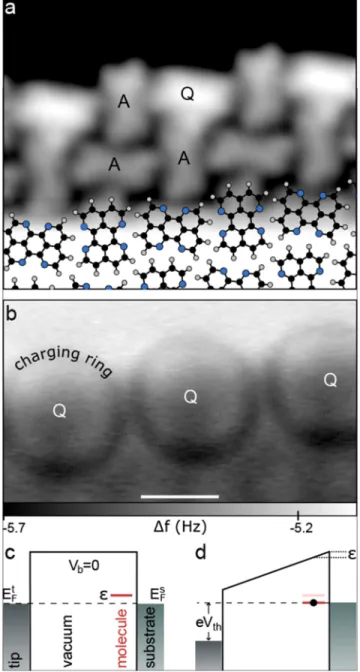
69molecules at the edges of self-assembled islands grown on Ag(111) can be deliberately switched in their charge state with the electric field from a scanning-probe tip. The self- assembled islands formed at room temperature have a peri- odic structure, in which each molecule is rotated by roughly Θ = 80
◦with respect to its four neighbors. Along the edges of the islands the molecules alternate in their orientation such that every other molecule exposes its α, α
0-diimine side to the out- side. These molecules, labeled as Q-type, exhibit a distinctly larger apparent height in STM images than all other molecules, labeled as A-type, as can be seen in Fig. 1(a). For negative bias voltages below a certain threshold value V
th, Q-type molecules change their appearance to being identical to A-type. For bias voltages close to the threshold value, rings were observed in the dI/dV and AFM images, which change their diame- ter with applied voltage (see Fig. 1(b)). From these and other characteristic observations being analogous to several previ- ous works,
70–75it could be concluded that the molecules are charged in the field of the scanning-probe junction. It was concluded further that without applied bias a localized state of the molecule was close enough to the substrate’s Fermi level, such that at a given threshold electric field the localized state can be shifted across the Fermi level of the substrate, which will change the (average) occupation of the state and hence the charge state. Hence, the observations suggest that Q-type molecules are neutral at zero bias voltage and become negatively charged at large negative bias voltages, whereas A-type molecules are permanently negatively charged. As we cannot assign the absolute charge state but only detect the tran- sitions, Q-type molecules might be already singly charged at zero bias voltage and become doubly charged at large negative bias voltages. In this case, all A-type molecules would have to be permanently doubly charged. We therefore regard this latter scenario as less likely.
FIG. 1. (a) Constant-current STM image of an island edge recorded at I = 9 pA,V = 0.2 V with a CO tip. At the bottom, the structure model of the molecular island is overlaid. (b) The frequency shift signal of the same area as in (a) recorded at constant-height (oscillation amplitudeA=0.95 Å, V =−1 V,∆z=1.3 Å, where∆z=0 refers to the vertical position above the center of the molecule in the interior of the island with the STM set-point parameters:I=9 pA,V=−1 V). Ring-like contours, observed only above Q molecules, are due to charging of these. For lower (more negative) sam- ple bias voltages, their diameter increases. Note that the image was acquired at quite large tip-sample distances, such that no intramolecular features are observable. ((c) and (d)) Schematic energy diagrams of the model explain- ing the charging: at zero sample bias voltage (c), one of the molecular levels is slightly above the Fermi energy of the substrate, namely, at an energy, such that at a threshold value for the sample biasVth(d), the level is shifted downward byin energy such that it crosses the Fermi level of the substrate resulting in a charging of the molecule. ((a) and (b)) Scale bar 1 nm.
It was further reported that close to the threshold volt-
age V
thfor a charge state transition, periodic switching of
the charge is directly driven by the cantilever motion in FM-
AFM. This coupling leads to appreciable signatures in the
measured frequency shift.
76In this regime, the integrated fre-
quency shift yields the tip-sample force that is due to a single
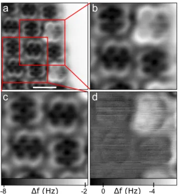
FIG. 2. (a) Constant-height AFM image of a molecular island edge. Imaging parameters:A=0.5 Å,V=0 V,∆z=−1.75 Å.∆z=0 refers to the vertical position above the Ag(111) surface with the tunneling set point parameters of I =1.2 pA,V =0.1 V. Scale bar 1 nm. ((b) and (c)) Zoom-ins of different areas from the image in (a) as indicated. (d) The difference image obtained by subtracting image (b) from image (c) allows the effects of one additional charge to be visualized. The relative position of the two subtracted images was adjusted such that contributions above A-type molecules were close to zero. The images in (a), (b), and (c) have the same∆f grayscale.
additional electron. Further, the signature of the dynamic charging response provides information on the electronic coupling of the molecule to the substrate.
Surprisingly, a localized state very close to the substrate’s Fermi level that was expected to be present could not be detected directly in differential conductance spectroscopy.
Instead, such spectroscopy shows steps located symmetrically around zero bias indicating inelastic excitations, which is not yet understood and beyond the scope of the present work.
IV. CONTRAST CHANGE UPON CHARGING A. Experimental findings
Fig. 2(a) shows an FM-AFM image of molecules at an edge of a self-assembled island at zero bias voltage. At zero voltage, A- and Q-type molecules are in different charge states.
Not only do they appear differently in STM images but also is their difference clearly visible in AFM images. Both types of molecules show a very similar contrast, it simply seems as if the Q-type molecules appear brighter, that is, with less negative frequency shift. In a previous STM work, different types of adsorbed phthalocyanine molecules were shown to exhibit charge bistability.
77In that case, the charge states were both stable within few tenths of a volt of applied bias voltages around zero, allowing to image the very same molecule in both charge states and to extract contrast changes. In the present case, this is not possible since the charge state switching shows no hysteretic behavior, and hence, for a given molecule at a given voltage there is only one charge state observed. How- ever, the highly regular arrangement in the self-assembled monolayer island still enables the extraction of a difference image as follows. As discussed previously, only every other molecule in the rim of the island is Q-type, while all oth- ers are A-type. Other than that, all molecules are placed in a highly regular way, thanks to self-assembly. This allows us to generate two cutouts of the larger image, each showing four molecules, but only one of them containing a Q-type molecule, see Figs. 2(b) and 2(c). These can be overlaid, with the iden- tical three molecules acting as alignment markers, and then subtracted from each other. The result, henceforth referred to as difference image, is displayed in Fig. 2(d). It shows a rel- atively homogeneous contrast over the molecule that differs in its charge state (top right in Fig. 2(d)) and no pronounced intra-molecular features.
B. Discussion
In AFM, several different forces may contribute to the signal. In the current context, electrostatic, van-der-Waals, and Pauli repulsion forces will be the relevant ones. Whereas the former two are quite long-range in nature and will therefore contribute also at larger distances, the fact that we do observe
FIG. 3. (a) Frequency shift∆f(z) versus distance curves at different sample bias voltages as indicated. For more negative sample bias voltages, the position of the charging feature shifts to larger distances∆z.∆z=0 refers to the vertical position above the Ag(111) surface with the STM set-point parameters of I=1.2 pA,V=0.1 V. Oscillation amplitudeA=0.3 Å. (b)∆f∗(z) response to the charging process obtained by subtracting a polynomial fit to the background signal (shown in red in (a) for three different spectra) from each measured curve in (a). The spectra are vertically offset by0.5 Hz for clarity. (c) The additional force resulting from the additional elementary charge as a function of the charging dip minima. The positions were extracted numerically by fitting each dip with a Gaussian function.
092327-4 Koci´cet al. J. Chem. Phys.146, 092327 (2017)
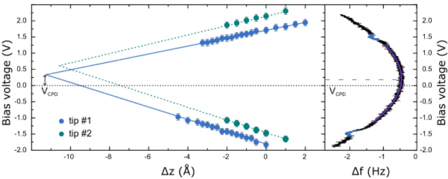
FIG. 4. Extracted threshold voltagesVthfor charging (left) as a function of tip height∆zat positive and negative bias voltages. The values were extracted from the observed dips in frequency shift spectra recorded for different∆zabove the center of the Q-type molecule. Such a∆f(V) spectrum is exemplary shown to the right for∆z=−1.75 Å. From the latter, one can also extract the CPD by fitting a Kelvin parabola, which in this particular case results in a value of 0.22 eV for the CPD (dashed horizontal line).∆z=0 corresponds to a STM set-point parameter above the Ag surface ofV=0.6 V,I=1.4 pA for tip #1, andV=0.6 V,I=1.9 pA for tip #2, respectively.
intra-molecular contrast in Fig. 2(a) indicates that Pauli repul- sion is relevant at the given tip-sample distances. Upon charg- ing, it can be expected that all three of the above-mentioned forces will change as a result of the extra electron interact- ing with the AFM tip. We expect that the relative change to the electrostatic force will be quite large as the net charge of the molecule changes dramatically. In contrast, the rela- tive change to the other two force components is expected to be rather weak, as for the latter all electrons of the molecule will contribute and the change associated with a single extra electron will hence be minor.
But not only can the extra electron directly affect the tip- molecule interaction, it may also result in slight relaxations within the molecule and of the molecule with respect to the substrate. For example, a charged molecule may interact more strongly with the substrate, such that a reduced adsorption height can be expected. Such relaxations would also contribute to the AFM signal indirectly. In this case, we would expect mostly the Pauli repulsion to be affected, as this is particularly short ranged, and hence, small geometric changes will have a large impact on Pauli repulsion. At first glance, one might assume that an overall vertical shift of the entire molecule would give rise to a homogeneous contrast change over the entire molecule. This, however, would not be the case. It was shown that the intramolecular resolution is due to Pauli repul- sion.
36,37Consequently, even a small vertical displacement of the entire molecule would greatly intensify the intramolecular contrast instead of adding to the homogeneous background.
Hence, if any molecular relaxations dominate the contrast, we would predominantly expect a difference image that shows strong features of the molecular geometric structure. As the contrast in Fig. 2(d) is relatively homogeneous we conclude that such contribution is apparently small. There is a small contribution of sub-molecular contrast; however, also over the A-type molecules a weak sub-molecular contrast can be observed, probably resulting from the non-prefect overlaps of the subtracted frames at different lateral positions. Different bending of the CO molecule at the functionalized tip may also contribute to the remaining sub-molecular contrast differences.
We tentatively assign the contrast change shown in Fig. 2(d) as being dominated by the electrostatic interaction between the extra electron and the tip. Interestingly, this con- trast while being homogeneous over the entire molecule under
consideration drops quite abruptly where the molecule ends.
This seems to indicate that the extra electron is delocalized over the entire molecule, giving rise to an AFM signal over the molecule but not next to it. Finally, the contrast change shows a linear gradient from inside to outside the molecular island. This may be due to a contribution that is not completely uniform and may be explained by the two α, α
0-diimine groups facing a different environment—one is adjacent to the hydro- gens of a neighboring molecule, the other is exposed to the bare silver terrace.
V. FORCE CHANGES UPON CHARGING A. Experimental findings
As is discussed in Ref. 66, it is possible to extract the change in force associated with the charging process as fol- lows. In frequency change ∆ f versus distance z spectra, the charging is observed as a distinct dip on the overall background signal that is typical of ∆ f (z) spectra in the attractive regime, as is shown in Fig. 3(a). The overall background signal can be fitted in the whole range except the feature by a polynomial of eighth order, such that the fit function and hence the back- ground signal can be subtracted. The resulting curve, shown in Fig. 3(b), is just a flat line with noise plus the character- istic dip due to the charging event. Integration over the dip in ∆ f (z) after background subtraction yields the force change associated with charging as
∆ F
charging= − 2k
0f
0dip
(∆ f (z) − ∆ f
◦(z))dz,
where f
◦( z ) is the fitted background signal of ∆ f ( z ), k
0the
stiffness of the cantilever, and f
0its unperturbed resonance fre-
quency. Although this force difference is only a few piconew-
tons, the charging can be readily detected. Whereas this force
was already mentioned in Ref. 66, here we show that how this
force evolves with tip-sample distance z. This is done by tak-
ing a series of ∆ f (z) spectra at different voltages (Fig. 3(a)), in
which the charging will occur at different tip-sample distances
because of the different voltages applied. Following the eval-
uation described above for each of the curves yields the force
differences ∆F
chargingas a function of distance. As in scanning
probe experiments, the absolute tip-sample distance is usu-
ally unknown, it is plotted against distance changes ∆z with
respect to a given set-point. The resulting data are shown in Fig. 3(c).
B. Discussion
When considering the results, it is important to note that each data point in Fig. 3(c) inevitably corresponds to a different applied voltage. The physical picture behind the charge state switching suggests that the charging always occurs at a certain threshold electric field that establishes the relation between threshold voltage V
thand distance (see also further below).
This implies that all data points in Fig. 3(c) correspond to the same electric field in the junction. A considerable fraction of the electrostatic interaction of the tip with a charge in the junction (fixed to the sample side) will arise simply from the force of the extra charge in the electric field that is due to the presence of the tip.
78,79If we assume the field to be the same for all data points, this contribution shall be constant with distance z.
Additional contributions may arise, for example, from the interaction of the charge with its image charge in the tip (that is, the tip’s screening). This force contribution will not depend on the applied bias voltage and fall off with increasing distance.
The trend in Fig. 3(c) seems to support the above pic- ture. Although the error bars are too large to extract any detailed dependencies, there is a contribution that decreases with increasing distance, but there seems to be also a constant distribution of about 1.5 pN, to which the signal asymptotically levels off. In this picture, the latter will be the interaction of the extra electron with the electric field of the tip. In conjunction to a future, more detailed theoretical analysis, this may pro- vide valuable insight into the forces acting in AFM junctions resulting from uncompensated charges.
VI. THRESHOLD VOLTAGE FOR CHARGING A. Experimental findings
As already discussed, the threshold voltage for charg- ing V
thdepends on the tip-sample distance. Whereas in Ref.
66 only at negative bias voltage a single charging event was reported, one can observe also a similar charging phenomenon at large positive bias voltages. Fig. 4 (right panel) shows a typ- ical ∆ f (V ) spectrum, recorded at a fixed tip-sample distance z. Whereas the overall parabolic shape of the curve is gov- erned by electrostatics,
44,52,57two dips, one each at positive and negative bias, indicate a charging event. Similar ∆ f (V) spectra were recorded at a set of different distances z, and the dip positions were extracted as a function of tip displacement
∆z. In Fig. 4 (left panel), the bias voltages, at which charging was observed, are plotted against ∆z for two different tip apices in blue and green, respectively. Each data set for one particular charging event and one of the tips can be well fitted by a line.
Each two lines, corresponding to different charging processes but the same tip apex, cross at ∆z ≈ − 11 Å and small positive bias voltage.
B. Discussion
The model for charging as discussed in Refs. 29, 65–67, 70, 74, and 80 suggests that the electric field in the junction
shifts an electronic level of the molecule across the Fermi level, such that its occupation changes. In light of this, it is not obvi- ous, why two charging events can be observed. Maybe the two charging events correspond to the very same molecular orbital, but two different charging possibilities, separated by the Coulomb charging energy U. Hence, in this scenario, an elec- tron would be either added or removed from the same orbital at negative and positive bias voltages, respectively. The Coulomb charging energy U for a molecule directly adsorbed on a metal surface is greatly reduced due to screening and therefore may well be of the required magnitude. However, this would require the Q-type molecules to be already singly charged at zero bias and to become doubly charged at large negative bias voltages.
We refrain from making such an assignment. We just note that two or more charging levels have been observed for molecules before.
65,67Irrespective of the nature of the two levels that are being shifted across the Fermi level, we can investigate whether the observed distance dependence fits to a simple model accord- ing to the picture behind the charging. As the fraction of the total bias voltage that drops between molecule and sub- strate is relatively small, the electronic level responsible for charging has to be close to the Fermi level also without any field in the junction. May this level for zero field be at an energy with respect to the Fermi level of the surface. As one observes two charging events for opposite polarity, we have to assume two levels being close to the Fermi level at energies
1and
2. In a simple plate capacitor model, the frac- tion of the total bias voltage that drops between molecule and substrate is simply given by the ratio of molecule-substrate distance d
msdivided by the total tip-substrate distance d
ts. Although at the atomic scale for adsorption of a molecule directly on the metal substrate the molecule-substrate distance d
msis not a very well defined quantity, one may view this as an effective molecule-substrate distance d
msthat accounts for the possibility of an electric field to shift the molecular levels.
One has to keep in mind that for a non-zero contact poten- tial difference (CPD) between tip and sample, even at zero bias voltage there is a finite electric field across the junction (see Fig. 5(a)). Only at compensated CPD, that is, at V = V
CPDthe electric field vanishes. Although this is very well known from Kelvin probe force spectroscopy, it is usually less obvious in pure STM experiments. Hence, the shift of the molecular levels equals ∆E = e(V − V
CPD)d
ms/d
ts, where e denotes the elementary charge. In the case of a charging event, this energy shift equals to −
1,2such that the levels are aligned with the Fermi level of the substrate. Solving the above equation with respect to the bias voltage V , which then becomes the threshold voltage V
th, we obtain
V
th= V
CPD−
1,2d
tse d
ms. (1)
Interestingly, this provides indeed a linear dependence of the threshold voltage with the tip-substrate distance d
ts, which in a more depictive description can be understood as follows.
The charging condition is associated with a certain electric
field in the junction. In the simple plate capacitor model, the
potential drop has to increase linearly with distance to keep the
092327-6 Koci´cet al. J. Chem. Phys.146, 092327 (2017)
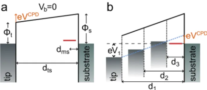
FIG. 5. (a) Illustration of the potential drop in the junction without bias volt- age resulting from a finite contact potential difference (CPD), which results from a difference of the work function of the tipΦtand sampleΦs. (b) Illus- tration of the linear relationship of threshold voltage and distance as a result of the constant electric field required for charging the molecule. For different tip-substrate distances, here exemplified asd1,2,3, the quantity (V−VCPD) has to be proportional to the distance (see dashed blue line) to keep a constant field that is required for charging the molecule.
electric field and thereby ∆E constant, giving rise to the linear scaling of V
thwith tip-substrate spacing d
ts(see Fig. 5(b)). This fits very well to the observed behavior. Moreover, the above equation suggests an interesting implication for the crossing point of the line fits in Fig. 4: irrespective of the particular values of
1,2, all lines will cross at d
ts= 0 and V
CPD. Hence, the determination of the crossing points from observations as displayed in Fig. 4 should yield valuable information, namely, the local contact potential difference and the absolute tip-to- substrate distance by providing d
ts= 0 at the crossing point of the line fits. Note that the latter quantity is usually unknown in scanning probe experiments, such that having another way to estimate this quantity may be useful. The data in Fig. 4 suggest that the tip-to-substrate distance d
tsis ≈ 11 Å for the set-point parameters of 1.4 pA and 1.9 pA at 0.6 V, respectively. The local contact potential difference for the two tip apices has positive values of ≈ 0.3 and ≈ 0.7 eV, respectively. This value can be directly compared to the one measured with Kelvin probe spectroscopy. For one of the two tip apices, the Kelvin parabola is plotted in Fig. 4. The extracted value of CPD of 0.22 eV fits very well to the above value of ≈ 0.3 eV for this particular tip.
As the crossing point of the two line fits is quite far from the range, in which data points are available, the question of the confidence range of the fit arises. To this end, we extracted the error margins for each of the two line fits exemplary for the dataset, for which more data points were available. From this, we calculated the error margins of the crossing point, cor- responding to a standard deviation of 0.06 eV of the extracted CPD value and 0.3 Å for the tip-substrate separation.
Another more fundamental question arises with respect to the validity of the plate capacitor model. The plate capacitor model can be justified by the tip radius being typically at least an order of magnitude larger than the tip-sample spacing. In the following, we would like to discuss that in some more detail.
First, one has to consider, where in the junction the potential matters for the shift of the energetic position of the particular state that is to be shifted across the Fermi level. According to first order perturbation theory (for non-degenerate states), this shift is given by ∆E = hΨ
0|∆V (~ r) |Ψ
0i , where Ψ
0is the unper- turbed state that is being shifted in energy and ∆V is the change in potential resulting from the presence of the tip. This indi-
cates that the potential drop only at the position of the molecule matters; an almost trivial but still important piece of informa- tion. This observation clarifies, what V
CPDin Equation (1) exactly refers to, namely, this is the bias voltage, at which the potential at the position of the molecule’s state remains the same as without the tip being present. Kelvin probe spec- troscopy is known to be subject to spatial averaging.
46,81In other words, in Kelvin probe spectroscopy the CPD of different tip and sample regions matters. In contrast, the determination of the CPD from local charging events as reported here is apparently more local and hence less sensitive to spatial aver- aging. This might be particularly interesting, if the charging occurs at the tip instead of the sample side as was reported recently.
67Next we reconsider the scaling of ∆E with bias volt- age and distance. Irrespective of the shape of the junction and the detailed spatial dependence of the potential, it is rea- sonable to assume that the change in potential ∆V (~ r) scales linearly with V − V
CPD79in good approximation. As long as V
CPDitself does not depend on tip-substrate distance d
ts, we thus obtain that ∆E = αe(V −V
CPD) with a lever arm α that is an unknown function of d
ts. With this, the threshold voltage reads
V
th= V
CPD−
1,2e α(d
ts) . (2) As discussed above, in the simple plate capacitor model, the potential drop has to increase linearly with distance to keep the electric field and thereby ∆E constant and thereby match the charging condition. This gives rise to the linear scaling of V
thwith tip-substrate spacing d
ts. This simple relationship is definitely questionable for a three-dimensional junction devi- ating strongly from a plate capacitor. However, considering that only the potential at the position of the molecule matters and for tip-sample spacings of several Ångstr¨oms and tip cur- vatures of tens of nanometers, the plate capacitor model might be a good approximation. We note that also other effects may give rise to non-linear behaviour. For example, relaxations of the molecule arising from the bias voltage would give rise to such a nonlinear scaling.
Most importantly, irrespective of all these considerations, it is simply an experimental observation that the data shown in Fig. 4 do exhibit a linear z dependence. So even if the lin- ear behavior would break down for shorter distances, one may still consider whether the crossing point of the line fits provides valuable information. Equation (2) reveals that irrespective of the functional dependence of α( d
ts) the threshold voltages for different charging events will cross at V
th= V
CPD, so the extraction of the contact potential difference from this anal- ysis seems independent from the dimensionality of the model.
In addition, we argue that—as long as the experimental data
do show a linear behavior—d
tsextracted from fitting the data
provides the effective distance over which the junction poten-
tial drops. For metallic tips, we expect that this will correspond
closely to the geometrical distance, whereas for functionalized
tips there will be deviations. Future numerical simulations of
the potential drop in the junction, for example, by means of
density functional theory, could establish such a relationship
more firmly.
VII. CONCLUSION
Here, we discussed three aspects of the charging of molecules in the junction of a FM-AFM. We visualized the dif- ference in AFM images upon charging of the molecules from a suitable subtraction of images. The contrast reveals that the extra electron is delocalized over the entire molecule and sug- gests that the main contribution to the difference image stems from electrostatic interaction. The changes of force associated with the charging were quantified as a function of distance and were found to only weakly decay with increasing dis- tance. Finally, we investigated the distance dependence of the threshold voltage required for charging. The analysis based on a very simple model suggests that these dependencies allow an estimation of the local contact potential difference as well as the tip-sample spacing.
ACKNOWLEDGMENTS
This work is dedicated to the memory of Thomas Wandlowski.
Financial support from the Marie Curie Initial Training Network “MOLESCO” (No. 606728) is gratefully acknowl- edged.
1M. C. Petty, M. R. Bryce, and D. Bloor,An Introduction to Molecular Electronics(Oxford University Press, USA, 1995).
2A. Aviram and E. D. Ratner,Molecular Electronics: Science and Technology (The New York Academy of Sciences, 1998).
3M. A. Reed and T. Lee,Molecular Nanoelectronics(American Scientific Publishers, Stevenson Ranch, CA, 2003).
4J. R. Reimers,Molecular Electronics III(New York Academy of Sciences, 2003), Vol. 1006.
5Y. Selzer and D. L. Allara,Annu. Rev. Phys. Chem.57, 593 (2006).
6C. Joachim and M. A. Ratner,Proc. Natl. Acad. Sci. U. S. A.102, 8801 (2005).
7G. Cuniberti, G. Fagas, and K. Richter,Introducing Molecular Electronics (Springer, 2006).
8J. C. Cuevas and E. Scheer,Molecular Electronics: An Introduction to Theory and Experiment(World Scientific, 2010), Vol. 1.
9K. Slowinski, R. V. Chamberlain, C. J. Miller, and M. Majda,J. Am. Chem.
Soc.119, 11910 (1997).
10H. Ohnishi, Y. Kondo, and K. Takayanagi,Nature395, 780 (1998).
11X. D. Cui, A. Primak, X. Zarate, J. Tomfohr, O. F. Sankey, A. L. Moore, T. A. Moore, D. Gust, G. Harris, and S. M. Lindsay,Science294, 571 (2001).
12J. Reichert, R. Ochs, D. Beckmann, H. B. Weber, M. Mayor, and H. v. L¨ohneysen,Phys. Rev. Lett.88, 176804 (2002).
13B. Xu and N. J. Tao,Science301, 1221 (2003).
14L. Venkataraman, J. E. Klare, I. W. Tam, C. Nuckolls, M. S. Hybertsen, and M. L. Steigerwald,Nano Lett.6, 458 (2006).
15F. Chen, J. Hihath, Z. Huang, X. Li, and N. J. Tao,Annu. Rev. Phys. Chem.
58, 535 (2007).
16J. Park, A. N. Pasupathy, J. I. Goldsmith, C. Chang, Y. Yaish, J. R. Petta, M. Rinkoski, J. P. Sethna, H. D. Abru˜na, P. L. McEuen, and D. C. Ralp, Nature417, 722 (2002).
17S. Kubatkin, A. Danilov, M. Hjort, J. Cornil, J.-L. Bredas, N. Stuhr-Hansen, P. Hedeg˚ard, and T. Bjørnholm,Nature425, 698 (2003).
18X. Xiao, B. Xu, and N. Tao,J. Am. Chem. Soc.126, 5370 (2004).
19X. Xiao, B. Xu, and N. J. Tao,Nano Lett.4, 267 (2004).
20A. R. Champagne, A. N. Pasupathy, and D. C. Ralph,Nano Lett.5, 305 (2005).
21C. Joachim, J. K. Gimzewski, R. R. Schlittler, and C. Chavy,Phys. Rev.
Lett.74, 2102 (1995).
22L. A. Bumm, J. J. Arnold, M. T. Cygan, T. D. Dunbar, T. P. Burgin, L. Jones II, D. L. Allara, J. M. Tour, and P. S. Weiss,Science271, 1705 (1996).
23Z. J. Donhauser, B. A. Mantooth, K. F. Kelly, L. A. Bumm, J. D. Monnell, J. J. Stapleton, D. W. Price, A. M. Rawlett, D. L. Allara, J. M. Tour, and P. S. Weiss,Science292, 2303 (2001).
24J. Kr¨oger, N. N´eel, and L. Limot,J. Phys.: Condens. Matter20, 223001 (2008).
25R. Berndt, J. Kr¨oger, N. N´eel, and G. Schull,Phys. Chem. Chem. Phys.12, 1022 (2010).
26S. Schmaus, A. Bagrets, Y. Nahas, T. K. Yamada, A. Bork, M. Bowen, E. Beaurepaire, F. Evers, and W. Wulfhekel,Nat. Nanotechnol.6, 185 (2011).
27M. Koch, F. Ample, C. Joachim, and L. Grill,Nat. Nanotechnol.7, 713 (2012).
28J. Repp, G. Meyer, F. E. Olsson, and M. Persson,Science305, 493 (2004).
29S. W. Wu, G. V. Nazin, X. Chen, X. H. Qiu, and W. Ho,Phys. Rev. Lett.93, 236802 (2004).
30J. Repp, G. Meyer, S. M. Stojkovi´c, A. Gourdon, and C. Joachim,Phys.
Rev. Lett.94, 026803 (2005).
31F. E. Olsson, S. Paavilainen, M. Persson, J. Repp, and G. Meyer,Phys. Rev.
Lett.98, 176803 (2007).
32K. J. Franke, G. Schulze, N. Henningsen, I. Fern´andez-Torrente, J. I. Pascual, S. Zarwell, K. R¨uck-Braun, M. Cobian, and N. Lorente,Phys. Rev. Lett.100, 036807 (2008).
33W. Guo, S. X. Du, Y. Y. Zhang, W. A. Hofer, C. Seidel, L. F. Chi, H. Fuchs, and H.-J. Gao,Surf. Sci.603, 2815 (2009).
34N. Pavliˇcek, I. Swart, J. Niedenf¨uhr, G. Meyer, and J. Repp,Phys. Rev. Lett.
110, 136101 (2013).
35B. Warner, F. El Hallak, H. Pr¨user, J. Sharp, M. Persson, A. J. Fisher, and C. F. Hirjibehedin,Nat. Nanotechnol.10, 259 (2015).
36L. Gross, F. Mohn, N. Moll, P. Liljeroth, and G. Meyer,Science325, 1110 (2009).
37L. Gross, F. Mohn, N. Moll, B. Schuler, A. Criado, E. Guiti´an, D. Pe˜na, A. Gourdon, and G. Meyer,Science337, 1326 (2012).
38F. Mohn, J. Repp, L. Gross, G. Meyer, M. S. Dyer, and M. Persson,Phys.
Rev. Lett.105, 266102 (2010).
39T. Leoni, O. Guillermet, H. Walch, V. Langlais, A. Scheuermann, J. Bonvoisin, and S. Gauthier,Phys. Rev. Lett.106, 216103 (2011).
40N. Pavliˇcek, B. Fleury, M. Neu, J. Niedenf¨uhr, C. Herranz-Lancho, M. Ruben, and J. Repp,Phys. Rev. Lett.108, 086101 (2012).
41M. Nonnenmacher, M. P. O’Boyle, and H. K. Wickramasinghe,Appl. Phys.
Lett.58, 2921 (1991).
42S. Kitamura and M. Iwatsuki,Appl. Phys. Lett.72, 3154 (1998).
43H. Jacobs, P. Leuchtmann, O. J. Homan, and A. Stemmer,J. Appl. Phys.
84, 1168 (1998).
44T. K¨onig, G. H. Simon, H.-P. Rust, G. Pacchioni, M. Heyde, and H.-J.
Freund,J. Am. Chem. Soc.131, 17544 (2009).
45S. A. Burke, J. M. LeDue, Y. Miyahara, J. M. Topple, S. Fostner, and P. Gr¨utter,Nanotechnology20, 264012 (2009).
46F. Krok, K. Sajewicz, J. Konior, M. Goryl, P. Piatkowski, and M. Szymonski, Phys. Rev. B77, 235427 (2008).
47S. Kawai, A. Sadeghi, X. Feng, P. Lifen, R. Pawlak, T. Glatzel, A. Willand, A. Orita, J. Otera, S. Goedecker, and E. Meyer,ACS Nano7, 9098 (2013).
48Y. Miyahara, J. Topple, Z. Schumacher, and P. Gr¨utter,Phys. Rev. Appl.4, 054011 (2015).
49F. Mohn, L. Gross, N. Moll, and G. Meyer,Nat. Nanotechnol.7, 227 (2012).
50B. Schuler, S.-X. Liu, Y. Geng, S. Decurtins, G. Meyer, and L. Gross,Nano Lett.14, 3342 (2014).
51F. Albrecht, J. Repp, M. Fleischmann, M. Scheer, M. Ondr´aˇcek, and P. Jel´ınek,Phys. Rev. Lett.115, 076101 (2015).
52L. Gross, F. Mohn, P. Liljeroth, J. Repp, F. J. Giessibl, and G. Meyer,Science 324, 1428 (2009).
53W. Steurer, S. Fatayer, L. Gross, and G. Meyer,Nat. Commun.6, 8353 (2015).
54P. Rahe, R. P. Steele, and C. C. Williams,Nano Lett.16, 911 (2016).
55M. T. Woodside and P. L. McEuen,Science296, 1098 (2002).
56G. A. Steele, A. K. H¨uttel, B. Witkamp, M. Poot, H. B. Meerwaldt, L. P. Kouwenhoven, and H. S. J. van der Zant,Science325, 1103 (2009).
57R. Stomp, Y. Miyahara, S. Schaer, Q. Sun, H. Guo, P. Gr¨utter, S. Studenikin, P. Poole, and A. Sachrajda,Phys. Rev. Lett.94, 056802 (2005).
58J. Zhu, M. Brink, and P. L. McEuen,Appl. Phys. Lett.87, 242102 (2005).
59Y. Azuma, M. Kanehara, T. Teranishi, and Y. Majima,Phys. Rev. Lett.96, 016108 (2006).
60S. D. Bennett, L. Cockins, Y. Miyahara, P. Gr¨utter, and A. A. Clerk,Phys.
Rev. Lett.104, 017203 (2010).
61L. Cockins, Y. Miyahara, S. D. Bennett, A. A. Clerk, S. Studenikin, P. Poole, A. Sachrajda, and P. Gr¨utter,Proc. Natl. Acad. Sci. U. S. A.107, 9496 (2010).
62A. Tekiel, Y. Miyahara, J. M. Topple, and P. Gr¨utter,ACS Nano7, 4683 (2013).
63L. Cockins, Y. Miyahara, S. D. Bennett, A. A. Clerk, and P. Gr¨utter,Nano Lett.12, 709 (2012).
092327-8 Koci´cet al. J. Chem. Phys.146, 092327 (2017)
64A. Roy-Gobeil, Y. Miyahara, and P. Gr¨utter,Nano Lett.15, 2324 (2015).
65C. Lotze, Ph.D. thesis, Freie Universit¨at Berlin, Berlin, Germany, 2013.
66N. Koci´c, P. Weiderer, S. Keller, S. Decurtins, S.-X. Liu, and J. Repp,Nano Lett.15, 4406 (2015).
67C. Wagner, M. F. B. Green, P. Leinen, T. Deilmann, P. Kr¨uger, M. Rohlfing, R. Temirov, and F. S. Tautz,Phys. Rev. Lett.115, 026101 (2015).
68F. J. Giessibl,Appl. Phys. Lett.76, 1470 (2000).
69T. Brietzke, W. Mickler, A. Kelling, and H.-J. Holdt,Dalton Trans.41, 2788 (2012).
70N. A. Pradhan, N. Liu, C. Silien, and W. Ho,Phys. Rev. Lett.94, 076801 (2005).
71G. V. Nazin, X. H. Qiu, and W. Ho,Phys. Rev. Lett.95, 166103 (2005).
72K. Teichmann, M. Wenderoth, S. Loth, R. G. Ulbrich, J. K. Garleff, A. P. Wijnheijmer, and P. M. Koenraad,Phys. Rev. Lett. 101, 076103 (2008).
73V. W. Brar, R. Decker, H.-M. Solowan, Y. Wang, L. Maserati, K. T. Chan, H. Lee, C¸ . O. Girit, A. Zettl, S. G. Louie, M. L. Cohen, and M. F. Crommie, Nat. Phys.7, 43 (2011).
74I. Fern´andez-Torrente, D. Kreikemeyer-Lorenzo, A. Str´o˙zecka, K. J. Franke, and J. I. Pascual,Phys. Rev. Lett.108, 036801 (2012).
75P. Sessi, T. Bathon, K. A. Kokh, O. E. Tereshchenko, and M. Bode,Adv.
Mater.28, 10073 (2016).
76M. Ondr´aˇcek, P. Hapala, and P. Jel´ınek,Nanotechnology27, 274005 (2016).
77I. Swart, T. Sonnleitner, and J. Repp,Nano Lett.11, 1580 (2011).
78L. Gross, B. Schuler, F. Mohn, N. Moll, N. Pavliˇcek, W. Steurer, I. Scivetti, K. Kotsis, M. Persson, and G. Meyer,Phys. Rev. B90, 155455 (2014).
79J. L. Neff and P. Rahe,Phys. Rev. B91, 085424 (2015).
80L. Liu, T. Dienel, R. Widmer, and O. Gr¨oning,ACS Nano9, 10125 (2015).
81S. Sadewasser and T. Glatzel,Kelvin Probe Force Microscopy(Springer, 2012).