EuO and Eu on metal crystals and graphene: interface effects and
epitaxial films
I n a u g u r a l - D i s s e r t a t i o n zur
Erlangung des Doktorgrades
der Mathematisch-Naturwissenschaftlichen Fakult¨ at der Universit¨ at zu K¨ oln
vorgelegt von
Dipl.-Phys. Daniel F. F¨orster
aus Stolberg (Rheinland)
K¨ oln 2011
Berichterstatter: Prof. Dr. Thomas Michely (Gutachter) Prof. Dr. L. Hao Tjeng Vorsitzender
der Pr¨ ufungskommission: Prof. Dr. Achim Rosch
Tag der m¨ undlichen Pr¨ ufung: 14.10.2011
Abstract
Growth of the ferromagnetic semiconductor EuO was studied on the metal crystals Ni(100) and Ir(111) and on graphene. Primarily, characterisation was done by means of in-situ scanning tunnelling microscopy (STM) and low energy electron diffraction.
The epitaxy on the metal crystals is strongly influenced by interface effects which lead to a complicated growth behaviour in the sub-monolayer regime, especially on Ni(100).
Therefore, also films of sub-monolayer thickness were analysed in detail for these sub- strates.
Eu oxide on Ni(100) shows a variety of different surface phases in the sub-monolayer regime, depending on the growth temperature and the ratio of the Eu and O fluxes.
Hence, a careful selection of the initial growth parameters is decisive to obtain a surface oxide suitable for subsequent epitaxy of single phase EuO(100). After creation of a 3 layer thick coalesced oxide film, for subsequent growth a distillation technique can be applied. Ex-situ X-ray adsorption spectroscopy and magneto-optical Kerr effect microscopy measurements of thicker films on Ni(100) are consistent with stoichiometric single phase EuO with bulk properties.
On Ir(111) initially only islands of polar EuO(111) grow, but formation of EuO(100) sets in before the first oxide layer is completed. The ratio of EuO(100) to EuO(111) is thereby influenced by the ratio of the Eu and O fluxes. Thus, the EuO films on Ir(111) consist of a phase mixture of EuO(111) and three rotational domains of EuO(100).
The thinnest structure of the EuO(111) is a bilayer. Field emission resonances revealed a work function increase of 6 eV for this structure compared to EuO(100). Despite the polarity, the bilayer shows no obvious reconstruction which could reduce the high electric field. Triangular reconstruction motifs were found for the third EuO(111) layer.
On graphene EuO can be grown as thin film of distinct, {100}-faceted grains which are oriented to the substrate at a sufficiently high growth temperature. As the EuO on graphene is not affected by interface effects, the initial growth stage is not crucial.
Thus, the growth of these grains is far less sensitive to the ratio of Eu and O fluxes than the EuO growth on Ni(100).
Appropriate annealing of EuO(100) films generates sufficient conductivity for STM and
electron spectroscopies, even for films of 100 nm thickness. Oxygen vacancies were
directly imaged by STM. They are of decisive importance for the metal-to-insulator transition of EuO around the temperature of the ferromagnetic-to-paramagnetic tran- sition. Tunnelling spectra of EuO were recorded for the first time. For EuO(100) with 1% O vacancies in the topmost layer they exhibit states about 500 meV above the Fermi level which are most probably related to O vacancies.
On all substrates, monolayer high EuO(100) films have a contracted lattice which ex- pands with increasing film thickness. Even if the substrate applies compressive biaxial stress, the EuO bulk lattice constant is almost reached for 5 nm film thickness. This leaves little hope for an increase of the Curie temperature through epitaxial compression.
During the investigation of the EuO on graphene, intercalation of Eu between the graphene and its Ir(111) substrate was observed and analysed further. For Eu depo- sition at 720 K a variety of equilibrium intercalate structures occur, dependent on the deposited Eu amount, all of which have a height of one monolayer. The dimensions and orientations of these structures are determined by binding energy differences within the unit cell of the graphene moir´ e on Ir(111). The energetically preferred lattice of the intercalated Eu is a p(2×2) structure, but intercalation continues until a denser ( √
3 × √
3)R30
◦structure is saturated. Angular resolved photoemission spectroscopy finds a shift of the graphene’s Dirac cone by −1.5 eV for both of these structures.
For closed graphene films, intercalation is hindered by a penetration barrier for temper- atures below 400 K. The adsorption and equilibrium surface phases of Eu on graphene were investigated in the temperature range from 35 K to 400 K and for coverages ranging from a small fraction of a saturated monolayer to the second layer. Using density func- tional theory, including the 4f-shell Coulomb interactions and modelling of the electronic interactions, excellent agreement with the experimental results for the equilibrium ad- sorbate phase, adsorbate diffusion, and work function was obtained. Most remarkable, at 300 K in an intermediate coverage range a phase of uniformly distributed Eu clusters coexists in two dimensional equilibrium with large Eu-islands in a ( √
3× √
3)R30
◦struc- ture. The formation of the cluster phase is driven by the interplay of three effects: First, the metallic Eu-Eu binding leads to the local stability of ( √
3 × √
3)R30
◦structures.
Second, electrons lower their kinetic energy by leaving the Eu clusters, thereby doping
graphene. Third, the Coulomb energy penalty associated with the charge transfer from
Eu to graphene is strongly reduced for smaller clusters.
Contents
Abstract i
Table of Contents iii
Frequently used symbols vii
1 Introduction 1
2 Background 3
2.1 EuO - a manifold material . . . . 3
2.1.1 Electronic structure . . . . 4
2.1.2 N-Doping . . . . 5
2.1.3 Surface State . . . . 6
2.1.4 Thin Films . . . . 7
2.2 Surface oxides . . . . 8
2.3 Polar oxide surfaces . . . . 9
2.4 Graphene . . . . 12
2.4.1 Electronic Properties . . . . 12
2.4.2 Graphene on Ir(111) . . . . 13
2.4.3 Adsorption . . . . 15
2.4.4 Intercalation . . . . 16
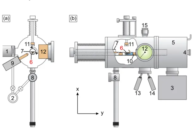
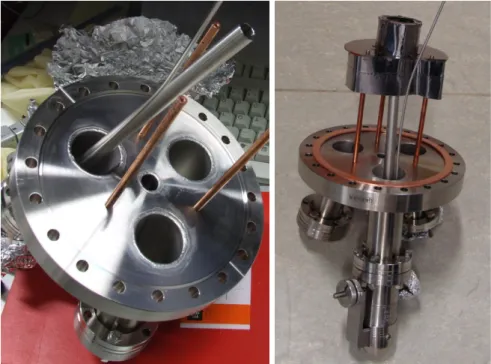
3 Experimental Setup 19 3.1 UHV system Athene . . . . 19
3.1.1 Sample Holder and Base Plate . . . . 20
3.1.2 MBE station . . . . 23
3.2 The hedgehog STM . . . . 25
3.2.1 Etching of Ir Tips . . . . 27
4 Experimental procedures 29 4.1 Sample preparation . . . . 29
4.1.1 Ni(100) . . . . 29
4.1.2 Ir(100) . . . . 29
4.1.3 Ir(111) . . . . 30
4.1.4 Graphene on Ir(111) . . . . 30
CONTENTS
4.2 Film growth . . . . 31
4.2.1 Gas Inlet Calibration . . . . 31
4.2.2 Evaporation . . . . 32
4.2.3 EuO growth . . . . 32
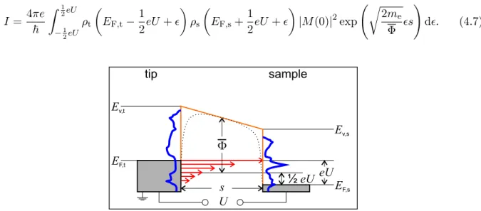
4.3 Scanning tunnelling microscopy and spectroscopy . . . . 33
4.3.1 The one dimensional tunnelling barrier . . . . 33
4.3.2 dI/dU measurements . . . . 35
4.3.3 Field Emission Resonances (FERs) . . . . 38
4.3.4 I(s) measurements . . . . 39
4.4 Low energy electron diffraction . . . . 40
5 EuO on Ni(100) 41 5.1 The surface oxides . . . . 41
5.1.1 EuO(111) . . . . 43
5.1.2 Stripe islands . . . . 47
5.1.3 Clusters . . . . 51
5.1.4 p(5×5) superstructure . . . . 55
5.2 2.5 Monolayers and beyond . . . . 58
5.2.1 Initial growth of EuO(100) films . . . . 59
5.2.2 Annealing in Eu vapour . . . . 64
5.2.3 100 nm thick EuO(100) films . . . . 65
5.2.4 Epitaxial strain . . . . 69
5.3 Summary . . . . 71
6 EuO on Iridium 73 6.1 EuO on Ir(111) . . . . 73
6.1.1 Film thickness dependence . . . . 74
6.1.2 Flux ratio dependence . . . . 79
6.1.3 Work function of the polar EuO(111) . . . . 82
6.1.4 Temperature dependence . . . . 84
6.2 EuO on Ir(100) . . . . 87
6.3 Summary . . . . 89
7 EuO on graphene on Ir(111) 91 7.1 Morphology of the EuO grains . . . . 91
7.2 Spectroscopy . . . . 96
7.3 Summary . . . . 99
CONTENTS
8 Eu on and intercalated under graphene on Ir(111) 101
8.1 Eu intercalate patterns oriented along the graphene moir´ e . . . . 102
8.1.1 Chemical stability of intercalated Eu . . . . 104
8.1.2 Intercalate structures . . . . 104
8.1.3 Intercalate patterns . . . . 108
8.1.4 Graphene doping . . . . 113
8.2 Eu on Graphene . . . . 117
8.2.1 Eu adsorption at 35 K . . . . 117
8.2.2 Room temperature Eu adsorption . . . . 120
8.2.3 Annealing . . . . 123
8.2.4 DFT Results . . . . 124
8.2.5 Discussion . . . . 128
8.3 Work function comparisons . . . . 134
8.4 Summary . . . . 137
9 Summary and outlook 139 9.1 Summary . . . . 139
9.2 Outlook . . . . 142
References 145 A Eu adsorption on Ir(111) 169 A.1 Eu adsorbate structures on Ir(111) . . . . 169
B Construction plans 173
C Publications 193
D Kurzzusammenfassung 195
Acknowledgements 197
Offizielle Erkl¨ arung 199
CONTENTS
Frequently used symbols and abbreviations
Θ exposure: amount of material hitting the surface with or without sticking
f
EuEuropium atom flux
f
OOxygen atom flux
I
tTunnelling current
T
CCritical Temperature; here mostly the ferromagnetic transition temperature
U
sSample bias voltage
ARPES Angle Resolved PhotoEmission Spectroscopy
DOS Density Of States
FWHM Full Width at Half Maximum LDOS Local Density Of States
LEED Low Energy Electron Diffraction MIT Metal to Insulator Transition STM Scanning Tunnelling Microscopy STS Scanning Tunnelling Spectroscopy
UHV Ultra High Vacuum
E
FFermi level
bcc base centred cubic
BL BiLayer
DFT density functional theory
fcc face centred cubic
hcp hexagonal close packed
ML MonoLayer
MLE MonoLayer Equivalents
MOKE Magneto Optical Kerr Effect
NN Nearest Neighbour
CVD Chemical Vapour Deposition
FER Field Emission Resonance
CONTENTS
L Langmuir = 10
−6Torr · s ≈ 1.33 × 10
−6mbar · s QMS Quadrupole Mass Spectrometer
SBZ Surface Brillouin Zone
TPG Temperature Programmed Growth
1 Introduction
Europium Monoxide (EuO) is a compound with several unique properties and was first grown in the 1950s [1]. Since 1961 it has aroused considerable interest, especially due to the discovery of the simultaneous presence of ferromagnetism and semiconductivity [2], which is a rare combination. At room temperature stoichiometric EuO is a paramagnetic semiconductor with a band gap of 1.1 eV [3] and becomes ferromagnetic below 69 K. Its high exchange splitting of the conduction band below T
Cresults in a high spin polarisation of the charge carriers at the Fermi edge [4; 5]. This, together with the semiconductivity makes EuO an attractive material for spin-injection into semiconductor- based spintronic devices. Hence spintronics was the main motivation for EuO research during the last decade [4–35]. This was boosted by the improvements of thin film deposition techniques, which lead to the possibility of epitaxially integrating EuO with mainstream semiconductors such as silicon and GaN [16].
Spintronics [36] is an abbreviation for spin-based electronics, which means either the addition of the spin degree of freedom to conventional charge-based electronic devices or the usage of the spin alone as carrier for the information. Potential advantages of spintronics compared to conventional semiconductor devices are non-volatility, increased data processing speed, decreased electric power consumption, and increased integration densities [37]. Achieving efficient coherent spin injection into a semiconductor is a key requirement for spintronics and needs a material which has highly spin polarised charge carriers at the Fermi edge and whose conductivity can be matched to the same order of magnitude as that of the semiconductor [36; 38]. EuO fulfils these criterions [16]
but has for applications the practical disadvantage of the low ferromagnetic transition temperature of 69 K. An increase of T
Ccan be achieved either by doping [8; 14; 39] or by compressive strain [17; 40; 41]. Increasing T
Cby doping has the disadvantage of influencing the conductivity and thus creates conflicts with the requirement of conductivity matching. This leaves the possibility of compressive strain, whereby due to the low Poisson ratio of EuO already biaxial strain increases T
C[17]. Biaxial compressive strain can be achieved by compressive epitaxial stress (i.e., by epitaxial growth of thin films on a substrate with slightly smaller surface lattice constant). By fulfilling the principal aim of this thesis, the epitaxial growth of EuO thin films on conductive substrates, it was also possible to analyse the possibility of introducing compressive biaxial strain by using substrates with smaller surface lattice constants, which are Ni(100) and graphene on Ir(111).
The second most remarkable peculiarity of EuO is the metal to insulator transition (MIT) which
occurs simultaneously with the ferromagnetic transition. The change in resistivity can exceed 10
orders of magnitude [42–44], which is the largest value ever observed during an MIT. Hence it
motivated several investigations [45–56], especially as the mechanism of the MIT is still not fully
understood. It only occurs for doped EuO and the reason is supposed to lie in the presence of
oxygen vacancies [57], although there exist models for an MIT in purely Gd doped samples [55] and
also reports of an MIT in Gd doped samples which are claimed to be non oxygen-deficient [8; 42; 46].
1. Introduction
Proposed models to describe the MIT are the helium model [45] and the bound magnetic polaron (BMP) model [47; 53], which lack experimental proof up to now. More recently the MIT was calculated within a ferromagnetic Kondo lattice model [49; 51; 52].
An experimental ansatz to gain insight into the mechanism of the MIT is the observation of inhomogeneities in EuO, which are theoretically connected to the BMP model [53]. Evidence for magnetic inhomogeneities in EuO was found by Raman scattering studies [50], nuclear magnetic resonance measurements [10], and by infrared reflectivity measurements [58], the latter including spatial imaging. The inhomogeneities were found to be static in the time-scale of hours in the temperature range of 40 K to 80 K, i.e., around T
C, but due to the spatial resolution of 5 µ m only and the lack of a connection to structural features (e.g., grain boundaries, dislocations, or oxygen vacancies) these measurements could not lead to a detailed understanding of the inhomo- geneities. Scanning tunnelling spectroscopy is a powerful tool to reveal, atomically resolved, the local electronic differences [59–61], while being able to detect possible structural origins. For ex- ample, BMPs located at the oxygen vacancies should form percolative paths during an MIT which are easily observable in STS conductivity maps of flat EuO terraces.
A prerequisite for reasonable STS measurements and other electron spectroscopies of insulating oxides is the growth of high quality epitaxial thin films on metallic substrates, thereby creating samples with sufficient conductivity. Tailoring properties such as grain size and defect density enables a systematic analysis of the connection between structural and electrical inhomogeneities or even to the magnetic inhomogeneities when using spin polarised STS [62; 63]. The main motivation for the growth of EuO films on conductive substrates is thus the fundamental interest to analyse EuO films by STS and other electron spectroscopies.
For this thesis, the growth and characterisation of EuO was performed on Ni(100) (chapter 5), Ir(100) and Ir(111) (chapter 6) and graphene on Ir(111) (chapter 7). The latter substrate gives also a connection to a possible system for spintronics [64] and lead to the interesting analysis of Eu intercalation patterns on the graphene moir´ e on Ir(111) and of a novel phase coexistence of Eu clusters and islands on graphene (chapter 8). The experimental setup which was used to realise the experiments is described in chapter 3 together with necessary design modifications. The details of the growth process as well as some of the used measurement techniques are explained in chapter 4.
The necessary physical background for this thesis is given in chapter 2, following this introduction.
2 Background
In the introduction already the most prominent peculiarities of EuO were described. This chapter now starts with a description of the basic properties of EuO and of additional important features of this astonishing material. Then in Sec. 2.2 an introduction to surface oxides is given, the knowledge of which is necessary to understand the formation of oxide structures on metal substrates and the importance of the initial film growth parameters for the film morphology. Even if a steady growth of the bulk like oxide has started, the formation of a high electrostatic potential can occur for certain film orientations. This happens for the so called polar surfaces, a brief overview of which is given in Sec. 2.3. Additionally to the metal substrates Ni(100), Ir(100), and Ir(111) also graphene on Ir(111) was used in this thesis. Therefore, in Sec. 2.4 a short introduction to graphene, especially to the system graphene/Ir(111), is given.
2.1 EuO - a manifold material
Figure 2.1: Ball and stick model of the rock-salt crystal structure of EuO. Red balls represent O atoms and blue balls Eu atoms.
Despite its outstanding and manifold properties, EuO crystallises in the simple rock-salt struc-
ture (Fig. 2.1), i.e. in an fcc lattice with a two atom basis, and has a lattice constant of a = 5.144 ˚ A
at room temperature [4]. EuO has an ionic Eu
2+O
2−character with the electronic configuration
[Xe]4f
75d
06s
0of the Eu
2+-ion. The energy levels which are important for the magnetic and elec-
tronic properties of EuO, i.e. those which are near the the Fermi level, are the O 2p orbitals, the Eu
4f orbitals, and the Eu 5d-6s conduction band. EuO is formed by oxidation of the highly reactive Eu
metal ([Xe]4f
75d
06s
2) with a heat of formation of ∆H
f(EuO) = −608 kJ/mol (i.e. 6.3 eV/Eu atom)
which is not a stable composition but further oxidises to Eu
2O
3with ∆H
f(Eu
2O
3) = −1730 kJ/mol
(i.e. 9.0 eV/Eu atom) [9].
2. Background
In connection to the ferromagnetism and the MIT several additional effects were observed in EuO, such as colossal magneto-resistance (CMR) [43], photoconductivity [65], and large magneto- optical effects [66; 67]. Because of the spherical symmetric
8S
7/2ground state (i.e. the magnetic moment is a pure spin moment of 7 µ
B/ion) the magnetic exchange interactions are isotropic and the Heisenberg model can be applied to EuO [39], i.e. the magnetic interactions can be described by the Hamiltonian
H = − X
i,j
J
ijS ~
iS ~
j. (2.1)
Since there are models available to treat this Hamiltonian in lattices with cubic symmetry, EuO is often considered as benchmark system for an ideal Heisenberg ferromagnet and thus numerous theoretical studies were carried out [11; 39; 49; 52; 68–71].
The most important exchange mechanism in EuO is indirect exchange between Eu nearest neighbours (NN), consisting of virtual transitions of 4f electrons to a 5d or 6s state [39; 71]. These can be represented by an exchange constant J
1, whereby the sum in Eq. 2.1 has to be taken for all NN j of the i atoms. Additional contributions come from superexchange mechanisms which occur between Eu next nearest neighbours (NNN) and are mediated by p electrons of the anion [39]. The corresponding sum in Eq. 2.1 has to be taken for all NNN j of the i atoms using the exchange constant J
2. Inelastic neutron-scattering studies on EuO single crystals determined the exchange constants to be J
1/k
B= 0.625 K and J
2/k
B= 0.125 [72] (i.e. both ferromagnetic), but these values give a too low Curie temperature of T
C= 56 K in the Heisenberg model [70]. A refined theoretical model, using a combination of local-spin-density and Hubbard 1 approximations [71], suggests that only the indirect exchange (J
1/k
B= 0.60 K) effectively contributes and the superexchange (J
2/k
B= 0.03 K) is negligible [71]; but this model overestimates T
Cto 81 K.
2.1.1 Electronic structure
The first experimental determination of the EuO band structure was done by optical measurements [39] and later refined using modern electron spectroscopies [4; 30; 73]. Also several band structure calculations were performed [17; 49; 68; 71; 74]. In the paramagnetic state, the bottom of the conduction band (mainly a Eu 5d
t2g1band) is situated 1.1 eV above the top of the Eu 4f valence band. Below T
Cthe conduction bands split by 0.6 eV [4], thereby reducing the band gap by half of this value. This effect was first observed as redshift of the optical absorption edge in bulk EuO [57].
Figure 2.2 shows the spin-split EuO band structure, calculated by Ingle and Elfimov with the full-potential linearised augmented plane-wave density functional theory (DFT) code WIEN2K
1
In oxide crystals like EuO the degeneracy of the d orbitals is lifted. Bands of t
2gsymmetry consist of
orbitals which point into the direction of neighbouring Eu atoms (3d
xy, 3d
xz, and 3d
yz) and are (for the
same spin orientation) lower in energy than bands of e
gsymmetry, which consist of orbitals which point into
the direction of the O atoms (3d
z2and 3d
x2−y2).
2.1 EuO - a manifold material
-4 -2 0 2 4 6 8 10
E (eV) 10
0 10 20
D O S ( a .u .)
Eu 4 f
Eu 4 f Eu 5 d 6 s
O 2 p
Figure 2.2: The spin resolved DOS of bulk EuO, reproduced from [17]. The contributions of the different bands are labelled and the zero of energy is at the Fermi level E
F.
[17]
1. Albeit other calculations of the density of states (DOS) differ in details, the general positions of the bands are certain.
2.1.2 N-Doping
There exist several ways to electron-dope EuO whereby the most extensively used methods are the introduction of O vacancies and the substitution of Eu by Gd [8; 14; 28; 39; 46; 57]. The electronic configuration of Gd is [Xe]4f
75d
16s
2, i.e. the same as Eu plus one additional 5d electron. Hence the Gd
3+-ion has the same electronic configuration as the Eu
2+-ion and leaves the 4f spin-system untouched, i.e. it only supplies carriers to the solid. O vacancies are introduced by supplying excess Eu which cannot be incorporated as interstitials due to the large size of the Eu atom.
The doping affects T
Cof EuO as well as the transport properties, but there exist several discrep- ancies about the details. For example, it is not clear whether a threshold of the Gd concentration has to be exceeded before T
Cstarts to increase or if Gd doping alone is sufficient for the MIT to occur [28]. At least, the existence of the MIT in Eu-rich EuO is undoubted as well as the absence of the MIT in undoped EuO. The conductivity of EuO at room temperature was reported to change drastically from 3 × 10
−8Ω
−1cm
−1for stoichiometric EuO over 5 × 10
−5Ω
−1cm
−1for 0.3% O vacancies to metallic conductance with 27 Ω
−1cm
−1for 0.5% O vacancies [75].
Infrared absorption spectra of Eu-rich samples display two discrete humps at 0.55 eV and 0.65 eV in the absorption coefficient which have to be related to O vacancies [57]. As the adsorption edge itself corresponds to a 4f
7-4f
65d
t2gtransition [57], i.e. to the EuO band gap of 1.1 eV, these two humps possibly belong to transitions involving vacancy states which hence should lie close to the centre of the intrinsic band gap.
1
They treated the exchange and correlation effects within the generalized gradient approximation (GGA)
and the local spin density approximation + U (LSDA+U) method was used to account for strong correlations
between the electrons in the Eu 4f shell, because standard GGA or LSDA predict EuO to be a metal whereas
measurements clearly show the existence of a conductivity gap.
2. Background
(a) (b)
-2 -1 0 1 2
-0.1 0 0.1 0
0.02 0.04
T=10K
-2 -1 0 1 2
0 0.05 0.1 0.15 0.2
-0.1 0 0.1 0
0.02 0.04
T=70K
E-E
F(eV) E-E
F(eV)
D O S ( a .u .)
0 0.05 0.1 0.15 0.2
D O S ( a .u .)
Figure 2.3: DOS of Eu-rich EuO calculated in the FKL model, reproduced from [51]. Impurity states of the O vacancies are represented by red lines and conduction band states by black lines.
The insets shows details of the region around the Fermi level. (a) T = 70 K, i.e. just above T
C. Due to the impurity states the Fermi level is shifted considerably towards the conduction band compared to the case of stoichiometric EuO shown in Fig. 2.2. (b) T = 10 K, the conduction band is spin split (continuous and dashed lines indicate different spin orientations) and one branch moves below the impurity level at E
F.
Figure 2.3 displays the DOS of EuO calculated within the ferromagnetic Kondo lattice (FKL) model [51]. It enables a qualitative understanding of the MIT in EuO, which differs from the simple He model just in the number of the impurity states of the O vacancies, the positions of which are temperature independent. Compared to stoichiometric EuO the Fermi level is shifted considerably towards the conduction band due to the impurity states (represented by red lines).
Above T
C[Fig. 2.3(a)] the conductivity behaves like usual for an n-doped semiconductor. Due to the spin splitting of the conduction band (black lines) below T
Cthe down-shifted part overlaps the impurity state, thereby transferring impurity electrons into the conduction band which is almost 100% spin polarised.
2.1.3 Surface State
As one goal of this thesis is to create high quality EuO films for STS, differences in the local density of states (LDOS) at the surface compared to the usually considered bulk states have to be taken into account. Calculations within the ferromagnetic Kondo lattice model [48; 49] predict a surface state for stoichiometric EuO(100) which is spin split below T
Cand leads to a surface metal to insulator transition. This is shown in Fig. 2.4 by the corresponding spin resolved spectral DOS
1(SDOS) of a 20 layer thick EuO film at the Γ point [48]. The surface state lies 0.8 eV below the edge of the bulk conduction band, a downshift which is nearly temperature independent. By the additional spin splitting below T
Cof 0.6 eV [4] the spin-up branch (left hand side in Fig. 2.4) is shifted 0.3 eV further downwards, thereby crossing the Fermi level [48]. Thus, differently to the bulk MIT this surface transition should also occur for undoped EuO films.
In STM/STS measurements the tunnelling current is, for small voltages (i.e. at energies near the Fermi level), dominated by contributions from states near the Γ point [76], hence one would
1
The spectral DOS is directly related to observable quantities within angle-resolved direct and inverse
photoemission experiments.
2.1 EuO - a manifold material
k = G _
0 1 2 0 1 2
0 1 2 3 0 1 2 3 0 1 2 3 0 1 2 3 4
a=1 a=10
E (eV)
T / T
C= 0 .9 7 T / T
C= 0 .8 8 T / T
C= 0 .6 8 T / T
C= 0
S D O S ( a .u .)
s =¯
s =
Figure 2.4: The spin resolved spectral DOS of a 20 layer thick stoichiometric EuO film at the Γ point, reproduced from [48]. The grey lines represent the SDOS of the topmost layer and the red lines that of the central layer.
expect the DOS features as displayed in Fig. 2.4 to be present in STS spectra.
2.1.4 Thin Films
The first EuO thin films were grown in 1967 [77] as alternative synthesis routes for preparing EuO, as stoichiometric single crystals are difficult to prepare due to the required accurate starting compositions and very high temperatures of about 2100 K [75]. Additionally, the thin film prepa- ration facilitated doping dependence studies using rare earth and transition metals as impurities [67; 78–80].
The films grown in the 1960s and 1970s were prepared with high growth rates under technical vacuum conditions, i.e., at pressures in the range of 10
−6- 10
−5mbar [27; 67; 81]. After a pause of two decades, a strong renewed interest in EuO thin films emerged in recent years [27], motivated by the attempt to utilise the extraordinary properties of EuO for device applications [4; 6–9; 13;
14; 16; 21; 27; 73; 82]. These newer studies benefited from the tremendous progress in preparation
technologies since the 1970s (e.g., MBE under UHV conditions) and from the availability of new
2. Background
analysis methods (e.g., synchrotron based spectroscopies). These new efforts have culminated in the possibility to grow high quality, stoichiometric EuO thin films by a Eu-distillation technique [27] and to epitaxially integrate EuO with mainstream semiconductors such as silicon and GaN [16].
350 300 250 200 150 100 50 0
T
C(K )
1.04 1.00
0.96 0.92
a/a
0isotropic stress biaxial stress experimental values
0 5 10 15 20
0.0 0.2 0.4 0.6 0.8 1.0
T
C/ T
Cbulkn
(a) (b)
Figure 2.5: Theoretically predicted influences on T
Cin thin films. (a) Evolution of the normalised T
Cof a EuO(100) film with thickness measured in monolayers n, reproduced from [49]. (b) DFT results on the dependence of T
Cof EuO on biaxial (dark blue curve) and isotropic strain (yellow curve), normalised to the relaxed lattice constant a
0, reproduced from [17]. The theoretical model fits the known experimental values for isotropic stress [40; 83; 84] quite well.
The Curie temperature of EuO ultra thin films is influenced by finite size effects, whereby a substantial reduction compared to the bulk value for films thinner than 10 ML was predicted [69; 85]
as displayed in Fig. 2.5(a). Such effects were already observed for polycrystalline films grown on Si/SiO
2substrates [56], but the polycrystalline nature impeded a substantial quantitative analysis of the thickness dependence on T
C. For films grown on conductive substrates - as used in this thesis - image charge screening counteracts the final size effects [86; 87], thereby complicating the predictability of T
C. A further factor influencing T
Cin thin films is epitaxial strain which occurs due to lattice mismatch between the film and the substrate. Figure 2.5(b) shows the dependence of T
Con biaxial strain (dark blue curve) as predicted by DFT calculations [17]. Although the general trend of the calculations coincides with the known measurements [40; 83; 84], this DFT model exaggerates T
Cby ≈ 30 K for the relaxed state, hence a similar exaggeration for the strained state should be expected.
2.2 Surface oxides
When a metal surface is oxidised, or an oxide is grown supported by a metal substrate, one often
finds oxide structures or clusters which have no counterpart in oxide bulks. Even if a bulk-like
structure is formed, the reduced dimensionality and the dominance of surface and interface effects
may lead to novel physical and chemical properties which are intrinsically different from those of
the corresponding bulk counterparts [88].
2.3 Polar oxide surfaces
Surface oxide formation was extensively investigated for several transition metals because of the fundamental importance in both solid state physics and chemistry and because of the importance of oxygen interaction with metal surfaces in heterogeneous catalysis [89]. For catalysis, the surface oxides of the noble metals Pd [90–96] and Rh [89; 97] were of main interest. Thereby two common but not mandatory building rules became apparent:
1. Often surface oxides are characterized by an oxygen lattice equivalent to that in the respective bulk oxides, and metal atoms distributed in between in a fashion resembling more or less that of the bulk oxides [89].
2. In contrast to adsorbed oxygen, which prefers hollow sites (fcc hollow sites on (111) surfaces), the surface oxides get their strongest bonding to the substrate if oxygen is placed in on- top positions of the substrate lattice, sometimes resulting in an alignment of the O rows of the surface oxide with close-packed rows of the substrate. Although the oxides of the late transition metals are not very ionic, in this respect they behave like ionic crystals which bind to electropositive substrate atoms by their anions [89].
Closer to the case of Eu oxide on Ni or Ir are the studies of interfacial phases of foreign metal oxides on noble metal substrates, e.g., Fe oxide on Pt [98; 99] and Ru [100], V oxide on Pd [101]
and Rh [102], Ni oxide on Pd [103] and Ag [104; 105], Co oxide on Ir [106], and Mn oxide on Pt [107] and Pd [88; 108]. Especially for the systems V oxide on Rh(111) [102] and Mn oxide on Pd(100) [108] exist complex surface phase diagrams, whereby the largest structural variety was found in the latter case with nine different two-dimensional phases within a range of two orders of magnitude difference in the O partial pressure, not counting the different metastable phases with low reproducibility. As some of these phases are stable only in a narrow parameter range, phase coexistence occurs due to small local variations of the O density on the substrate [108]. The existence of such surface phases considerably influences the growth behaviour of an oxide film in the beginning and, especially in the case of phase coexistence, may prevent the growth of a single phase oxide film as intended in this thesis.
2.3 Polar oxide surfaces
As the atoms in an oxide are ionically bound, high electric fields should build up if certain oxide surfaces terminate the bulk lattice. Such oxide surfaces are called ‘polar’. For example, the (111) surfaces of rock-salt crystals like EuO consist either of negatively charged O ions or positively charged metal ions. Without modifications, a rock-salt oxide crystal with {111} surfaces would have a huge electrostatic energy [109] which is proportional to its dimensions and the surface charge of the {111} layers (σ) and dominates the surface free energy. This phenomenon is known as the polar catastrophe. For the one dimensional case this is sketched in Fig. 2.6. On the contrary, the (100) face of rock-salt crystals like EuO has the lowest surface free energy [110; 111] as it is electrically neutral and has the highest atom density.
As the electrostatic potential (V ) is of the order of several volts per layer such polar surfaces
cannot exist as a simple termination of the crystal’s bulk structure. To circumvent this problem it
2. Background
ó + ó + ó + ó - ó - ó -
d d
111E V ó/å 0
s d
111/e 0
Figure 2.6: One dimensional model of the polar catastrophe. The electric field (E, solid line) and the electrostatic potential (V , dashed line) are shown in dependence of the width d, which is quantised in {111}-layer spacings d
111. Every layer is assumed to carry a surface charge of density σ, either negative for oxygen layers or positive for metal layers. ε
0is the vacuum permittivity.
+ ó + ó + ó/2 - ó - ó - s /2
d
111d E V
ó/(2å 0 )
ó d
111/(2å 0 ) - ó/(2å 0 )
+ ó
+ ó/4 -3ó/4 - ó - s /4
d
111+3 s /4
d E V
ó/(2å 0 )
ó d
111/(4å 0 ) - ó/(2å 0 )
(a) (b)
Figure 2.7: One dimensional models for the avoidance of the polar catastrophe. (a) The surface charge σ is decreased to half of the usual value for both outermost layers. (b) The surface charge σ is decreased for the outermost and their neighbouring layers.
is sufficient to change the charge density of the outermost layers, e.g., as shown in Fig. 2.7. In Fig.
2.7(a) σ is decreased to half of the usual value for both outermost layers. In this case V oscillates around an average value of σd
111/(4ε
0). For a configuration as in Fig. 2.7(b) V oscillates with the same amplitude, but is 0 on average.
For the different polar surfaces exist numerous mechanisms to realise such charge compensations [112]. They can be divided into three primary categories:
• Direct electronic modifications
Direct electronic modification means that the geometrical structure of the oxide surface is
similar to that in the bulk, but the electronic properties at the surface are different without the
presence of adsorbates. Possible mechanisms are a modification of the electronic population of
2.3 Polar oxide surfaces
the ions, ‘metallisation’ of the surface (i.e. loss of the insulating character), and off-site charge localization [112]. Examples are the systems MgO(111) on Ag(111) [113] and NaCl(111) on Al [114].
• Adsorbate induced charge modifications
In this case the charge of the oxide surface is modified by the adsorbate. For example, hydroxyl groups carry a single negative charge and stabilise the systems CoO(111) on Au(111) [115] and NiO(111) on Ni(111) [116]. Also annealing in air can lead to adsorbed gases which stabilise the surface as was shown for the case of NiO single crystals [117].
• Surface reconstructions
This is the most common mechanism found under UHV conditions. Surface reconstructions are a widespread phenomenon in surface science. The structure of a reconstructed surface deviates from a simple termination of the bulk lattice. These reconstructions minimise the surface free energy which is usually generated by the loss of bonds compared to the bulk.
The most famous examples are the 7×7 reconstruction on Si(111) [118] and the herringbone reconstruction of Au(111) [119]. More often reconstructions are found for more open surfaces (i.e. surfaces with lower atom densities), e.g., Ir(100) [120] or Pt(100) [121].
For oxide surfaces the energetic situation becomes more complicated due to the electrostatic field created by the ions. For (111) surfaces of rock-salt crystals in principle an octopolar reconstruction is sufficient to avoid the polar catastrophe [110]. Examples are MgO(111) [122]
and NiO(111) [122] single crystals, BaO(111) thin films on Pt(111) [111], and NiO(111) thin films on Au(111) [123].
Reconstructions of polar surfaces with threefold symmetry
1often show triangular motifs, which are an important feature to identify reconstructed areas in STM topographs and are found, e.g., for (0001)-Zn surfaces of ZnO single crystals [124], for the p(2×2) of NiO(111) on Au(111) [125], and for the p(2×2) of BaO(111) on Pt(111) [111]. In both latter cases the p(2×2) reconstructions correspond to {100} micro-faceted pyramids. Under suitable conditions also formation of much larger {100} faceted pyramids with edge lengths of the order of 100 nm can occur as stabilisation mechanism for oxide grains in polar orientation, e.g., for MnO(111) on Pd(100) [126].
Polar surfaces have been a subject of intensive work in the past [112; 127]. Also oxide growth on polar surfaces has attracted considerable interest due to the unconventional properties of the interfaces. The most prominent system is LaAlO
3grown on the TiO
2-terminated (001) surface of SrTiO
3, where a conductive interface can form between the insulating oxides [128]. The conductivity was thereby attributed to electrons originating from charge compensation. Recently structural changes due to the internal electric field were found to contribute to the conductivity [129].
1
For the reconstructions one has to consider not only the outermost layer, but at least additionally
the adjacent, oppositely charged layer. Hence the sixfold symmetry of hexagonal surfaces is reduced to a
threefold symmetry.
2. Background
2.4 Graphene
Graphene is a two dimensional sheet of carbon with a hexagonal lattice (a
C= 2.46 ˚ A) and a two atom basis. Thereby the atoms build a honeycomb with a nearest neighbour distance of 1.42 ˚ A [130]. The word ‘graphene’ was invented to simply describe a single graphite layer. At least this could be an interpretation of a surface scientist, but this is different from the chemist point of view.
In the official nomenclature of the ‘International Union of Pure and Applied Chemistry’ (IUPAC) it is stated that it is not correct to speak of ‘graphite layers’ when meaning single, two-dimensional carbon sheets. Instead, the term ‘graphene’ has to be used, which is considered as final member of the series of fused polycyclic aromatic hydrocarbons which use the suffix ‘-ene’ [131].
Nevertheless, if one removes a single layer of a graphite crystal the result is a graphene sheet.
This removal can be achieved simply by using a scotch tape and is called exfoliation [132]. This method works because of the sp
2hybridisation of the C atoms in graphene, which leads to strong σ-bonding and weak π-bonding within a graphene layer and van-der-Waals bonding between the layers. This leads also to a very low surface free energy of graphene of 0.3 eV nm
−2[133]. While the exfoliation is a simple task it is difficult to find the graphene sheets. This became possible by a combination of optical, electron-beam and atomic-force microscopy for graphene put on a SiO
2substrate [132].
A more controlled fabrication of graphene can be achieved by epitaxy, either on SiC [134;
135] or on metal substrates [136–140]. The latter method is used in this thesis, with Ir(111) as substrate. As every substrate induces modifications to the idealised properties of graphene, this system graphene/Ir(111) is described in more detail in Sec. 2.4.2. Before these specialities are discussed, graphene’s universal electronic properties are described in the following section.
2.4.1 Electronic Properties
The most prominent peculiarity of graphene is related to its band structure with its linear energy dispersion of the π-band at the K and K’ points of the Brillouin zone, which arises from the lattice symmetry and the monatomic thickness [141]. Such a linear dispersion resembles the energy of relativistic particles which can be quantum mechanically described by the massless Dirac equation [142]. Thus, these conically shaped parts of the π-band at the K and K’ points of graphene are known as Dirac cones. Two such cones, one for the occupied and one for the unoccupied states, meet at the Fermi level (E
F) in the Dirac point; as there are no other bands at E
F, the DOS vanishes there, making graphene a zero band gap semiconductor. The high mobility of the electrons in graphene and its strong electric field effect encourage work to realise graphene based electronics [142].
Graphene has also potential for spintronic applications. For example, for spintronic devices it is very important to find leads which are non-magnetic and where a spin-polarised current can be injected and flow without becoming depolarised [143]. Graphene shows ballistic electron transport over distances up to the µ m range [142; 144] and also negligible spin-orbit coupling [145], i.e., large spin relaxation times. This makes graphene an ideal material for leads in spintronic devices.
Further possible applications include spin qubits [146] and spin filters [147].
2.4 Graphene
Another possibility to achieve spin dependent transport is to put graphene in close proximity to a magnetic insulator. Via the magnetic proximity effect, exchange splittings will be induced in graphene. EuO would be a suitable magnetic insulator for such a system, inducing an exchange splitting of ≈ 5 meV in graphene [64].
In the recent years, several studies [148–156] about the influence of adsorbates on the prop- erties of graphene were carried out for several reasons. Firstly, it has become apparent that the electronic properties of graphene - even if present in high structural quality - depend critically on its environment, e.g., on the type and distribution of chemical species bond to graphene [157]. As an example, the enormous mobilities for charge carriers in graphene predicted from theory are not realised for adhered graphene, be it on SiC [158] or for exfoliated graphene on SiO
2[159]. Only for suspended graphene mobilities come close to the theoretical values [160]. Secondly, graphene lacks a band gap around the Fermi level, which is the defining concept for semiconductor materials and essential for controlling the conductivity by electronic means. Adsorbates are a way to tune the band gap of graphene [153; 154]. Thirdly, the fabrication of devices requires a contacting of the graphene, thus electronic modifications are unavoidable when integrating graphene into devices.
Depending on the degree of interaction, adsorbates can also destroy the π - electronic system of graphene, i.e. the Dirac cone and the related properties. For example, this is the case for chemisorbing metals like Co, Fe, Ni, and Pd [148; 149], while for weakly adsorbing metals like Al, Cu, Ag, Au, or Pt graphene’s electronic structure is preserved [149]. In the latter cases, the sign and amount of graphene doping can be deduced from the differences in the work functions of the metal (W
m) and of graphene (W
gr= 4.5 eV ), whereby the crossover from p-type to n-type doping occurs for W
m≈ 5.4 eV. The offset of ≈ 0.9 eV comes from the distance dependent chemical interaction between the metals and the graphene [149].
For the system used in this thesis, graphene on Ir(111), the interaction is also weak but never- theless very important for a detailed understanding of the experiments. Thus, the peculiarities of this system are described in the following section.
2.4.2 Graphene on Ir(111)
Graphene on Ir(111) can be grown in exceptional quality by decomposition of hydrocarbons at elevated temperatures. A growth recipe can be found in Sec. 4.1.4. Fully coalesced graphene films grown by this TPG+CVD method are continuous over substrate steps [161]. The nearest neighbour distance of Ir atoms in the (111) surface is a
Ir= 2.715 ˚ A, while that of unbuckled graphene is a
gr= 2.461 ˚ A [162]. Highly accurate measurements revealed that on Ir(111) the graphene is compressed by 0.4% to a
gr= (2.452 ± 0.004) ˚ A [162] due to large differences in the thermal expansion coefficients and the high growth temperature used. From calculations, the compression should be larger than 0.4% but is partially relaxed by the formation of wrinkles [163].
The differences of the surface lattice constants result in an incommensurate 9.32 × 9.32 super-
structure with a periodicity of a
moir´e= 25.3 ˚ A which can be viewed as a moir´ e [162]. Such a moir´ e
lattice is a superposition of the two smaller lattices and can be calculated using the corresponding
reciprocal lattice vectors ( ~ k):
2. Background
k Ir
k gr
k moiré
f moiré,Ir
f Ir,gr
Figure 2.8: Sketch illustrating the dependency of the moir´ e reciprocal lattice vector ( ~ k
moir´e) on the reciprocal lattice vectors of Ir ( ~ k
Ir) and graphene ( ~ k
gr) and the angles in between.
~ k
moir´e= ~ k
gr− ~ k
Ir. (2.2)
If all vectors are parallel, one can directly calculate a
moir´e: 2π
a
moir´e= 2π a
gr− 2π
a
Ir. (2.3)
For graphene grown by the recipe in Sec. 4.1.4 the ~ k vectors, i.e. the dense packed lattice rows, are parallel for most of the graphene surface. But, there are also parts where a slight misalignment of the graphene and Ir lattices exists. As can be seen in Fig. 2.8, the angle φ
moir´e,Irbetween ~ k
moir´eand ~ k
Iris much larger than the angle φ
Ir,grbetween the Ir and graphene lattices.
For small angles φ
Ir,grand φ
moir´e,Iris:
φ
Ir,gr≈ | ~ k
gr| − | ~ k
Ir|
| ~ k
gr| · φ
moir´e,Ir, (2.4)
with the constant factor
kgrk−kIrgr
![Figure 2.5: Theoretically predicted influences on T C in thin films. (a) Evolution of the normalised T C of a EuO(100) film with thickness measured in monolayers n, reproduced from [49]](https://thumb-eu.123doks.com/thumbv2/1library_info/3699814.1505955/18.892.123.725.260.513/theoretically-predicted-influences-evolution-normalised-thickness-monolayers-reproduced.webp)