• Keine Ergebnisse gefunden

Gallium nitride has been successfully used for the production of blue and white light-emitting diodes (LEDs) for the last 30 years.

N/A
N/A
Protected

Academic year: 2021

Aktie "Gallium nitride has been successfully used for the production of blue and white light-emitting diodes (LEDs) for the last 30 years."

Copied!
9
0
0

Wird geladen.... (Jetzt Volltext ansehen)

Volltext

(1)

Anisotropy and Mechanistic Elucidation of Wet-Chemical Gallium Nitride Etching at the Atomic Level

Markus Tautz, Andreas Weimar, Christian Graßl, Martin Welzel, and David Díaz Díaz*

1. Introduction

Gallium nitride has been successfully used for the production of blue and white light-emitting diodes (LEDs) for the last 30 years.

[1]

With a direct bandgap of E

g

¼ 3.5 eV, GaN emits

UV light with a wavelength of 365 nm upon application of voltage.

[2]

Insertion of an In

x

Ga

1–x

N multiquantum well (MQW) can increase LED ef fi ciency and shift the emission wavelength into the range of blue visible light.

[3]

During standard GaN LED production, GaN is grown via metalorganic chemical vapor deposition (MOCVD).

[4]

Epitaxy describes deposition of a material — in this study, GaN ─ on a substrate. The mate- rial deposited can be identical (homoepitaxy) or different (heteroepitaxy) from the grown material. For cost ef fi ciency, GaN LEDs are typically produced in a heteroepitaxial approach on sapphire (Al

2

O

3

) substrates.

[5]

During epitaxial growth, the crystal lattice of the substrate is transferred to GaN.

Sapphire has a relatively low thermal conductivity; thus, the performance of the fi nal LED chip is limited because the heat generated by the operating device cannot be dissipated. A common approach to produce high-power LEDs is “fl ip-chip ” technology,

[6]

in which a silicon substrate wafer is bonded on the top surface of the epitaxial GaN layer. The initial electrical and adhesive connection is made by a soldered metal layer stack.

In the next step, laser lift off (LLO) is applied to the back of the sapphire substrate.

[7,8]

The irradiation wavelength of the laser is chosen to fall between the bandgap energies of the sapphire and GaN to allow light to cross the sapphire substrate and be absorbed by the GaN layer. The induced energy causes the GaN nearest the sapphire substrate to thermally decompose to Ga and gaseous nitrogen. The volume increase caused by the liberation of nitrogen causes separation of the sapphire substrate and GaN.

To further enhance the fl ip-chip LED performance, the revealed GaN surface is addressed during processing. The refractive indices of GaN and air have values of 2.5 and 1.0, respectively;

[9]

this discrepancy results in a light escape cone of 23.6

. Generated photons directed outside of this angle, toward the chip surface, suffer total re fl ection. They are absorbed in the sidewall of the LED and do not participate in light emission, which effectively decreases the LED ’ s ef fi ciency. Surface roughening has been a common approach to increase the outcoupling probability for pho- tons for decades, which we recently reviewed.

[10]

A rough surface supplies a larger total surface area, as well as additional surface angles with varying orientations through which photons can cross.

Immersion in aqueous KOH solution at elevated temperature is a common technique for wet-chemical GaN roughening.

[11]

In an anisotropic etch process, the hexagonal crystal lattice leads to formation of hexagonal pyramids on an N-polar GaN surface.

[12]

On a Ga-polar surface, etching occurs exclusively at dislocation Dr. M. Tautz, Dr. A. Weimar, Dr. C. Graßl, Dr. M. Welzel

OSRAM Opto Semiconductors GmbH Leibnizstr. 4, 93053 Regensburg, Germany Dr. M. Tautz, Prof. D. Díaz Díaz Institut für Organische Chemie Universität Regensburg

Universitätsstr. 31, 93053 Regensburg, Germany Prof. D. Díaz Díaz

Departamento de Química Orgánica Universidad de La Laguna

Avda. Astrofísico Francisco Sánchez 3, 38206 La Laguna, Tenerife, Spain E-mail: ddiazdiaz@ull.edu.es

Prof. D. Díaz Díaz

Instituto de Bio-Orgánica Antonio González Universidad de La Laguna

Avda. Astrofísico Francisco Sánchez 2, 38206 La Laguna, Tenerife, Spain The ORCID identification number(s) for the author(s) of this article can be found under https://doi.org/10.1002/pssa.202000221.

© 2020 The Authors. Published by Wiley-VCH GmbH. This is an open access article under the terms of the Creative Commons Attribution License, which permits use, distribution and reproduction in any medium, provided the original work is properly cited.

Correction added on 11 September 2020, after fi rst online publication:

Projekt Deal funding statement has been added.

DOI: 10.1002/pssa.202000221

Etching of gallium nitride is a key step in the production of blue and white light-emitting diodes (LEDs). Etching in aqueous KOH solution creates a rough surface on the LED chip to facilitate outcoupling of the photons generated, drastically increasing the resulting LED ’ s ef fi ciency. Compared with the common technique of dry etching, wet-chemical etching using aqueous KOH solution has signi fi cant advantages, e.g., lower complexity and cost and less remaining surface damage. An in-depth analysis of the molecular etch reaction by char- acterization of the reaction products is reported. The mechanism identi fi ed explains the cause of anisotropic etching, which leads to the formation of hexagonal pyramids. The concept of hydroxide repulsion by protruding NH and NH

2

groups established in the literature is adapted and further developed.

The susceptibility of several polar, semipolar, and nonpolar crystal facets may also be explained, as well as the commonly observed increase in average pyramid size over etch time.

www.pss-a.com

(2)

sites. The disrupted crystal bonds in these positions cause etch removal. Etch process conditions in fl uence the etch mechanism, including the impact of dislocations. Dislocations had no impact during N-polar GaN etching without above-bandgap illumination and without application of bias voltage.

[13]

Under the same con- ditions, Ga-polar material generates etch pits at dislocation sites.

This phenomenon has frequently been exploited for atomic force microscopy (AFM) analysis of dislocation density.

[14]

A formal substitution reaction path has been reported as the mechanism of wet-chemical GaN etching,

[13,15,16]

meaning the formal oxidation states of Ga and N remain unchanged during etching. In terms of the reaction product, both Ga

2

O

3

and Ga(OH)

3

have been suggested

2GaN þ 3H

2

O ! Ga

2

O

3

þ 2NH

3

(1)

GaN þ 3H

2

O ! GaðOHÞ

3

þ NH

3

(2)

Under different process conditions, a different mechanism is conceivable: the fi eld of photoelectrochemical (PEC) etching entails application of above-bandgap illumination and bias voltage.

[17]

Light illumination generates electron – hole pairs.

The use of positive polarization also increases the availability of holes generated by illumination to support the oxidation partial reaction. Several papers have reported a redox approach as the mechanism for PEC etching, in agreement with the concept of anodic dissolution of other semiconducting materials.

[18,19]

2GaN þ 6h

þ

! 2Ga

þ N

2

(3)

6H

þ

þ 6e

! 3H

2

(4)

In this mechanism, Ga remains at a formal oxidation state of þ3, whereas N

3

is reduced to gaseous N

2

. Which etch mecha- nism occurs during etching without application of bias voltage and above-bandgap illumination has remained an open question to this point.

Anisotropic etching has also been discussed in the literature.

The angles of the hexagonal pyramids that evolve during N-face GaN etching have been reported to have a 60

angle toward the ð000¯1Þ lateral N-face.

[12,20,21]

Palacios and co-workers

[21]

suggested that the pyramid side planes consist of f11¯21g crystal facets. Several later reports concluded that f10¯1 ¯1g facets form the pyramid side planes. The difference in the etch behavior between N-face and Ga-face GaN has been explained with a model of repulsion between protruding nitrogen and incoming OH

ions.

[14,16,22]

Both surface-standing nitrogen and OH

are nega- tively charged, which was suggested to cause electronic hindrance.

On a Ga-polar surface, nitrogen atoms protrude at a 90

angle from the surface, creating considerable steric hindrance.

In this report, we analyzed the molecular etch reaction of GaN under dark and current-free conditions to characterize the reac- tion products. Based on the results, we explain the previously reported phenomena observed during GaN etching (e.g., the decrease in etch rate at very high and low concentrations of KOH).

[21]

In addition, we build upon the previously reported model of hydroxide repulsion to explain the relative stability of several semipolar and nonpolar crystal facets, including the pyramid side planes formed during N-face GaN etching.

2. Results and Discussion

2.1. Substitution Mechanism under NH

3

Formation

Previous reports have debated the molecular reaction mecha- nism of GaN etching.

[10,13,15,16]

Three separate experimental approaches in this work allowed clari fi cation of the mechanism.

2.1.1. Analysis of Reaction Products

In a fi rst experiment, the formation of gaseous reaction products during etching was investigated. A 15.24 cm GaN wafer was pre- treated in buffered oxide etch (BOE) solution to remove Ga and GaO

x

residues from LLO and ensure that no side reaction might lead to gas bubble formation on the wafer ’ s surface. The wafer was subsequently immersed in aqueous KOH solution (30 wt%) at a temperature of 80

C. A GaN etch rate of 138 17 nm min

1

was expected (mean standard deviation, n ¼ 5),

[23]

which translates to a material removal rate of 0.174 mg min

1

. Assuming the hypothesized redox mechanism of N

2

and H

2

formation, the combined amount of formed gas would be 4.13 10

6

mol min

1

.

The back of the GaN wafer was protected from KOH etching by a 20 nm Pt layer. However, Si was accessible on the wafer side walls. Inductively coupled plasma-optical emission spectrometry analysis revealed a Si etch rate of 1185 99 nm min

1

.

[23]

Although Si was accessible to solution only in a small area on the wafer side wall, bubble formation caused by H

2

production was clearly observed. No bubble formation was visi- ble on the GaN surface. From this preliminary experiment, it was concluded that no N

2

or H

2

formation occurred during the etch reaction of GaN.

Subsequently, the formation of NH

3

during the etch reaction was analyzed. First, the pH change in the atmosphere above the solution was monitored. To detect the evolution of NH

3

, wet pH indicator stripes were placed inside the vials above the KOH solution. Three individual entries contained aqueous KOH (20 mL, 30 wt%) with a 1 2 cm polished GaN sample in solution at room temperature. Three further control entries contained only KOH solution without GaN. All vials were closed and slowly heated to 50

C to gradually accelerate the etch reaction. During heating, the pH indicator stripes showed a pH change from 7 to 12 above the KOH solutions containing GaN (Figure 1b). The control experiments (without GaN) showed no pH change (Figure 1a), meaning no KOH evaporated from the solution, and the formation of NH

3

caused the pH increase resulting from GaN etching.

In a second in-depth experimental approach, NH

3

formation was investigated by the Berthelot reaction. In its fi rst step, the Berthelot reaction describes the oxidation of NH

3

to NH

2

Cl by NaOCl.

[24]

In the second step, NH

2

Cl reacts with thymol to form a blue indole dye via formation of a combined π -electron system.

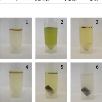
The conditions and results are shown in Table 1, and the appearance of the aqueous and organic phases for the various conditions is shown in Figure 2.

The control reaction with only KOH, NaOCl, and thymol

(Table 1, entry 1) had a colorless aqueous phase and a brown

organic phase. The latter appeared after the addition of thymol,

presumably due to decomposition in 80

C KOH solution.

(3)

In another reaction (entry 2), NH

3

(100 μ L, 28 wt%) was directly added to the hot reagent mixture. This led to yellow discoloration of the aqueous phase, with a blue color observed in the organic phase, as expected in the presence of NH

3

.

Pieces of a 5.08 cm molecular beam epitaxy (MBE)-grown bulk GaN substrate wafer were added to the reagent mixture for the third reaction (entry 3). No blue color was visible in the organic phase. The addition of ground MBE GaN (entry 4) also did not lead to a blue organic phase, though the aqueous phase had a slightly yellow color in both cases.

The MBE GaN samples had a low etch rate due to saturation of the N-face with f10¯1 ¯1g pyramids prior to etching. Polished bulk MOCVD-grown GaN was used (entry 5) to achieve a higher etch rate. Due to the polishing process, the initial GaN N-face was terminated by the quickly etched ð000¯1Þ crystal facet. This experiment (entry 5) appears essentially the same as the control experiment (entry 2) to which NH

3

was added directly. NH

3

for- mation was thus con fi rmed by the Berthelot reaction, at least in the case of GaN etching at the etch rate achieved by the polished MOCVD GaN sample. It seems likely that the sensitivity of the experimental design was too low to also detect the small concentrations of NH

3

formed by slower etching reactions (i.e., that of MBE GaN).

2.1.2. Molecular Reaction Mechanism

The formation of NH

3

during the etch reaction was con fi rmed by the three experiments described to this point. This allowed the previously reported reaction mechanisms to be narrowed to two alternatives

2GaN þ 3H

2

O ! Ga

2

O

3

þ 2NH

3

(5)

GaN þ 3H

2

O ! GaðOHÞ

3

þ NH

3

(6)

At this point, the only difference between both mechanistic approaches is the gallium – oxygen species formed. Nucleophilic attack of hydroxide ions in the solution on positively charged Ga atoms is a feasible fi rst reaction step, and has been previously reported to create Ga ─ OH bonds.

[16]

It has also been reported that Ga(OH)

3

dissolves readily in acidic and alkaline solutions, with formation of [Ga(H

2

O)

6

]

and [Ga(OH)

4

]

, respectively.

[25]

Figure 1. Images of wet pH indicator stripes placed above aqueous KOH solution (20 mL, 30 wt%) a) without and b) with polished MOCVD GaN samples. The samples were prepared at room temperature, closed, and slowly heated to 50

C. NH

3

formed by the etching reaction evaporated from the solution and caused a pH change from 7 to 12 in the vials containing GaN. The control experiments without GaN showed no pH change, proving that KOH did not evaporate.

Table 1. Berthelot reaction experiments for NH

3

detection in aqueous KOH solution at 80

C. All entries contained KOH (20 mL, 30 wt%), NaOCl solution (100 μL), and 10 mg thymol (spatula tip).

Entry NH

3

[ μ L] GaN/Si sample Appearance aqueous phase

Appearance organic phase

1 – – Colorless Brown

2 100 – Yellow Blue

3 – 5.08 cm GaN pieces Yellow Brown

4 – 5.08 cm GaN ground Yellow Brown

5 – Polished MOCVD GaN Yellow Blue

6 – Si substrate Colorless Brown

Figure 2. Images of Berthelot reaction entries 1 – 6 for detection of NH

3

during GaN etching. In all entries, KOH (20 mL, 30 wt%) was preheated

to 80

C. Thereafter, NaOCl solution (100 μ L) and 10 mg thymol (spatula

tip) were added. The entry numbers refer to Table 1. A blue organic phase

on top of the aqueous solution was observed for the polished epitaxial

GaN sample as well as the control experiment, in which exogenous

NH

3

was added to the KOH solution.

(4)

Ga

2

O

3

is generally formed from Ga(OH)

3

by dehydration.

[25]

The formation of Ga

2

O

3

would, therefore, require further reaction after the initial formation of Ga ─ OH bonds, which would not be feasible due to the solubility of Ga(OH)

3

in water.

Of the Ga species present in solution, only [Ga(OH)

4

]

is present at high pH. Thus, the net reaction of GaN etching at the reaction conditions applied in this study must be

GaN þ 3H

2

O þ OH

! GaðOHÞ

4

þ NH

3

(7) The step-by-step removal of GaN, in cycles of Ga ─ O bond formation and dissolution of the reaction products, has been extensively discussed in previous studies.

[16,22,26]

At this point, it must be clari fi ed that the postulated reaction mechanism was found under these speci fi c conditions;

other mechanisms are possible under other conditions. For instance, diffusion limitation has been reported under PEC conditions.

[17,27,28]

It is possible that the reaction mechanism changes once holes are generated by above-bandgap illumina- tion. Further experiments regarding the reaction mechanism

should include a detailed study of the transition between NH

3

formation and N

2

/H

2

formation.

2.2. Explanation for Anisotropic Etching at the Atomic Level The root cause for the development of pyramids during KOH etching was investigated at the atomic level.

2.2.1. Characterization of Pyramid Side Facet Species

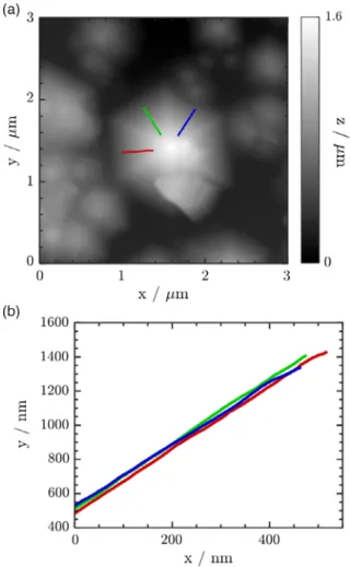
AFM measurement was applied to precisely determine the species of formed pyramid side facets as a fi rst step toward explaining the anisotropic etch behavior of GaN. The angle between the side facets and the lateral ð000¯1Þ N-face was deter- mined to be 61.5 0.6

by AFM (Figure 3).

Based on the lattice constants of wurtzite GaN, the theoretical angle between f10¯1 ¯1g and ð000¯1Þ crystal facets is 62.1

; thus, the theoretical and actual angles were in good agreement. This result indicates that the pyramid side facets represent the f10¯1 ¯1g planes.

2.2.2. Selectivity of N-Face over Ga-Face Etching

GaN reacts under dissociative water adsorption once it is immersed in aqueous KOH.

[17]

Protons bond to the negatively charged nitrogen, whereas the Ga-polar surface is terminated by hydroxide ions. The schematic surface states of both polarities are shown in Figure 4, where the Ga ─ N, Ga ─ O, O ─ H, and N ─ H bond lengths are pictured to scale with the literature values of 1.96, 1.92, 0.98, and 1.01 Å, respectively.

[29–37]

Figure 3. a) AFM image of single MOCVD GaN pyramid after 6 min in aqueous KOH solution (30 wt%) at 80

C. b) The three lines indicate the cross sections of the pyramid side facets. Height diagram of the cross sections. The angle of the side facets relative to the base plane was determined to be 61.5 0.6

, which aligns well with the theoretical angle of 62.1

, which f10¯1 ¯1g facets form with the base plane.

Figure 4. a) Schematic surfaces of Ga-polar ð0001Þ and b) N-polar ð000¯1Þ

crystal polarities on the atomic level. The top face of each schematic

represents the surface. Hydroxide ions are adsorbed to the Ga-polar

surface, whereas protons bond to nitrogen, a phenomenon referred to

as dissociative water adsorption. Black, blue, red, and white spheres

represent Ga, N, O, and H, respectively. Surface-standing free electron

pairs are indicated as orangish ellipses.

(5)

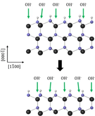
Before etching begins, the fi rst layer of Ga atoms is easily accessible to hydroxide ions in solution. The reaction mechanism established in this work means the fi rst Ga atom layer is then removed, meaning hydroxide ions are blocked by the now- exposed NH

2

groups (Figure 5, bottom).

NH

2

groups protrude at a vertical 90

angle from the Ga-polar surface. This concept of hydroxide repulsion has been previously reported.

[11]

Brie fl y, the two hydrogen atoms present on every nitrogen provide steric blocking, and the free electron pair on each nitrogen provides electronic blocking. In contrast, the initial N-polar surface is terminated with NH groups (Figure 6, top).

The nitrogen atoms on the surface bond to only one hydrogen, and do not have a free electron pair. This decreases the blocking of the Ga-polar crystal surface. The angle between the Ga ─ N bond and the lateral N-face is only 19

, compared with 90

for the Ga-face. In consequence, hydroxide ions can attack Ga, as shown in Figure 6, bottom. Once an entire GaN layer is removed, the initial surface condition present prior to etching removal is recovered. Etching of N-face GaN can thus proceed at a higher rate.

2.2.3. Stability of Pyramid Side Facets

Etch selectivity between Ga- and N-face GaN was further examined in terms of the stability of semipolar f10¯1 ¯1g pyramid

side facets. The formation of hexagonal pyramids is a conse- quence of a higher stability of the f10¯1 ¯1g crystal facets compared with the N-polar ð000¯1Þ plane. The pyramid facets were theoreti- cally investigated to examine the surface termination on the atomic level (Figure 7).

The NH

2

groups protrude from the surface with alternating angles of 79

and 35.5

. Therefore, the magnitude of the blocking against approaching hydroxide ions was expected to fall between that of the Ga- and N-faces. This relative etch selectivity conforms to the empirically observed etch behavior.

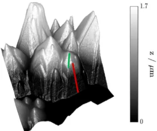
During etch experiments performed with N-polar and polished MOCVD GaN, additional crystal facets were observed

Figure 5. Removal of a single Ga atom layer from the Ga-polar ð0001Þ GaN surface results in the termination of the remaining surface, with NH

2

groups protruding at a 90

angle relative to the lateral Ga-face. Approaching negatively charged hydroxide ions are blocked by steric and electronic repulsion from negatively polarized NH

2

groups.

In addition to the two hydrogen atoms on every protruding nitrogen atom, a nonbonding electron pair is also present, providing further electronic hindrance.

Figure 6. Removal of a single GaN atom layer from the N-polar ð000¯1Þ GaN surface results in the termination of the remaining surface with NH groups protruding at a 19

angle relative to the lateral N-face.

Approaching negatively charged hydroxide ions are blocked less effectively than when approaching the Ga-face, which leads to material removal during etching.

Figure 7. Schematic surface of f10¯1 ¯1g pyramid side facets. NH

2

groups

protrude from the surface at alternating angles of 79

and 35.5

. This

situation implies relative etch selectivity between N-face and Ga-face

GaN in good agreement with actual etch behavior.

(6)

on top of f10¯1 ¯1g pyramids at a lower angle toward the lateral N-face in some cases (Figure 8, green cross section).

An angle of 38.2

0.7

relative to the lateral N-face was deter- mined. Considering the 30

rotation of the additional crystal facets in the lateral direction, the f1¯21¯4g crystal facets were identi fi ed to represent the observed angle with a theoretical value of 39.2

. The latter angle was calculated from theoretical GaN crystal lattice parameters.

In the schematic view of this crystal facet, a terraced structure was obvious with alternating situations discussed in Section 2.2.2 for ð000¯1Þ and f10¯1 ¯1g facets (Figure 9).

While etching is fast on the horizontal ð000¯1Þ N-face plateaus, the effective hydroxide blocking by NH

2

groups in the angled sections, reminiscent of the f10¯1 ¯1g situation, slows the com- bined etch rate. Thus, the expected etch selectivity of the f1¯21¯4g crystal facets was between the observed etch rates of the ð000¯1Þ and f10¯1 ¯1g facets. In fact, this theoretical consider- ation was borne out by actual etch experiments; it appears

that the f1¯21¯4g facets develop as an intermediate step if etching of an initial ð000¯1Þ GaN surface evolves into f10¯1 ¯1g pyramids.

2.2.4. Stability of Nonpolar Crystal Facets

In the next step, the etch behavior of the nonpolar f1¯100g crystal facets was analyzed (Figure 10).

Alternating NH

2

and NH groups protrude at angles of 81

and 0

, respectively. The expected relatively low etch rate was con fi rmed by scanning electron microscopy (SEM) analysis of a ground MBE GaN sample (Figure 11).

SEM images of the ground GaN powder were taken before (Figure 11a,b) and after (Figure 11c,d) etching in aqueous KOH (30 wt%) for 120 min at 80

C. The long etch time was chosen to reach termination of the GaN particles with the most stable crystal facets. Small particles of powder present prior to etching were entirely dissolved during the etching process.

Large particles within the powder showed smooth and de fi ned crystal facets after etching, and the crystal facets were arranged in terraces. The most stable GaN facets could be identi fi ed at higher magni fi cation (Figure 12).

On the bottom of the GaN particle shown, the N-polar direc- tion was identi fi ed using the large f10¯1 ¯1g pyramids. These pyr- amids transitioned into nonpolar f1¯100g facets and terminated at Ga-polar ð0001Þ crystal facets at a 90

angle. No other crystal planes were found at this point of the etch progress, proving that these three facets are indeed the most stable to KOH etching.

The three could be ranked in terms of relative etch selectivity:

the Ga-polar ð0001Þ facet has been frequently reported to show no detectable etch progress under the process conditions applied.

[10]

The etch rate of f1¯100g facets must be higher com- pared with f10¯1 ¯1g pyramid side planes. If the latter selectivity were reversed, GaN pillars would form as a consequence of N-face GaN etching instead of pyramids. In this case, some sur- face sections would have to show areas in which the f10¯1 ¯1g fac- ets transition into vertical f1¯100g facets due to a hypothetical higher resistance to etching. As this has not been observed during GaN etching under non-PEC conditions, the f10¯1 ¯1g pyramids must have higher resistance to etching. The relative Figure 8. AFM measurement of N-polar MOCVD GaN sample after

etching in aqueous KOH solution (30 wt%) at 80

C for 6 min. The red line marks a cross section of a regular f10¯1 ¯1g pyramid side facet. The green line indicates the presence of an additional set of crystal planes with an orientation rotated 30

.

Figure 9. Schematic surface of f1¯21¯4g pyramid side facets. The situation is reminiscent of a terraced combination of alternating f10¯1 ¯1g and ð000¯1Þ surface states, leading to expectation of an etch selectivity between that of ð000¯1Þ and f10¯1 ¯1g facets.

Figure 10. Schematic surface of f1¯100g GaN surface. NH

2

groups pro-

trude with an angle of 81

relative to the f1¯100g surface, whereas NH

groups provide additional blocking with a 0

angle relative to the surface.

(7)

susceptibility of the three most stable crystal facets can thus be determined to be f1¯100g > f10¯1 ¯1g > ð0001Þ. Compared with these, the N-polar ð000¯1Þ facet disappears after a relatively short period of etching. The empirically observed stability agrees with the theoretical considerations discussed by means of schematic GaN surface models on the atomic level.

2.2.5. Instability of Pyramid Tips during Prolonged Etching Etching of N-polar GaN in aqueous KOH solution has previously been reported to occur in a steady equilibrium of pyramid formation, coalescence, and erosion of the pyramid tips.

[20]

The breakdown of pyramid tips again leads to the formation of smaller pyramids. Thus, the most stable particle morphology during etching is expected to have large and smooth crystal fac- ets, and a lower relative etch resistance is expected at transitions from one facet to another. Thus, the pyramid size should become as large as possible to provide the highest possible stability.

However, during etch experiments, pyramids were found to be eroded after etching for no more than 2 min. SEM analysis of an N-polar MOCVD GaN sample surface section in 1 min steps during etching (aqueous KOH solution [30 wt%] at 80

C) showed the growth and breakdown of a large pyramid (Figure 13).

The relative instability of pyramid tips was further analyzed schematically (Figure 14).

While the pyramid side walls are formed by the stable f10¯1 ¯1g crystal facets, the tip is equivalent to a microscopic ð000¯1Þ N-face plateau. Thus, the tendency of the material to form large homo- geneous crystal facets is disrupted. During etching, the combi- nation of formation and breakdown of large crystal facets leads to a steady but slow increase in average pyramid size, a fi nding in agreement with several previous reports.

[12,20,21]

3. Conclusions

In this study, we investigated the GaN etch process in aqueous KOH solution in detail. First, the molecular reaction mechanism was elucidated using three independent experimen- tal approaches to prove that NH

3

evolves during etching.

This allowed the mechanism in aqueous solution under the speci fi c reaction conditions applied to be narrowed down to one possibility. By changes in the electrostatics of the crystal by application of bias voltage and above-bandgap illumination Figure 11. SEM images of ground MBE-grown bulk GaN particles a,b) before and c,d) after etching in aqueous KOH solution (30 wt%) at 80

C for 120 min. Small particles were entirely dissolved during etching. The remaining larger particles have smooth crystal facets arranged in terraces.

Figure 12. High magnification SEM image of a grinded MBE-grown bulk

GaN particle after etching in aqueous KOH solution (30 wt%) at 80

C for

120 min. The N-polar crystal direction is visible on the bottom of the

sample by means of large f10¯1 ¯1g pyramids. These terminated in nonpolar

f1¯100g crystal facets. In Ga-polar direction, f1¯100g facets ended at

terraced ð0001Þ plateaus. No other facets had remained at this stage of

etch duration.

(8)

(e.g., by PEC etching), the mechanism might change to a com- bination of N

3

oxidation and H

þ

reduction ─ equivalent to the concept of anodic dissolution of other common semiconductors.

The underlying reasons for the observed anisotropic etch behavior of GaN were analyzed at the atomic level. Based on the- oretical and schematic considerations, the concept of hydroxide repulsion by protruding nitrogen established in the literature was further examined. The etch selectivity of the most stable GaN crystal facets could be explained. Etching of grinded MBE-grown bulk GaN led to the conclusion that the most stable crystal facets against KOH etching are f1¯100g < f10¯1 ¯1g < ð0001Þ.

The observed breakdown of pyramid tips can be explained by the presence of a microscopic N-face ð000¯1Þ plateau with a relatively high etch rate on each pyramid tip. While the stability of the GaN surface is increased by the presence of large facets, the maximum pyramid lifetime was found to be 2 min under the reaction conditions used. Etching of GaN thus occurs as a steady equilibrium of pyramid formation and breakdown, which causes

a slow and steady increase of the average pyramid size during etching. Thus, the exact positions of the pyramid tips on the surface undergo constant change.

4. Experimental Section

Materials: Selectipur grade KOH was purchased from BASF. Planar sap- phire wafers were used as growth substrates during epitaxy. Silicon wafers were purchased from Siltronic. Commercially available MBE-grown 5.08 cm bulk GaN wafers with a threading dislocation density of 2.0 10

6

cm

2

were used. Indicator strips for pH were purchased from Roth. GPR Rectapur grade NaOCl (14 wt% active Cl

2

in aqueous solution) and ana- lytical grade thymol were used as received from VWR. BOE solution with HF (4.15 wt%) and NH

4

F (33 wt%) and no surfactants or additives was obtained from Honeywell.

Preparation of Epitaxial GaN Samples: Standard c-plane oriented GaN epilayers were grown using commercially available Veeco MOCVD tools.

After deposition of a thin AlN nucleation layer, a 3 μm bulk GaN layer was deposited in the Ga-polar direction. The dislocation density was deter- mined by photoluminescence microscopy (PLM) to be approximately 4 10

8

cm

2

. Due to the high dislocation density, this value represents a minimum, as PLM images showed dislocation aggregation.

[23]

For PLM analysis, a rudimentary GaN/In

x

Ga

1–x

N MQW was deposited on the GaN, though these wafers were not used for the etch experiments discussed later.

After epitaxial growth, the Ga-face of the epilayer was bonded to a sili- con substrate with a nonohmic metal contact to achieve electrical isolation and thus avoid substrate in fl uence on the etch process. The sapphire was removed by LLO to reveal the N-polar ð000¯1Þ crystal facet. The silicon back of the wafers was protected against KOH etching by deposition of a 20 nm Pt layer.

A set of samples underwent surface polishing; LLO surface roughness was removed using a commercially available wafer polisher. An aqueous alkaline slurry (pH 12.3) was used in combination with a mechanical com- ponent based on SiO

2

particles. This process decreased surface roughness (R

q

) from 24.1 to 1.1 nm, as measured by AFM.

Etching: Etching was conducted with full 15.24 cm MOCVD GaN wafers, with cut samples with dimensions of 1 2 cm, and with commer- cially available MBE-grown bulk GaN samples. Etching of 15.24 cm GaN wafers was conducted in a beaker. The wafers were placed on Teflon place Figure 13. Consecutive SEM images of the same surface of a MOCVD-grown N-face GaN etched in 1 min steps in aqueous KOH solution (30 wt%) at 80

C. The observed pyramid had grown to its maximum size in the fourth image. After 1 min prolonged etch time, the tip of the pyramid had broken down, leading to the development of smaller pyramids.

Figure 14. Schematic tip of f10¯1 ¯1g GaN pyramid on the atomic level.

Directly on the tip, a microscopic ð000¯1Þ is visible. This explains the

relative instability of the pyramid tip, which leads to the breakdown of

large pyramids.

(9)

holders to allow for magnetic stirring underneath the wafer. Etching of cut 1 2 cm MOCVD GaN sample pieces, as well as ground or fragmented MBE bulk GaN, was conducted in 50 mL polypropylene centrifuge vials under magnetic stirring. The KOH solution was heated to the process tem- perature prior to immersion of the wafer to enable maintenance of a stable process temperature over the entire etch period.

Analytical Methods: PLM images were recorded directly after epitaxy using an Olympus BX51 microscope with an Olympus U-RFL-T UV light source. Light with a wavelength of 408 nm was used for excitation. AFM measurements were taken using a Veeco/Bruker microscope and a Scanasyst-Air tip with a 2 nm diameter. All measurements were recorded in peak force tapping mode at 2 kHz. SEM images were recorded on a Zeiss Gemini Leo 1530 microscope with an acceleration voltage of 2 keV and SE2 detection.

Acknowledgements

This work was funded by OSRAM Opto Semiconductors GmbH. The authors thank all colleagues at OSRAM Opto Semiconductors GmbH for contributing to the success of the experiments reported here.

D.D.D. thanks Deutsche Forschungsgemeinschaft (DFG) for the Heisenberg Professorship Award and the Spanish Ministry of Science, Innovation and Universities for the Senior Beatriz Galindo Award (Distinguished Researcher; BEAGAL18/00166). D.D.D. thanks NANOtec, INTech, Cabildo de Tenerife, and ULL for laboratory facilities. Open access funding enabled and organized by Projekt DEAL.

Conflict of Interest

The authors declare no conflict of interest.

Keywords

anisotropy, etching, gallium nitride, light-emitting diodes, mechanism Received: April 15, 2020 Revised: August 4, 2020 Published online: September 10, 2020

[1] S. Nakamura, Angew. Chem. Int. Ed. 2015, 54, 7770.

[2] H. C. Yang, T. Y. Lin, Y. F. Chen, Phys. Rev. B 2000, 62, 12593.

[3] S. Nakamura, M. Senoh, N. Iwasa, S. Nagahama, Jpn. J. Appl. Phys.

1995, 34, L797.

[4] S. Nakamura, Y. Harada, M. Seno, Appl. Phys. Lett. 1991, 58, 2021.

[5] L. Liu, J. H. Edgar, Mater. Sci. Eng. R 2002, 37, 61.

[6] J. J. Wierer, D. A. Steigerwald, M. R. Krames, J. J. O’Shea, M. J. Ludowise, G. Christenson, Y.-C. Shen, C. Lowery, P. S. Martin, S. Subramanya, W. Götz, N. F. Gardner, R. S. Kern, S. A. Stockman, Appl. Phys. Lett. 2001, 78, 3379.

[7] A. David, T. Fujii, B. Moran, S. Nakamura, S. P. DenBaars, C. Weisbuch, H. Benisty, Appl. Phys. Lett. 2006, 88, 133514.

[8] W. S. Wong, T. Sands, N. W. Cheung, M. Kneissl, D. P. Bour, P. Mei, L. T. Romano, N. M. Johnson, Appl. Phys. Lett. 1999, 75, 1360.

[9] Y. Jung, J. Ahn, K. H. Baik, D. Kim, S. J. Pearton, F. Ren, J. Kim, J. Electrochem. Soc. 2012, 159, H117.

[10] M. Tautz, D. Díaz Díaz, ChemistrySelect 2018, 3, 1480.

[11] D. Zhuang, J. H. Edgar, Mater. Sci. Eng. R 2005, R 48, 1.

[12] H. M. Ng, N. G. Weimann, A. Chowdhury, J. Appl. Phys. 2003, 94, 650.

[13] W. Guo, R. Kirste, I. Bryan, Z. Bryan, L. Hussey, P. Reddy, J. Tweedie, R. Collazo, Z. Sitar, Appl. Phys. Lett. 2015, 106, 082110.

[14] T. Kozawa, T. Kachi, T. Ohwaki, Y. Taga, N. Koide, M. Koike, J. Electrochem. Soc. 1996, 143, L17.

[15] S. J. Pearton, J. J. Chen, W. T. Lim, F. Ren, D. P. Norton, ESC Trans.

2007, 6, 501.

[16] D. Li, M. Sumiya, S. Fuke, D. Yang, D. Que, Y. Suzuki, Y. Fukuda, J. Appl. Phys. 2001, 90, 4219.

[17] J. M. Hwang, J. T. Hsieh, C. Y. Ko, H. L. Hwang, W. H. Hung, Appl. Phys. Lett. 2000, 76, 3917.

[18] D. R. Turner, J. Electrochem. Soc. 1960, 107, 810.

[19] C. Youtsey, I. Adesida, G. Bulman, Appl. Phys. Lett. 1997, 71, 2151.

[20] S.-C. Han, J.-K. Kim, J. Y. Kim, K.-K. Kim, H. Tampo, S. Niki, J.-M. Lee, J. Electrochem. Soc. 2010, 157, D60.

[21] T. Palacios, F. Calle, M. Varela, C. Ballesteros, E. Monroy, F. B. Naranjo, M. A. Sánchez-García, E. Calleja, E. Mu noz, ˜ Semicond. Sci. Technol. 2000, 15, 996.

[22] M. Itoh, T. Kinoshita, C. Koike, M. Takeuchi, K. Kawasaki, Y. Aoyagi, Jpn. J. Appl. Phys. 2006, 45, 3988.

[23] M. Tautz, M. T. Kuchenbrod, J. Hertkorn, R. Weinberger, M. Welzel, A. Pfitzner, D. Díaz Díaz, Beilstein J. Nanotechnol. 2020, 41.

[24] C. J. Patton, S. R. Crouch, Anal. Chem 1977, 49, 464.

[25] A. F. Holleman, E. Wiberg, N. Wiberg, Lehrbuch Der Anorganischen Chemie, De Gruyter, Berlin, Germany 2007.

[26] S.-R. Xu, Y. Hao, J.-C. Zhang, X.-W. Zhou, Y.-R. Cao, X.-X. Ou, W. Mao, D.-C. Du, H. Wang, Chin. Phys. B 2010, 19, 107204.

[27] J. I. Pankove, J. Electrochem. Soc. 1972, 119, 1118.

[28] E. Harush, S. Brandon, J. Salzman, Y. Paz, Semicond. Sci. Technol.

2002, 17, 510.

[29] H. Morkoç, Handbook of Nitride Semiconductors and Devices, Wiley-VCH, Weinheim, Germany, 2008.

[30] Y. Zhau, J. Davis Jr., C. S. Day, A. Lachgar, Structural Complexity and Dimensional Flexibility of Gallium Dialkylphosphonates, John Wiley &

Sons, Inc., New York 2012.

[31] M. Marezio, J. P. Remeika, J. Chem. Phys. 1967, 46, 1862.

[32] S. Singh, V. Jancik, H. W. Roesky, R. Herbst-Irmer, Inorg. Chem. 2006, 45, 949.

[33] W. C. Hamilton, Acta Cryst. 1962, 15, 353.

[34] S. F. Rastegar, A. A. Peyghan, H. R. Ghenaatian, N. L. Hadipour, Appl. Surf. Sci. 2013, 274, 217.

[35] L. Zhang, Y. Shao, Y. Wu, X. Hao, X. Chen, S. Qu, X. Xu, J. Alloys Compd. 2010, 504, 186.

[36] P. Visconti, K. M. Jones, M. A. Reshchikov, R. Cingolani, H. Morkoc, R. J. Molnar, Appl. Phys. Lett. 2000, 77, 3532.

[37] A. Botti, F. Bruni, S. Imberti, M. A. Ricci, A. K. Soper, J. Mol. Liq. 2005,

117, 81.

Abbildung

Figure 2. Images of Berthelot reaction entries 1 – 6 for detection of NH 3
Figure 3. a) AFM image of single MOCVD GaN pyramid after 6 min in aqueous KOH solution (30 wt%) at 80  C
Figure 5. Removal of a single Ga atom layer from the Ga-polar ð0001Þ GaN surface results in the termination of the remaining surface, with NH 2 groups protruding at a 90  angle relative to the lateral Ga-face
Figure 9. Schematic surface of f1¯21¯4g pyramid side facets. The situation is reminiscent of a terraced combination of alternating f10¯1 ¯1g and ð000¯1Þ surface states, leading to expectation of an etch selectivity between that of ð000¯1Þ and f10¯1 ¯1g fac
+3

Referenzen

ÄHNLICHE DOKUMENTE

Reflection high-energy electron diffraction (RHEED) is established as a powerful tool in MBE, and is routinely used to investigate growth mode, growth rate, flatness, crystal

Speziell die drei letzten bilden eine thermodynami- sche Stabilitätsfolge; man erhält nämlich aus Per- chlorcyclooctatetraen (y-C8Cl8) je nach dem Grad des

schon diese Stellen scheinen mir genügend zu erweisen, daß es sich. im Suttanipäta um einen jnitw/a-Gürtel handelt, und

Between these two apparatuses a homogenous magnetic field is applied in y-direction, giving rise to a precession of the spin during the time of flight T from the first to the

It was quite dark when the door which communicated with the corridor opened, and Agmahd entered, followed by a young priest, who brought me food and a cup of some strange sweet-.!.

M.. Proposed models, algorithms.. c ) Mapping of economic damage. d ) Calculation of fields of pollutant maximum concentrations under normal un- favorable

The structure of the title complex appears to rep- resent an intermediate state between a fully ionic ex- treme with linearly two-coordinate silver in a cation [RNCAgCNR] +

Given the dramatic increase in artificial light in recent years, we see an urgent need for research on the physiological, human health, ecological, and