superconducting coplanar resonators:
Materials, nano-electromechanics, and few-electron systems
Dissertation
zur Erlangung des Doktorgrades der Naturwissenschaften (Dr. rer. nat) der Fakultät Physik der Universität Regensburg
vorgelegt von
Peter Stiller
aus Laub
unter Anleitung von Dr. Andreas K. Hüttel
Januar 2016
Das Promotionsgesuch wurde am 26.10.2015 eingereicht.
Das Kolloquium fand statt am 06.04.2016.
Die Arbeit wurde von Dr. Andreas K. Hüttel angeleitet.
Prüfungsausschuss: Vorsitzender: Prof. Dr. Klaus Richter
1. Gutachter: Dr. Andreas K. Hüttel
2. Gutachter: Prof. Dr. Jascha Repp
weiterer Prüfer: Prof. Dr. Rupert Huber
Contents
List of Figures viii
List of Tables ix
List of Symbols x
1 Introduction 1
2 Fundamental electronic properties of carbon nanotubes 5
2.1 Carbon nanotube lattice . . . . 6
2.2 Carbon nanotube band structure . . . . 8
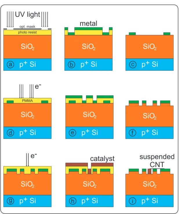
3 Fabrication and measurement techniques for CNT devices 13 3.1 Fundamental nanofabrication techniques . . . . 15
3.2 Electrode geometry for the carbon nanotube overgrowth . . . . . 17
3.3 Room temperature characterization . . . . 17
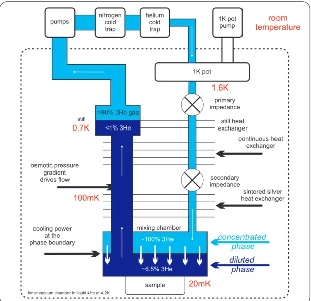
3.4 The dilution refrigerator . . . . 20
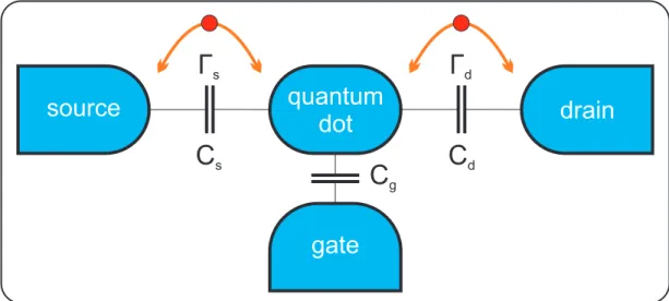
4 Electronic transport through CNT quantum dots 23 4.1 Quantum dots . . . . 24
4.2 Carbon nanotube quantum dots . . . . 27
4.3 Quantum dot transport spectroscopy . . . . 28
5 Carbon nanotubes in a parallel magnetic field 33 5.1 Carbon nanotube single particle spectrum . . . . 34
5.2 Quantum mechanical transmission . . . . 38
5.3 Transmission calculations for different kinds of CNTs . . . . 40
5.4 Magnetic field dependence of k k . . . . 45
iv
6 Magnetic field induced electron-vibron coupling 53
6.1 Vibrational modes in carbon nanotubes . . . . 54
6.2 Franck-Condon model . . . . 56
6.3 Magnetic field induced coupling . . . . 58
6.4 Physical origin of the magnetic field induced coupling . . . . 62
7 Negative frequency tuning of a CNT mechanical resonator 65 7.1 Mechanical properties of suspended, doubly clamped CNTs . . . . 66
7.2 Gate tuning of mechanical resonance . . . . 67
7.3 Measurement setup and detection technique . . . . 68
7.4 Electronic device characterization . . . . 68
7.5 Driven mechanical resonator . . . . 71
7.6 Negative frequency tuning . . . . 72
8 Coplanar waveguide resonators for CNT integrated circuits 77 8.1 Device fabrication . . . . 78
8.2 Microwave frequency measurement setup . . . . 81
8.3 Quality factor evaluation . . . . 83
8.4 Characterization of niobium quarter wavelength resonators . . . . 85
8.5 Two-level system loss in CPWs . . . . 88
8.6 Matthis Bardeen theory for CPWs . . . . 95
8.7 Calculating the kinetic inductance fraction . . . . 97
8.8 Combining CNT and CPW . . . . 98
9 Conclusions and outlook 103 A Fabrication details and recipes 107 A.1 Carbon nanotube quantum dot devices . . . . 107
A.2 Coplanar waveguide fabrication . . . . 112
B Calculating a theoretical value β 114 C Numerical transmission calculations of carbon nanotubes 116 C.1 Hopping integrals . . . . 116
C.2 Additional transmission calculations . . . . 117
D Coplanar waveguide parameters 120 D.1 Calculation of the effective permittivity . . . . 120
D.2 Resonant and relaxation susceptibility tensors . . . . 122
E HF measurement technology 124
List of Figures
2.1 Definition of carbon nanotube chiral vector and translation vector 7
2.2 Tight binding calculation of graphene dispersion relation . . . . . 9
2.3 Tight binding calculation of carbon nanotube band structures . . 11
3.1 Device fabrication for overgrown carbon nanotubes . . . . 14
3.2 Carbon nanotube growth setup . . . . 16
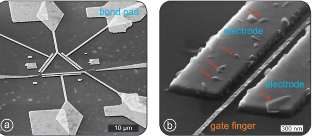
3.3 SEM image of overgrown carbon nanotubes . . . . 18
3.4 Device geometry for rhenium contact electrodes . . . . 19
3.5 SEM image of the device geometry for rhenium and molybdenum alloys . . . . 19
3.6 Carbon nanotube room temperature characterization . . . . 20
3.7 Functionality of a dilution refrigerator . . . . 21
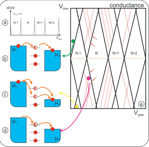
4.1 Sketch of a quantum dot and its coupling to the environment . . . 24
4.2 Single electron transport through a quantum dot . . . . 26
4.3 Band structures at the carbon nanotube-metal interface . . . . 28
4.4 Sketch of the conductance as a function of both gate voltage and bias voltage . . . . 30
4.5 Current and conductance measurements as function of gate voltage and bias voltage . . . . 31
5.1 Dispersion relation near the K and K 0 points . . . . 36
5.2 Comparison of the measured carbon nanotube single particle spec- trum and an analytic model . . . . 37
5.3 Calculated transmission for a (5, 2) carbon nanotube . . . . 42
5.4 Calculated transmission for a (29, 20) carbon nanotube . . . . 44
5.5 Magnetic field values for the Dirac point crossing as a function of the radius and the chiral angle of a carbon nanotube . . . . 45
vi
5.7 Magnetic field values for the Dirac point crossing as a function of
the length of a carbon nanotube . . . . 47
5.8 Dependence of the momentum shift k k on the momentum shift k ⊥ 48 5.9 Comparison of numerical transmission calculations and an analytic model . . . . 51
6.1 Vibrational modes in carbon nanotubes . . . . 55
6.2 Poisson distribution for the Franck-Condon model . . . . 58
6.3 Current and conductance as a function of both bias voltage and parallel magnetic field . . . . 59
6.4 Traces of the conductance and the current as a function of bias voltage for constant parallel magnetic field . . . . 60
6.5 Electron-vibron coupling factor as function of a parallel magnetic field . . . . 60
6.6 Conductance as a function of both bias voltage and parallel mag- netic field . . . . 62
6.7 Comparison of two different methods to obtain the electron-vibron coupling parameter . . . . 63
6.8 Maximal current of the ground state as a function of a parallel magnetic field . . . . 64
7.1 Low temperature measurement setup . . . . 69
7.2 Photograph of the contact-free cryogenic antenna . . . . 70
7.3 Room temperature conductance measurement . . . . 70
7.4 Low temperature conductance measurement . . . . 71
7.5 Conductance as function of both gate voltage and bias voltage displaying the so-called Coulomb diamond stability diagram . . . 72
7.6 Current as a function of the applied radio frequency . . . . 73
7.7 Negative frequency tuning of a carbon nanotube mechanical oscil- lator . . . . 74
8.1 SEM image of the coplanar waveguide design . . . . 79
8.2 Critical temperature of niobium . . . . 80
8.3 Photograph of the used sample holder system . . . . 81
8.4 Photograph of our dilution system and microwave setup . . . . 82
8.5 Photograph of the HEMT amplifier and the circulator . . . . 83
8.6 |S 21 | 2 transmission of a niobium coplanar waveguide resonator . . 85
8.7 Characterization of a niobium resonator at 4 K . . . . 86
8.8 Temperature dependence of a resonance feature of a niobium copla-
nar waveguide resonator . . . . 87
Contents viii
8.9 Internal quality factor of a niobium coplanar waveguide resonator as a function of temperature . . . . 88 8.10 Resonance frequency of a niobium coplanar waveguide resonator
as a function of temperature . . . . 89 8.11 Two-level system fit for a niobium coplanar waveguide resonator . 92 8.12 Power dependence of two-level system loss in a niobium coplanar
waveguide resonator . . . . 94 8.13 Matthis Bardeen fit for a niobium coplanar waveguide resonator . 96 8.14 Room temperature conductance measurement . . . . 100 8.15 SEM image of a potential sample design for combining carbon
nanotubes and coplanar waveguide resonator . . . . 101 B.1 Height dependence of the second derivative C gate 00 . . . . 115 C.1 Coordinates for the hopping integrals . . . . 117 C.2 Calculated transmission for a (14, 11) carbon nanotube with dif-
ferent length . . . . 118
C.3 Calculated transmission through different carbon nanotubes . . . 119
D.1 Sketch for the calculation of eff . . . . 121
2.1 Solutions E(k x , k y ) = 0 of the graphene dispersion relation E(k x , k y ) 8 5.1 Extracted values of an analytic fit of the measured carbon nan-
otube single particle spectrum . . . . 38 5.2 Magnetic field values for the Dirac point crossing for different kinds
of carbon nanotubes obtained from numerically transmission cal- culations . . . . 41 8.1 Design frequencies of our coplanar waveguide resonator resonators 80 8.2 Resonance frequencies of a niobium coplanar waveguide resonator
at 4 K . . . . 86 8.3 Comparison of our results obtained by influence of two-level sys-
tems with literature . . . . 93 8.4 Comparing different qubit-photon coupling experiments . . . . 100
ix
List of Symbols
a Lattice constant of graphene (a = 2.46 · 10 −10 m) . . . . 6
~a 1,2 Unit vectors of the hexagonal graphene lattice . . . . 6
A Cross section . . . . 66
B k Parallel magnetic field . . . . 33
B min Parallel magnetic field corresponding to the Dirac point crossing . . 36
C Σ,s,d,g Total, source, drain and gate capacitances of a quantum dot . . . . 27
C ~ h Chiral vector . . . . 6
d Lead coupling parameter . . . .40
d CNT Diameter . . . . 7
d ~ Dipole moment . . . . 90
δ Spin-orbit coupling parameter . . . . 35
∆ 0 Tunnel splitting . . . .88
∆ BCS BCS energy gap . . . . 95
∆ T =0 Superconducting energy gap for T = 0 . . . . 95
δ TLS Two-level system loss tangent . . . . 91
δ TLS ∗ Effective, reduced two-level system loss tangent . . . . 91
∆ TLS Two-level system asymmetry . . . . 88
∆k ⊥ Sub-band spacing . . . . 8
∆ Energy splitting induced by charge carrier quantum confinement . . . 8
∆ KK’ KK 0 splitting . . . . 34
∆ SO Spin-orbit splitting . . . . 34
e Elementary charge, e = 1.602 · 10 −19 C . . . . 23
E Young’s modulus . . . . 66
x
E RBM Energy of the radial breathing mode . . . . 54
E SM Energy of the stretching mode . . . . 55
Eigenenergies . . . . 90
0 Vacuum permittivity ( 0 ' 8.854 · 10 −12 A s/(V m)) . . . . 67
eff Effective permittivity . . . . 78
η Linear damping . . . . 66
f design Designed resonance frequency of a CPW resonators . . . . 78
f res Measured resonance frequency of a CPW resonators . . . . 84
F Two-level system filling factor . . . . 91
F ac Time-dependent external force . . . . 67
F dc Static external force . . . . 67
F ext External force driving a carbon nanotube . . . . 66
g Electron-phonon coupling parameter . . . . 53
g g,f Geometrical factors for ground plane and CPW feedline . . . . 97
G Conductance . . . . 23
G CNT Maximal carbon nanotube conductance . . . . 23
Γ Tunneling rate . . . . 56
¯ h Reduced Planck constant, ¯ h = 6.58 · 10 −16 eVs . . . . 2
h Vertical distance height between gate and carbon nanotube . . . . 67
h 0 Equilibrium height . . . . 67
I Momentum of inertia . . . . 66
I max Maximal current at the ground state . . . . 58
k ⊥ Wave vector perpendicular to the carbon nanotube axis . . . . 9
k k Wave vector parallel to the carbon nanotube axis . . . . 8
k b Boltzmann constant, k b = 8.62 · 10 −5 eVK −1 . . . . 2
l Classical displacement of carbon nanotube lattice . . . . 56
l 0 Length scale of the quantum harmonic oscillator . . . . 56
l cpw Length of the meandering CPW resonator . . . . 78
L Length of a suspended carbon nanotube . . . . 66
L k,m Kinetic and magnetic inductance per unit length . . . . 97
λ F Fermi wavelength . . . . 26
µ Electro-chemical potential of a quantum dot . . . . 25
µ B Bohr magneton, µ B ' 5.788 · 10 −5 eV/T) . . . . 38
Contents xii
µ s,d Electro-chemical potential of source and drain . . . . 25
n, m Chiral indices . . . . 6
n s Charge carrier density of states . . . . 26
n vib Vibrational mode number . . . . 55
N Number of charge carriers . . . .25
P Output power of a RF generator . . . . 71
P generator Output power of a microwave generator . . . . 85
P in Effective input power at the sample . . . . 85
P TLS Two-level system density of states . . . .90
Φ 0 Magnetic flux quantum . . . . 33
Ψ i Vibrational wave function . . . .56
Q c Coupled quality factor . . . . 84
Q e External quality factor . . . . 84
Q i Internal quality factor . . . . 84
Q l Loaded quality factor . . . . 84
R CNT Carbon nanotube device resistance . . . . 69
ρ Mass density . . . .66
s Distance between CPW feedline and ground plane . . . . 78
S ij Scattering matrix element from port j to port i . . . . 83
σ Valley quantum number . . . . 34
σ i Pauli matrices . . . . 90
σ 1,2 Real and imaginary part of the complex conductivity . . . . 95
T Sample temperature . . . . 2
T 0 Residual tension . . . . 66
T ac Time-dependent tension . . . . 67
T c Critical temperature . . . . 78
T dc Static tension . . . . 67
T mech Tension . . . . 66
T ~ Translation vector . . . . 6
τ Spin quantum number . . . . 34
Θ Chiral angle . . . . 6
U ac Time-dependent displacement . . . .66
U dc Static displacement . . . . 66
U (z, t) Time dependent elongation . . . . 66
v F Fermi velocity . . . . 34
V i in Voltage input at port i . . . . 83
V i out Voltage output at port i . . . . 83
w Width of the CPW feedline . . . . 78
ξ res,rel Resonant and relaxation tensor . . . . 90
Z Atom number of a carbon nanotube unit cell . . . . 6
Introduction
Carbon nanotubes are a prominent carbon based nano-material. In 1952 first multi-walled carbon nanotubes were discovered in TEM images [Radushkevich and Luk’yanovich, 1952]. Subsequently, single-walled carbon nanotubes were ob- served in discharge experiments [Iijima and Ichihashi, 1993, Bethune et al., 1993].
Ongoing progress in nano-fabrication techniques lead to first measurements of sin- gle carbon nanotubes contacted to metallic leads; showing a quantum wire like transport at low temperatures [Tans et al., 1997] and transistor behavior at room temperature [Tans et al., 1998]. Further improvements of fabrication techniques and measurement setups led to a rich field of carbon nanotube physics. Nowadays carbon nanotubes can be grown defect-free directly on the substrate by chemical vapor deposition. Carbon nanotubes are intrinsic one-dimensional conductors, and the formation of a "zero-dimensional" quantum dot system is straightforward compared, e.g., to electrostatically constricting a two-dimensional electron gas.
The quantum confinement of electrons in carbon nanotubes leads to a rich spec- trum of transport phenomena; many different parameter regimes have already been observed. Carbon nanotubes display Luttinger-liquid behavior [Bockrath et al., 1999, Postma et al., 2001], show ballistic transport [Cao et al., 2005] and Fabry-Perot like oscillations in an open transport regime [Liang et al., 2001].
Carbon nanotubes can be connected to many different types of metallic leads, including ferromagnetic [Jensen et al., 2005] and superconducting materials [Mor- purgo et al., 1999].
In addition, carbon nanotubes also show excelling mechanical properties, having a low mass, high stiffness and an extremely high Young’s modulus [Lu, 1997].
They can act as mechanical beam resonators on the nano-scale [Sazonova et al., 2004], achieving high-quality factors in carbon nanotube nano-electromechanical devices [Hüttel et al., 2009a]. Recently quality factors of the mechanical bending
1
2
mode vibration of a carbon nanotube resonator up to 5 · 10 6 were demonstrated [Moser et al., 2014]. Low mass and ultimate quality factor made it possible to employ carbon nanotubes as ultra-sensitive mass sensors [Lassagne et al., 2008].
Due to their high mechanical resonance frequency of several hundreds of mega- hertz [Hüttel et al., 2009a, Stiller et al., 2013] carbon nanotubes also provide a promising system for reaching the quantum limit of mechanical motion. This re- quires k b T << hω, which can here be in principle directly reached with common ¯ dilution refrigerators.
A rather new development regarding carbon nanotubes is the integration in super- conducting microwave circuits. Coplanar waveguides (CPW) were first suggested in [Wen, 1969], here a transmission strip-line is fabricated on a dielectric substrate material. Later CPWs were used as superconducting resonators [Day et al., 2003];
the small size of CPW resonators allowed the integration in on-chip microwave circuits. In [Wallraff et al., 2004] the combination of a CPW resonator acting as an on-chip cavity and a qubit defined in a cooper pair box was presented leading to a solid state based cavity quantum electrodynamic system, a proposal first was given by [Blais et al., 2004, Childress et al., 2004]. The Cooper pair box acts as a charge qubit; its states are coupled to the electric field of the transmission line resonator. A qubit is a fully manipulable quantum mechanical two-level system;
it is the basic unit for quantum computing and quantum cryptography. The mi- crowave resonator can be employed for read-out and manipulation of the qubit quantum states. As an example, a single electron in a double quantum dot or the polarization of a single photon can act as a qubit. The experiments coupling a superconducting microwave resonator and a qubit target the fundamental inter- action of matter and light [Jaynes and Cummings, 1963, Childress et al., 2004].
The Jaynes-Cummings model describes the interaction of a two-level system and a quantized harmonic mode of an optical cavity; by using a superconducting mi- crowave resonator and an artificial atom, an analogon to a optical cavity can be achieved.
Carbon nanotubes are a common material to define single and double quan- tum dots, allowing also the formation of a charge or spin qubits; the absence of hyperfine interaction in carbon yields a large spin decoherence time in carbon nanotubes necessary for a manipulation of spin states [Fischer et al., 2009].
Recently the combination of a carbon nanotube single [Delbecq et al., 2011] and double quantum dot [Viennot et al., 2014, Viennot et al., 2015] and a half wave- length CPW resonator was presented. In carbon nanotubes the confinement of electrons is much stronger than in a two-dimensional electron gas since they are smaller in size and intrinsically one-dimensional. Furthermore carbon nanotubes can display large electric dipole moments leading to a much stronger coupling of both systems.
For the combination of carbon nanotube quantum dots and CPW resonators, a
reliable fabrication for both systems is necessary. In this thesis electronic and
mechanical experiments on clean, suspended carbon nanotubes are presented; in
addition first measurements of niobium quarter wavelength CPW resonators are shown.
This thesis starts with a short introduction of the fundamental electronic proper- ties of carbon nanotubes in chapter 2. In the following chapter 3 the fabrication process for overgrown carbon nanotube devices is explained. In addition the re- quired room temperature and low temperature measurement setups are shown.
Chapter 4 presents the basic concept of quantum dot systems in carbon nan-
otubes. Numerical transmission calculations on carbon nanotubes and the influ-
ence of a parallel magnetic field on the carbon nanotube single particle spectrum
are shown in chapter 5 with the objective to identify the chirality of a measured
carbon nanotube. The interaction of phonons and electrons in carbon nanotubes
and the influence of a magnetic field is discussed in chapter 6. Chapter 7 discusses
a specific device where an applied gate voltage enables negative frequency tuning
of the carbon nanotube mechanical resonator. Preparatory measurements on su-
perconducting quarter-wavelength resonators are shown in chapter 8, discussing
also the potential design of the combination of superconducting resonators and
carbon nanotubes. Finally the experimental results of this thesis are concluded,
and a short outlook on possible future experiments is given. Technical details to
the different chapters are additionally presented in the appendix.
Fundamental electronic properties of carbon nanotubes
In this chapter a brief overview of the fundamental properties of carbon nanotubes is given. First, the lattice quantities defining a carbon nanotube are explained.
Then the band structure in zone-folding approximation is demonstrated.
The carbon atom, foundation of all organic chemistry, has an electronic shell con- figuration of 2s 1 2s 2 2p 2 , i.e. every carbon atoms has six electrons. Particular for carbon are the well known sp, sp 2 , and sp 3 hybridizations leading to the wide field of organic chemistry; a linear combination of the 2s 2 electron and the 2p 2 elec- trons form energetically degenerate hybridized orbitals. An sp 3 hybridized carbon atom forms four covalent bonds via hybridization of the 2s orbital and the three 2p orbitals; this forms for instance diamond. The four hybridized orbitals are arranged in a tetrahedron like structure to maximize the distance between them.
Another well known carbon compound, graphite, consists of sp 2 hybridized car- bon atoms. Here the 2s orbital and two 2p orbitals form three hybridized orbitals.
These are arranged in a plane with an angle of 120 ◦ between each hybridized or- bital. This builds up a hexagonal lattice, which is sketched in figure 2.1. Graphite consists of many of these layers adhering via van-der-Waals interaction. One sin- gle layer is called graphene; a recently isolated two dimensional nano-scale mate- rial. The fabrication of single layer graphene started a new field in physics due to the excelling electronic properties of graphene [Novoselov et al., 2004]. The investigation was honored with the Nobel prize in 2010. Since that time many different researchers work on graphene. In this case of sp 2 hybridization, the third, non-hybridized p orbital of the carbon atoms in graphene forms delocal- ized π orbitals. These are responsible for the electronic transport since σ bonds are far away form the Fermi energy and do not contribute to electronic transport.
Carbon nanotubes can be imaged as rolled up graphene sheets; so it is not surpris- ing to start with the graphene lattice to derive the properties of carbon nanotubes.
5
2.1. Carbon nanotube lattice 6
2.1 Carbon nanotube lattice
Starting from graphene one can define the basic lattice parameters of carbon nanotubes. The two atom unit cell of graphene is defined by two primitive lattice vectors ~a 1 and ~a 2 (see figure 2.1) and a corresponding bond length a bond = 1.42 Å.
The resulting lattice constant reads
a = |~a 1 | = |~a 2 | = a bond √
3 = 2.46 Å. (2.1)
An important quantity for carbon nanotubes is the so-called chiral vector
C ~ h = n~a 1 + m~a 2 ; (2.2)
defining the roll-up direction for carbon nanotubes. In a thought-experiment, where a graphene sheet is rolled up into a carbon nanotube it subsequently lies along the circumference of the carbon nanotube. Together with the translation vector T ~ it defines the carbon nanotube unit cell. The translation vector reads
T ~ = 2m + n
g · ~a 1 − 2n + m
g ·~a 2 , (2.3)
with g being the greatest common divisor of (2m + n) and (2n + m). The atom number Z within one unit cell can be calculated using the vectors C ~ and T ~ ; the results is
Z = 2 · | C ~ × T ~ |
| ~a 1 × ~a 2 | . (2.4)
As one can easily see each carbon nanotube is fully described by its chiral indices n and m, see figure 2.1. The chiral angle is given by
cos(Θ) = C ~ · ~a 1
| C||~a ~ 1 | = 2n + m 2 √
n 2 + nm + m 2 (2.5)
and is defined as the angle between ~a 1 and C ~ h . The hexagonal lattice restricts the chiral angle to values between Θ = 0 ◦ and Θ = 30 ◦ .
Depending on Θ different carbon nanotube classes arise. For Θ = 0 ◦ a so-called
zigzag type carbon nanotube is obtained and for Θ = 30 ◦ the carbon nanotube is
of armchair type. Both types are so-called achiral carbon nanotubes since they
armchair direction
a 1
k
xk
yθ a 2
T
C h
x y
zigzag direction
Figure 2.1: Sketch of a graphene lattice. The carbon atoms are depicted as black dots. The two lattice vectors ~a 1 and ~a 2 , the chiral vector C ~ h and the translation vector T ~ of an exemplary (4, 2) carbon nanotube are shown. Zig-zag and armchair directions are depicted in cyan. The names arise from the shape of the circumference.
have a mirror symmetry, all other types of carbon nanotubes are called chiral.
The roll-up direction for both types is sketched in figure 2.1.
The diameter of a (n, m) carbon nanotube reads
d CNT = | C| ~
π = a √
n 2 + nm + m 2
π , (2.6)
which is typically in the range of a few nanometers. These values are the basic quantities defining the carbon nanotube lattice. To derive an approximation for the band structure and the electronic properties of a carbon nanotube one starts with the dispersion relation for the π electrons of graphene
E(k x , k y ) = ±
(
1 + 4 cos
√ 3k x a 2
!
cos k y a 2
!
+ 4 cos 2 k y a 2
!) 1/2
, (2.7)
obtained using a tight binding approximation; a more detailed discussing can be
found in [Saito et al., 1998].
2.2. Carbon nanotube band structure 8
Figure 2.2(a) shows this well-known dispersion relation of graphene. The π and π ∗ bands touch each other at the corners of the reciprocal first Brillouin zone, these corner points are labeled as K in solid state physics. Only two of the six corner points are independent in the reciprocal graphene lattice, the other points are connected by lattice vectors. In graphene and carbon nanotubes the two independent points are labeled K and K 0 . The dispersion relation becomes linear near the K and K 0 points. Graphene is a so-called zero band gap semiconductor since the density of states at the Fermi energy goes to zero; but the valence and conduction band touch each other at the K and K 0 points. Setting E(k x , k y ) = 0 one can locate the six coordinate pairs (k x a, k y a); they are listed in table 2.1.
(k x a, k y a) (k x a, k y a) (k x a, k y a)
group 1 0, − 4π 3 √ 2π 3 , π 3 − √ 2π 3 , π 3
group 2 0, + 4π 3 √ 2π
3 , − π 3 − √ 2π
3 , − π 3
Table 2.1: Solutions E(k x , k y ) = 0 of the graphene dispersion relation E(k x , k y ), only two of six points are independent in the graphene lattice, see text. The six points are marked in figure 2.2(b).
2.2 Carbon nanotube band structure
The carbon nanotube band structure can be approximated using the so-called zone-folding technique. The wave function along the carbon nanotube circumfer- ence has to fulfill a 2π periodicity, requiring
~k · C ~ h = k x a
√ 3
2 (n + m) + k y
a
2 (n − m) = 2πq (2.8) for the wave vector ~k with an integer q. The one-dimensional sub-bands are separated in momentum space by
∆k ⊥ = 2π
C ~ h . (2.9)
Note that the wave vectors k k along the carbon nanotube axis remain continu-
ous. One can see that the two-dimensional band structure of graphene this way
collapses to one dimensional sub-bands.
k x
k y
armchair zig-zag
Δk
k y k x
E
a b
K K‘
valence band
conduction band
Figure 2.2: (a) Band structure of graphene, following equation 2.7. The va- lence and conduction band touch each other at six points, the so-called K and K 0 points. The dispersion relation becomes linear near the K and K 0 points.
(b) Plot of the graphene dispersion relation E(k x , k y ) in the ~k x − ~k y −plane; K and K 0 points are marked with black and white dots. Solid lines depict the one-dimensional dispersion lines for zig-zag (red) and armchair (black) carbon nanotubes spaced by ∆k, see text.
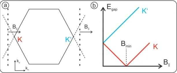
As mentioned already above in the zone-folding approximation a carbon nan- otube is metallic if the one-dimensional sub-bands intersect one of the K or K 0 points located at (k x a, k y a) = 0, ± 4π 3 . Using equation 2.8 a carbon nanotube intersects the valleys for
0 · (m + n) ± 4π 3 · 1
2 (m − n) = 2πq. (2.10) Since q is an integer, this is fulfilled for (n − m) = 3q. Thus, every third carbon nanotube would be expected to show metallic behavior.
Armchair type
Armchair carbon nanotubes are rolled up in ~ x-direction; so ~k x corresponds to ~k ⊥
and ~k y corresponds to ~k k . The quantization of ~k ⊥ is given by
2.2. Carbon nanotube band structure 10
√ 3nak ⊥ = 2πq. (2.11)
Accordingly one obtains a spacing of the sub-bands in ~k ⊥ -direction as
k ⊥ = 2πq
√ 3na . (2.12)
This situation is sketched in figure 2.2(b). One can see that the sub-band for q = 0 will always intersect the points (k x a, k y a) = 0, ± 4π 3 ; so armchair carbon nanotubes are always metallic.
Using the dispersion relation of graphene the resulting one-dimensional dispersion relation in ~k y -direction for an armchair carbon nanotube reads
E(k x , k y ) = ±
(
1 + 4 cos
πq n
cos k y a 2
!
+ 4 cos 2 k y a 2
!) 1/2
. (2.13) In figure 2.3(a) and (b) the band structure of a (2,2) carbon nanotube and of a (7,7) carbon nanotube are depicted; no band gap exists and the carbon nanotube has metallic behavior like expected for armchair carbon nanotubes.
Zigzag type
In a zigzag type carbon nanotube the quantization is given by
nak ⊥ = 2πq ⇒ k ⊥ = 2πq
na (2.14)
and the band structure reads as
E(k x , k y ) = ±
(
1 + 4 cos
√ 3k x a 2
!
cos
πq n
+ 4 cos 2
πq n
) 1/2
. (2.15)
Figure 2.3(c) shows an exemplary (5,0) zig-zag carbon nanotube; as mentioned
above a (5,0) zigzag carbon nanotube has a band gap since (n − m) = 5 6= 3q
for an integer q. This can also be seen in the calculated band structure using
equation 2.15; a band gap arises. In figure 2.3(d) the band structure of a (6,0)
zig-zag carbon nanotube is depicted also using equation 2.15. Now the condition
(n − m) = 6 = 3q is fulfilled for q = 2, the carbon nanotube is metallic, and no
band gap exists.
3 2 1 1 2
3 2 1 1 2 3
k a
yE
k a
yE
3 2 1 1 2
3 2 1 1 2 3
(2,2) (7,7)
a b
c d
k a
xE
3 2 1 1 2
3 2 1 1 2 3
k a
xE
3 2 1 1 2
3 2 1 1 2 3