Validation Method for Array Processor in Space Validierungsmethode für einen Array Prozessor in der Raumfahrt
Masterarbeit
im Rahmen des Studiengangs Informatik
der Universität zu Lübeck vorgelegt von
Sven Ott
ausgegeben und betreut von Prof. Dr. Martin Leucker
Die Arbeit ist im Rahmen einer Tätigkeit bei der Firma Airbus DS GmbH entstanden.
Lübeck, den 15. April 2016
Abstract
The High Performance Data Processor (HPDP) is a novel processor architecture for stream-based data processing applications in space systems. It combines a coarse-grained reconfigurable dataflow array, sequential processing units, and space-oriented periph- erals. Flexibility and an in-orbit programmable core provide a full range of processing capabilities for a long operational lifetime.
This work analyses the current development state of the HPDP chip, followed by estab- lishing a suitable on-board test method for commissioning. In particular, the test concept covers critical internal components, memories, as well as interfaces at the processor’s op- erational speed using the instruction set. The correctness of the developed test programs is demonstrated in ModelSim using an accurate design of the HPDP.
Zusammenfassung
Der High Performance Data Processor (HPDP) basiert auf einer neuen Prozessortechno- logie für Stream-basierte Datenverarbeitungsprogramme in der Raumfahrt. Es vereint ein konfigurierbares Datenfluss-Array, sequenzielle CPUs und raumfahrttaugliche Schnitt- stellen. Eine breite Anwendung und lange Einsatzzeit sind durch die flexible Program- mierung während einer Mission gewährleistet.
Die vorliegende Arbeit analysiert den aktuellen Entwicklungsstatus des HPDPs und stellt darauf aufbauend eine geeignete Testmethode für die Inbetriebnahme vor. Das verwende- te Konzept beinhaltet das Testen von kritischen internen Komponenten, Speichermodulen und Chip-Schnittstellen unter der operativen Geschwindigkeit des Prozessors. Die ent- wickelten Testprogramme wurden in ModelSim mit einem vollständigen HPDP Design simuliert.
Erklärung
Ich versichere an Eides statt, die vorliegende Arbeit selbstständig und nur unter Be- nutzung der angegebenen Hilfsmittel angefertigt zu haben.
Lübeck, 15. April 2016
Acknowledgements
I would like to give special thanks to Tim Helfers for giving me the opportunity to write this thesis at Airbus Defence and Space and the guidance throughout the period.
Thanks to Prof. Dr. Martin Leucker from the Institute for Software Engineering and Programming at the University of Lübeck for supporting my work at the other end of Germany.
Big thanks to Daniel Bretz and Volker Baumgarte for their great help to understand the HPDP architecture quickly and work more efficient with the different simulations tools.
Also, great thanks to my friends Jonathan Felix and Kevin Böckler for their advice to make this thesis even better.
Contents
1 Introduction 1
1.1 Purpose of the Thesis . . . 2
1.2 Structure of the Thesis . . . 2
1.3 Software used throughout this Thesis . . . 3
2 High Performance Data Processor (HPDP) architecture 5 2.1 Top Level Design . . . 5
2.2 XPP-Core . . . 6
2.2.1 XPP Dataflow Array . . . 7
2.2.2 FNC-PAE . . . 9
2.2.3 Memory Access . . . 9
2.2.4 Other components . . . 10
2.3 Periphery . . . 11
2.3.1 SpaceWire . . . 11
2.3.2 Stream-IO Block . . . 11
2.3.3 Memory Ports . . . 12
2.3.4 Watchdog . . . 12
2.3.5 GPIO . . . 13
2.3.6 System Controller . . . 13
3 Design analysis 15 3.1 Previous design verification . . . 15
3.1.1 Verification by PACT . . . 15
3.1.2 Verification of complete HPDP design . . . 16
3.1.3 Manufacturing tests . . . 17
3.2 Discussion . . . 17
3.2.1 Drawbacks of software simulations . . . 18
3.2.2 Testing HPDP interfaces . . . 19
3.2.3 Accessibility of memory modules . . . 19
3.2.4 Clock-domain crossings and power supply . . . 20
3.2.5 XPP Array test . . . 21
3.2.6 Components tests . . . 21
Contents
4 Test concept 23
4.1 Test approaches in Processor Testing . . . 23
4.1.1 External tester . . . 23
4.1.2 Built-in self-test (BIST) . . . 24
4.1.3 Embedded software-based self-testing (SBST) . . . 24
4.1.4 Previous Work for SBST . . . 25
4.2 Test setup . . . 27
4.2.1 Board Level Test System (BLTS) . . . 27
4.2.2 Single-chip Board . . . 28
4.2.3 Multi-chip Board (HPPM) . . . 28
4.3 Test strategy . . . 29
4.3.1 Source and sink pattern . . . 29
4.3.2 Procedure of a single test program . . . 30
4.3.3 Sequence of several programs . . . 31
4.3.4 Memory testing . . . 32
4.4 Test phases . . . 33
4.4.1 Basic-functional tests . . . 33
4.4.2 Functional integration tests . . . 34
4.4.3 Summarizing . . . 37
5 Implementation 39 5.1 Tools and target platform . . . 39
5.1.1 xsim . . . 39
5.1.2 ModelSim . . . 40
5.1.3 Single-chip board and the HPDP chip . . . 41
5.2 Test flow realization . . . 43
5.2.1 Configuration phase . . . 44
5.2.2 Program copy . . . 44
5.2.3 Keep the duration optional . . . 46
5.2.4 Waiting for response . . . 46
5.3 Test case implementation . . . 48
5.3.1 Memory connectivity testing . . . 48
5.3.2 XPP Array . . . 50
5.3.3 Interfaces . . . 50
5.3.4 Watchdog timer . . . 50
5.3.5 Stressing the entire HPDP chip . . . 51
5.4 Multi-chip board (HPPM) testing . . . 52
x
Contents
6 Evaluation 55
6.1 Verification . . . 55
6.1.1 Inserting faults via SpaceWire . . . 55
6.1.2 Using faulty C-routines . . . 56
6.1.3 Forcing signals motivated by Mutation testing . . . 56
6.1.4 Final realisation . . . 57
6.2 Results . . . 57
6.2.1 Runtimes . . . 57
6.2.2 Integration of further algorithms . . . 58
6.2.3 Arisen problems . . . 59
7 Conclusion 61 7.1 Conclusion . . . 61
7.1.1 Extensibility . . . 61
7.1.2 Using ModelSim . . . 61
7.2 Open questions . . . 62
A Appendix 63 A.1 Technical data . . . 63
A.2 Code example . . . 64
A.3 Test cases . . . 66
1 Introduction
The demand for high-performance earth observation satellites is significantly growing.
New sensor technologies with increasing resolutions and rising instrumental data rates require a cost-effective, real-time performance of on-board data management and high- speed downlink to earth. A high-performance data processor is required, which can handle the rising amount of data, and further, can lower costs of other on-board equip- ment by reducing downlink data. Moreover, new transmission formats and standards demand in-space reconfigurability to avoid a limitation of satellite’s functionality for its whole life. [SHW+08]
A suitable hardware architecture must support pipelining and data flow parallelism on the one hand, and on the other, offer an in-orbit programming flexibility for the processing components. Application-Specific Integrated Circuits (ASIC) is an advanced architecture providing high operating performance while energy consumption is low. Flexibility might be reached by implementing multiple functionalities on a single or multiple con- nected chips. However, the lack of reconfiguration capabilities is an inevitable drawback of ASICs. A more flexible architecture are Field Programmable Gate Arrays (FPGA) based on SRAM, offering reconfiguration at the gate level, but they need more space and a higher power consumption at less operational frequency than an ASIC. Also, there are some con- cerns about radiation effects, and internal data can not be stored during reconfiguration.
Another approach solving the arising problems might be a digital signal processor (DSP).
Its architecture is specialised for data-processing applications, and the algorithms are coded in software. While a high flexibility and in-orbit reconfiguration is given, high power consumption is disadvantageous. Moreover, the computational performance for stream-based applications is not as high as FPGAs or ASICs. [BEM+03, SHW+08]
A new emerging technology is an array processor that combines the benefits of other established architectures. A high computational performance with low power consump- tion, while being reprogrammable at any time, makes that processor class a promising technology for the earth observation field. The eXtream Processing Platform (XPP) archi- tecture is based on such a reprogrammable array processor technology and forms the core of the High Performance Data Processor (HPDP), that is used throughout this work. The flexible and reliable architecture can process a high amount of data concurrently and is re-
1 Introduction
programmable at runtime. Pipeline, instruction level, data flow, and task level parallelism fulfil the requirements of heterogeneous applications in fields such as telecommunication, simulation, digital signal processing, and cryptography [PAC09g, SAH13].
Moreover, a new radiation-hard, 65-nm semiconductor technology is used for manufac- turing the HPDP chip. This technology is not space-proven yet.
The HPDP comprises various complex and heterogeneous components those are ar- ranged on a single chip. A whole set of testing challenges has arisen through the long development process. Signal integrity (SI) must be preserved in digital circuits as such problems can cause a failure to operate at the planned operational speed, that makes the circuit unreliable. Known causes are crosstalks, ringing, ground bounce or noise in the power supply. Those may lead to wrong or delayed signals, or reduce the lifetime of processor chip due to additional hardware stress.
1.1 Purpose of the Thesis
The goal of this work is to develop a test strategy bringing the new HPDP chip with its new semiconductor technology into operation. A commissioning test plan shall be estab- lished along with the on-board test software to verify the reliability of internal features and interfaces of the new array processor technology. Meanwhile, the first HPDP demon- strator chip is in the manufacturing phase and, therefore, not provided throughout this thesis. Suitable verifications are required to ensure the reliability of developed commis- sioning tests. Simple usability and good extensibility are essential because later the test method will be used by an HPDP chip reviewer.
The processor utilises a new manufacturing process of a 65-nm radiation-hard technology which also must show its reliability in practice. However, testing of the physical persis- tence under extreme conditions in space is not part of this thesis. Whereas, stress tests under normal circumstances shall be included.
1.2 Structure of the Thesis
The first section introduces the HPDP architecture from its top level design down to the module level. The subsequent section analysis the verification process of the HPDP de- sign and shows which test will be applied in manufacturing. After that, a discussion about additional tests for commissioning is given. The fourth section starts with an introduction of different approaches in hardware testing along with a short review of the literature.
After introducing the test setup, the detailed concept including test flow and individual test cases is described. Next, the implementation section explains the realized of on-board
2
1.3 Software used throughout this Thesis tests into detail. Afterwards, the next section shows how the commissioning tests are ver- ified, and presents the results. Finally, a conclusion summarizes the work and addresses open issues.
1.3 Software used throughout this Thesis
The commissioning method is implemented using two different development kids. First, the PACT XPP SDK provides several tools for compiling, simulating, visualizing, and debugging source code for the XPP-Core of the new array processor. Second, a ModelSim testbench provides a more detailed and comprehensive simulation model of the HPDP design.
2 High Performance Data Processor (HPDP) architecture
The target applications of the High Performance Data Processor (HPDP) are for high data volumes in the signal-processing domain. The flexible and in-orbit reconfigurable core is fully programmable and provides a full range of processing capabilities. The HPDP includes the eXtreme Processing Platform (XPP) Intellectual Property (IP) from PACT that combines a coarse-grained reconfigurable dataflow array with sequential processing units. Additional, space-oriented modules such as data transfer and memory interfaces are added by Astrium. [PAC09a]
The final semiconductor technology for the HPDP is 65 nm wide and radiation-hardened.
The planned operational clock frequency is 250 MHz due to the space conditions. This chapter gives an overview of the processor design and its functionality from the top level design down to the module layer.
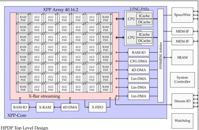
2.1 Top Level Design
The HPDP chip comprises the XPP IP core along with useful peripherals. The XPP-Core is based on the 40.16.2 XPP Dataflow Array and two Functional Processor Array Units (FNC-PAE), surrounded by different memory access and streaming objects, as well as a packet-oriented communication network. [PAC09h]
The high-speed interfaces SpaceWire with three links and the Stream-IO block with four channels offer access for controlling and data transfer with other board elements such as additional HPDP chips or instruments. The System Controller manages the different clock frequencies of the chip and peripherals. It also has a JTAG (Joint Test Action Group) interface and different operation modes for testing and debug purposes. The XPP Memory Arbiter provides interfaces for three memory ports. The first port can connect the chip to an EEPROM or SRAM, mainly to store instruction code. The second port is suitable for a large SRAM or SDRAM storage, and the third interface already connects an internal 4 Mbyte SRAM. Further, a watchdog module observes a program execution and throws an interrupt if a program does not reset the watchdog timer in a chosen period. [SH10] The Top Level Design is represented in figure 2.1, where the blue area shows the XPP part that is explained in more detail in section 2.2. The following section describes the peripheral components represented in the white area of figure 2.1.
2 High Performance Data Processor (HPDP) architecture
XPP-Core
HPDP Top Level Design
RAM PAE RAM PAE RAM PAE RAM PAE RAM PAE RAM PAE RAM PAE RAM PAE
ALU PAE ALU PAE ALU PAE ALU PAE ALU PAE ALU PAE ALU PAE ALU PAE
ALU PAE ALU PAE ALU PAE ALU PAE ALU PAE ALU PAE ALU PAE ALU PAE
ALU PAE ALU PAE ALU PAE ALU PAE ALU PAE ALU PAE ALU PAE ALU PAE
ALU PAE ALU PAE ALU PAE ALU PAE ALU PAE ALU PAE ALU PAE ALU PAE
ALU PAE ALU PAE ALU PAE ALU PAE ALU PAE ALU PAE ALU PAE ALU PAE
RAM PAE RAM PAE RAM PAE RAM PAE RAM PAE RAM PAE RAM PAE RAM PAE
X-Bar streaming
XPP Array 40.16.2
CPU ICache DCache
CPU ICache DCache 2 FNC-PAEs
RAM-IO CFG-DMA
4D-DMA Lin-DMA Lin-DMA Lin-DMA
RAM-IO X-RAM 4D-DMA X-FIFO
SpaceWire
MEM-IF MEM-IF
SRAM
System Controller
Stream-IO
Watchdog
SYSMEMArbiter
Figure 2.1: Overview of the HPDP architecture; the blue area contains the XPP-Core, the white part additional pheripherals; the arrows show the directions of data and event flow
2.2 XPP-Core
The integrated XPP-Core comprises the XPP Array, two FNCs, storage components, vari- ous memory access modules, as well as a communication network with point to point or point to multi-point connections. The dataflow array consists of two different Processor Array Elements, ALU-PAEs and RAM-PAEs, and runtime-configurable communication buses. The operational fields are high-bandwidth stream-based applications. Two FNC- PAE are coupled to the array’s communication channels and perform high-performance execution of irregular and control-dominated algorithms. They are also in charge of the system management, i.e., control DMA operation. Various DMA controllers transfer data between external memories and the XPP components. Integrated FIFOs uncouple the DMA channels from the system memory bursts and potentially stalled pipelines within the XPP core. At runtime, configurable X-Bar switches connect the streaming input and output ports of on-chip components. The SYSMEM-Arbiter handles concurrent RAM ac-
6
2.2 XPP-Core cesses of various memory channels from the XPP side to the three memory ports, or vice versa. [PAC]
2.2.1 XPP Dataflow Array
The dataflow array has about 150 16 bit-wide ALUs and 16 small 512 Mbyte SRAMs and is fully reprogrammable by the Config-DMA. Vertical routing registers and horizontal rout- ing buses connect the components via 16-bit data and 1-bit event connections. I/O objects on the left and right sides offer functionality for the link with other XPP components via crossbars. Thereby, a ready/acknowledge protocol for communication is employed guar- anteeing self-synchronization. [PAC09g]
Each array unit performs its programmed operation as soon as all required data or event input packets are available. Afterwards, the ALU forwards the result once it is computed.
Hardware protocols handle pipeline stalls automatically. During a clock cycle, an XPP Dataflow object consumes data and event packets from its input ports, performs the con- figured operation and releases the result on the output ports if the previous packet has been consumed. If not all required input ports for the set operation are covered by a packet, the computation unit does not perform any action. Further, there are two different Processor Array Elements: Arithmetic Logic Unit PAEs (ALU-PAE) and Random Access Memory PAEs with I/O (RAM-PAE with I/O). [PAC09h]
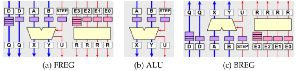
ALU-PAE
An ALU-PAE, shown in figure 2.2, consists of three different objects that can execute a separate opcode from a limited list of operations. The ALU-object is located in the mid- dle and performs arithmetical and boolean operations, as well as comparisons. The For- ward Register-object (FREG) and Backward Register-object (BREG) offer operations for flow control, data manipulation, counters and shift operations, and are in charge of ver- tical routing. Additionally, FREG and BREG objects have two input FIFOs with one and four stages each to support pipeline balancing. During the configuration phase, preload- ing of values into FIFOs is possible. The output registers can store one value to guarantee that pipeline stalls do not lead to packet loss. [PAC09g]
RAM-PAE
The left- and the rightmost column of the Data-flow Array consists of RAM-PAE objects.
Those have one internal RAM object, one I/O object, and also an FREG and BREG object for vertical routing. The I/O object provides the ability for direct communication of the Array with other XPP components such as the FNCs or memory access objects. Both
2 High Performance Data Processor (HPDP) architecture
(a) FREG (b) ALU (c) BREG
Figure 2.2: The three objects of an ALU PAE: Forward Register-, ALU- and Backward reg- ister objects with input FIFOs and funtional units (red: event channels, blue:
data channels)[PAC09g]
(a) IO (b) RAM
Figure 2.3: The objects of an RAM PAE: I/O-object with streaming ports and input FIFOs, RAM-object with interal memory and input FIFOs[PAC09g]
data and events can be transferred between the ports of an I/O object and the connected network ports.
The internal RAM object works as a cache for the other array elements. It is not directly accessible from the outside but can be filled with arbitrary values at configuration time.
Each RAM object can store up to 512 Mbytes and a RAM mode as well as a FIFO mode are available. Figure 2.3 depicts the RAM-PAE object. [PAC09g]
Bus Switch Object
The XPP Array includes unidirectional data and event buses for horizontal routing. Bus switches have a delay of one register and also includes one FIFO stage in their input ports.
[PAC09h]
Data and Event Streams
In the XPP architecture, single data and event packets travel through the flow graph se- quentially. Thereby, 1-bit events may be used for synchronizing external devices.
All array components work with self-synchronization which means that an output packet is only generated when all required input data and event packets are available. That simplifies programming and compiling of dataflow-oriented algorithms because only the
8
2.2 XPP-Core
Figure 2.4: A FNC-PAE includes eight ALUs arranged in two colums, a Special Functional Unit (SFU), 16 bit registers, 32-bit address generator (AG) and a L1 Instruction cache and data cache [PAC09g]
number and order of packets travelling through a graph representation is important rather than the timing of the pipeline. [PAC09g]
2.2.2 FNC-PAE
The HPDP architecture has two Function Processing Array Elements (FNC-PAE) that are sequential 16-bits Harvard architecture processors and comprises a design similar to the Very Long Instruction Word (VLIW). The differences are an implicit conditional operation and sequential and parallel execution of eight ALUs in one clock cycle. Four ALU ele- ments are arranged in one data path so that four ALUs can be chained. Also, predicted execution can be implemented. [PAC09a]
Therefore, an FNC-PAE is specialised for typical signal processing algorithms and for housekeeping tasks such as programming DMA components or reconfiguring the XPP Array. An FNC-ELF-GCC compiler provides the ability to execute legacy C-code. Each FNC-PAE includes L1 data and instruction cache, whereby the L1 D-cache can be used as tightly-coupled memory (TCM) alternatively. Further, a Special Functional Unit (SFU) for executing instructions like multiplication is available. [PAC09g]
2.2.3 Memory Access
Three different direct memory access (DMA) types can transfer data streams between XPP components and the System Memory Arbiter (SYSMEM Arbiter) that forwards the data to the different memory ports.
2 High Performance Data Processor (HPDP) architecture
SYSMEM Arbiter
The System Arbiter processes all memory read and write requests from XPP Core compo- nents such as FNC-PAE, Linear DMA, and 4D-DMA to the corresponding memory out- puts. The arbiter routes the requests independently, is fully pipelined and supports burst memory access and programmable prioritization. [PAC09h]
Linear DMA
The HPDP has three Linear DMA controllers that provide data stream accesses from the core to the memories connected to SYSMEM Arbiter, or vice versa. It automatically gen- erates linear increasing addresses from a given address range and converts a 16-bit input stream into 64 bit-wide sequence for write access. Likewise, a memory read access is transformed into an output stream. [PAC09h]
4D-DMA
If a more complex, multi-dimensional address pattern is required, the 4D-DMA controller can be used to generate 4-dimensional address patterns. The HPDP owns four indepen- dent 4D-DMA modules for read and write access. Each 4D-DMA operates in one direction and has various modes from single 16-bit streaming until using the full 64-bit of a memory channel. [PAC09g]
RAM-IO
The RAM-IO object is a custom-built model that provides arbitrary access pattern for un- restricted 32-bit memory access between the XPP Array and external RAMs because a Dataflow Array element can only deal with 16 bit. Three data ports and one event port are available, and integrated FIFOs and buffers provide fully pipelined access to memo- ries. [PAC09b]
2.2.4 Other components X-RAM
The X-RAM is a small local buffer memory that is only accessible from the dataflow array via write 4D-DMA-L0 controller or the RAMIO-L object. It provides 8192 words of 16 bit each. [PAC09g]
10
2.3 Periphery
X-FIFO
The X-FIFO module can be used as a buffer for any XPP 16-bit data stream. It uncouples a data source from a target of a stream-based processing chain, for example, to avoid stalling in data exchange between an FNC-PAE and the XPP-Array. [PAC09c]
X-Bars - Network on Chip
The XPP communication includes data streams, event streams and memory streams. The X-Bar components build the routing network on the XPP-Core and routes data or events from one input to one or more outputs. The data flow is automatically synchronized, and up to four packets can be stored if the pipeline stalls. Therefore, a component consumes a packet only if all required input packets are available, and the result is only forwarded if the previous results have been consumed. The transmitting system transfers one packet by cycle, and no packets can get lost during a pipeline stall or re-configurations process.
[PAC09e]
2.3 Periphery
The Periphery extends the XPP IP core with interfaces for communication, data transfer and external memories to customize the array processor for the target area in space appli- cations.
2.3.1 SpaceWire
The standardized SpaceWire is a spacecraft communication network specified by ESA (Eu- ropean Space Agency). It is used for controlling and monitoring the HPDP chip, as well as loading new configurations or programs into RAM. The SpaceWire module consists of three links and implements RMAP (Remote Memory Access Protocol) for path address routing and limited logical address routing from one SpaceWire link to another. That rout- ing capability allows a large number of HPDP chips to interface with a single SpaceWire port on the command & control module. After chip reset, all three links are in autostart mode so that a start configuration for activating a link is not necessary. The target data rate of the packet transport is 200 Mbits/s. [Lem10]
2.3.2 Stream-IO Block
The Stream-IO module of the HPDP chip is a 16-bit wide, point-to-point bidirectional data stream interface. It provides four high-speed data communication channel links with
2 High Performance Data Processor (HPDP) architecture
start idle
wdog = 0
wdog started
wdog bark
wdog interrupt = 1 wdog vector6=0
wdog restart = 1
wdog > wdog vector wdog tick = 1
wdog++
wdog reset = 1
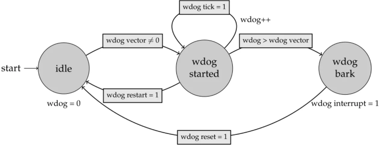
Figure 2.5: The state machine of the watchdog module
external devices, such as other HPDP chips or FPGAs, or on-board instruments. Addi- tionally, a simple hardware protocol provides full handshake control, and different clock domains for both communication sides are possible. [PAC09d]
2.3.3 Memory Ports
The HPDP architecture includes three memory ports. All interfaces are connected with the SYSMEM Arbiter that provides a 64-bit memory channel interface. All external memories provide an EDAC (Error Detection and Correction) based on Hamming Code for protec- tion against radiation effect. Port 0 is used as configuration memory and can be connected to a PROM/EEPROM or SRAM device storing boot code or application code. Its address space is divided into two parts. The lower address space belongs to the external mem- ory interface, and the higher one targets the AHB master bridge to control various HPDP registers such as SpaceWire or Watchdog. Therefore, it is possible to send data from mem- ory port 0 to external devices via SpaceWire. Memory port 1 can link either an SRAM or SDRAM memory. Port 2 is already connected to an integrates 4-Mbyte SRAM module.
[Lem10] Appendix A.1 contains a tabulated overview of the connected memories (table A.1) and other technical data of the HPDP chip.
2.3.4 Watchdog
A watchdog is a necessary module for fault detection in space equipment. It is used to detect failures that affect cyclic program execution by the HPDP. Whenever the time elapses, an interrupt is set to detect the error by the controller [Skl76].
12
2.3 Periphery Figure 2.5 depicts the state machine of the watchdog module. If the wdog vector is unequal zero, the watchdog automatically starts and increases the value of wdog at every clock cycle by 1. When the value is higher than the programmed vector, the state machine switches to the wdog bark state where an interrupt is triggered. Afterwards, the wdog resets by itself. The wdog vector is divided into two registers, a prescaler and a value, to provide 32-bits since 16 bits would not be enough [Lem10]
2.3.5 GPIO
The GPIO (General-purpose input/output) provides eight pins for input and output sig- nals those can be written or read by the FNC-IO-BUS. The GPIO should be used for simple input and output signals under FNC-PAE software control. Particularly, an input signal can be used to read configuration switches or to capture the status of external devices. An output pin is useful to steer debug LEDs or control external devices. [PAC08]
2.3.6 System Controller
The HPDP System Controller includes several PLLs (Phase-locked loop) that are respon- sible for the input clock generation of the XPP array, FNC-PAEs, SpaceWire, memory con- troller, and Steam-IO. All clocks are synchronous and can be adjusted by a divider and multiplier. Furthermore, the System Controller contains a debug controller and JTAG in- terface. [Bau15]
3 Design analysis
The HPDP development started around ten years ago. Several design verification meth- ods and techniques have been applied on the functional level and hardware level. This chapter analyses what has been done, followed by a discussion of what additional tests should be done to bring the new array processor technology into operation.
3.1 Previous design verification
The complex System-on-Chip (SoC) design consists of an enormous number of modules, different bus systems, and memories. Thereby, two design methodologies characterise the chip due to historical reasons. That follows a proper verification strategy is needed to guarantee the correct function of the HPDP chip [LS10].
The following subsections give an overview of tests performed on the HPDP chip. The outline based on the documents [LS10] and [PAC09f].
3.1.1 Verification by PACT
The XPP-III IP core of the HPDP chip was developed by PACT, which has created inte- grated test suites and test benches during the design process. That includes functionality as well as top-level design tests. Moreover, all XPP-III components are co-designed in Verilog and System-C. A Design Checker reviews the Verilog code. The test benches are self-checking and can be used for RTL and gate level simulations.
Besides small component tests, application tests have shown that the processor archi- tecture is capable of executing relevant applications using the full ability of XPP core.
Examples are a JPEG encoder, FIR filter or Fast Fourier transform.
The FNC-PAE is the most complex module of the HPDP architecture. Therefore, own sample applications have been created. Both an FNC Software Simulatorxfncsimas well as an RTL simulator for the Verilog specification, execute test cases to prove functional correctness. These two test frameworks generate the same kind of trace files that con- tain detailed information about the internal state of an FNC-PAE in every clock cycle.
These trace files are useful to prove the equality of both test results since the Verilog and SystemC code are based on the same HPDP specification. Besides, line coverage of the Verilog code is analysed using hardware development tools.
3 Design analysis
However, the simulators have a different cycle accuracy due to the complexity of some modules like L1-caches or hardware dependencies. The simulation language SystemC is not able to simulate an asynchronous clock domain that is located between the FNC- Container and the system memory arbiter. The simulation uses a simplified model that mocks a corresponding number of cycles for a cross-domain simulation.
An additional SystemC simulation tests the XPP Array and the interacting modules for networking and direct memory access on the system level. The same trace file strategy as for the FNCs is used.
Further, simple and complex access patterns verify the memory interfaces. The Stream-IO block is also provided by PACT in an extra module with an own test suite because it is not part of the actual XPP IP core.
3.1.2 Verification of complete HPDP design
The final version of HPDP combines the PACT modules XPP-III 40.16.2 core and Stream- IO block, and supplemental modules such as a SpaceWire module, three memory ports, a System Controller, and a JTAG Controller.
Verification tests consist of several steps that are performed on a module, a sub-system and at top-level. Those tests ensure that the HPDP chip is operating correctly, according to its specification.
In the first step, the complete integration of Astrium-modules is verified at the design and subsystem levels. Besides, test cases check interconnections and module overlapping functionalities such as interrupts, read and write on memories and registers.
The second step contains integration of the PACT testbench in the Astrium developed test benches to simplify the integration of Astrium modules into PACT-IP.System level functionalities, top-level modules, and pad interconnections are tested.
To achieve a sufficient design coverage, test generation application (TGA) generate a cou- ple of tests automatically. Several of those TGAs are contained in the verification en- vironment and create multiple tests to cover different fault classes of a certain feature.
Moreover, single XPP components are tested with an extensive regression regression test suite.
Included application tests have been written to nearly cover all modules of the top-level design. Several component tests use connectivity modules of the top-level design such as crossbars and memory arbiters in passing. Therefore, those components are also assumed to be fault-free.
16
3.2 Discussion Two memory ports connect an external data carrier with the HPDP chip. Those memory blocks come from external providers, and it may assume that those are well tested.
Hardware must resist certain physical conditions. Primarily space equipment is exposed to high and very low temperatures during operation and idle state. The maximal power consumption and the consequent cooling demand can be calculated with tools, and the chip vendor will guarantee the estimated thresholds.
3.1.3 Manufacturing tests
Two steps of equivalence checking will be done during the implementation process. First, Astrium proved the equivalence between the RTL code and the netlist transferred to the Backend Design house using formal verification techniques. Second, equivalence checks between the transferred and the final produced netlist will be performed before delivery.
These controls shall guarantee a proper functionality of final hardware relation to design.
The HPDP netlist is designed by using the design for testability (DFT) technique which means that testing features are added to the chip simplifying developing and applying manufacturing tests to the designed hardware. Therefore, the processor contains scan- chains, boundary scans, and two additional debug modes next to the regular operation mode. That offers the option to observe and test every flip-flop in debug mode, included read and write to internal RAMs or FNC instructions.
A BIST (Built-in self-test) logic and the corresponding BIST mode verify the correctness of each internal RAM cell by applying different test patterns created by an ATPG (Automatic Test Pattern Generator). [Lie10]
Further, static timing analysis (STA) will be done following the rules from the chip vendor.
It contains best and worst case analysis in typical modes. STA is capable of checking every structural path and can detect glitches, slow parts and clock skews using scan shifts, stuck- at capture and delay capture. Power Distribution, Voltage (IR) Drop and Electro-migration on chip shall be tested, as well as observation of the PLL performance. [Bau15]
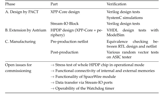
3.2 Discussion
The HPDP chip is based on a new technology of array processors that is not well es- tablished yet. Therefore, carefully testing of the semiconductor could be necessary after manufacturing. As the previous section has shown, many tests are already done before commissioning. The design is thoroughly verified using various tools and testbenches;
the circuit is designed for testability (DFT) and post-production tests as boundary scans and delay tests will be applied. Consequently, the assumption is that the manufactured
3 Design analysis
Phase Part Verification
A. Design by PACT XPP-Core design Verilog design tests SystemC simulations Stream-IO Block Verilog design tests B. Extension by Astrium HPDP design (XPP-Core + pe-
riphery)
VHDL design tests with ModelSim
C. Manufacturing Pre-production netlist Equivalence checking be- tween RTL design and netlist Post-production Various random vector tests
on ASIC tester
Open issues for →Stress test of whole HPDP chip in operational mode commissioning →Functional connectivity of internal and external memories
→Functionality of SpaceWire module
→Data transfer via Stream-IO ports
→Operability of the Watchdog timer
Table 3.1: An overview about the different design phases and open issues. Each phase is divided into the central parts and tests those are done or are going to happen before delivery.
chip comprises the expected design and should be free of hardware faults.
However, additional tests on the fabricated HPDP chip are required to ensure the compli- ance of realised technology, because the simulations cannot fully guarantee the intended hardware behaviour of the manufactured semiconductor, and the manufacturing tests do not run software programs. Thus, the regular interaction of written software and the designed HPDP architecture must still be demonstrated on real hardware. The next subsections analyse and discuss the available software tools for developing, as well as internal features and interfaces those are interesting for commissioning tests. Table 3.1 gives an overview of the analysis.
3.2.1 Drawbacks of software simulations
Various SystemC simulations and a given ModelSim testbenches can simulate the complex HPDP design and prove its correctness. However, those have different disadvantages regarding the limited scope and simulation time.
Due to the nature of the system-level of SystemC tools, the simulations for the XPP core
18
3.2 Discussion or only the FNC-PAE are quite fast and can simulate millions of clock cycles in a reason- able amount of time. Some modules, like the SpaceWire, have been added later and are not included, which limits the SystemC simulations and makes it impossible to develop a whole commissioning test suite. Also, the system-level simulations simplify the steps for computing but prevent the simulation of correct timing. In particular, the timing of Clock Domain Crossings, FNC caches, and external memories are not represented cor- rectly [LS10].
The ModelSim tool follows a different approach simulating Verilog or VHDL code at the register-transfer (RT) level. Consequently, the simulation is very close to the real hard- ware and details are much better represented than a SystemC simulation does. However, the enormous complexity of the HPDP design makes an RT-level simulation very costly in runtime and required memory. Hence, a simulation time of a few milliseconds can take several hours. Although all components of the final HPDP chip are present in the Model- Sim testbench, testing of complex algorithms is very time-consuming for fast prototyping of commissioning tests.
As an example, it is acceptable to verify the watchdog with a small timer so that the watch- dog interrupt is triggered after a short simulation time. When the timer, however, adds up to a couple of seconds to trigger, in the case of testing also high values, it would take days of simulation only for one test. Of course, the design is standardised, and if the logic works for milliseconds with a complete code coverage, it should also work for seconds or minutes. However, the hardware is complex and must also be proven if that is the case.
Besides, the watchdog timer is a peripheral module and is not included in the XPP-Core.
3.2.2 Testing HPDP interfaces
Using the HPDP chip requires a board that provides ports and slots for SpaceWire, Chan- nel links (Stream-IO), GPIO, and memories. As the planned board and processor chip are manufactured independently, the connections between the board and chip are not verified before commissioning.
Thus, an important part of the commissioning testing is the verification of the reliability of all interfaces. Chapter 4 introduces the test setup and describes the available interfaces in detail.
3.2.3 Accessibility of memory modules
The planned board provides two board memories which utilise the HPDP for data and program storage. Further, the processor chip contains several internal RAMs and caches.
With the design for testability (DFT), each memory has a Built-in-Self-Test (BIST) that is
3 Design analysis
an approved standard and checks every memory cell with different addresses and value patterns. Moreover, external memories can be assumed to be well tested by suppliers.
However, the functional accessibility of each memory by the computation units remains an open question. Data processing validation must show that each memory is probably connected and addressable by functional units or the SYSMEM arbiter. For this, a test may apply different input vectors such as all-zero pattern, all-one-pattern, random, or counter pattern. Further, L1 data cache and instruction cache of FNC-PAEs can not be directly addressed by C-Code or Assembler (only a half of L1-D-Cache is usable as Tightly Coupled Memory (TCM) [PAC]. Hence, FNC stress tests are also required to reach a good test coverage of FNC memories.
3.2.4 Clock-domain crossings and power supply
The HPDP is expected to have an operational speed of 250 MHz. That clock frequency ap- plies to the central part of the XPP-Core, which includes the XPP-Array and the memory access components. The FNC-container, in turn, runs on a unique clock domain, which has half of the XPP-Core’s operational speed, i.e. 125 MHz. All data transfer modules need to deal with the frequency of the channel connected to the HPDP. Therefore, clock-domain crossings are included whenever two clock domain meet. There are also several clock do- mains inside the chip, since planned clock frequencies for external memories, SpaceWire and Stream-IO may less than the HPDP reference clock. Delay faults make those clock- domain crossings vulnerable to metastability, data loss, and data incoherency. Although the manufacturing tests should be quite comprehensive, their effectiveness under opera- tional conditions is questionable [KCGP12].
For that reason, stress tests are suitable to determine the stability of clock-domain cross- ings and power distributions under operational conditions. The higher the processor fre- quency, the more vulnerable the hardware is for such defects [CDS+00]. That implies that component tests should also be done on a real HPDP to guarantee a correct behaviour of internal features and interfaces under full load.
A software program is suitable for stress testing since instructions utilise the entire chip rather than only a few units. Consequently, comprehensive stress tests should be done running with a maximum number of functions and interfaces to discover potential side- effects on the power supply and establish the proper integration of critical components.
[KLC+02]
20
3.2 Discussion
3.2.5 XPP Array test
An array processor architecture gets more and more into focus as it has advantages in the stream-based processing domain over traditional DSPs or SIMD processors. This pro- cessing part of the HPDP is located in the XPP IP core, and various testbenches have per- formed cycle-accurate tests on system-level as well as RT-level. Further, the entire array runs in one clock domain and does not utilise any chip interface. The comprised RAM- PAEs has a BIST structure, and the netlist of the array has several scan-chains. Thus, the XPP Array has been extensively tested and a complete verification program that checks every opcode and connection is not necessary. A simple test which shows the basic func- tionalities, as well as a memory test for the included RAM-PAEs, should be sufficient.
3.2.6 Components tests
Even though components such as an ALU-PAE or DMA controller are well verified before commissioning, it does not mean that it works in every case. Assumed that the worst case will happen, and a component does not operate in a case where an FNC program executes specific instructions, an agile test methodology would show the exact fault function after running a particular set of tests. However, the HPDP design is intricate, and providing detailed test cases for every functionality goes beyond the scope of this work. Instead, this thesis focuses on the development of a test suite that covers all critical features assuming that non-critical features work as expected. Together, the test cases include all compo- nents, targeting each of them at least once. The JTAG interface can be used in combination to investigate a occurred fault in more detail.
4 Test concept
The purpose of this work is to develop an on-board test environment software that runs on the new HPDP chip. In particular, critical internal features and interfaces of the array processor shall be tested. As the analysis has shown, several test suites and simulation tools already exist, and some are suitable for planning the commissioning tests. However, a real HPDP demonstrator chip is not available so that individual test programs cannot be verified on manufactured semiconductor.
This chapter starts with an introduction of hardware testing approaches and detailing the preferred software-based self-testing methodology. Subsequently, the test setup for commissioning the HPDP chip in the laboratory is presented. Finally, a proper test concept is discussed in detail by explaining the order of required tests as well as the steps of every single test.
4.1 Test approaches in Processor Testing
Advanced technologies, increasing clock frequencies and decreasing sizes of integrated circuits have revealed new challenges for hardware testing to guarantee the reliability of devices meeting the requirements set up during the design phase. As a result, three major test approaches have been established in the testing field of processor chips to deal with testing challenges such as potential structural and functional faults.
4.1.1 External tester
The first testing strategy uses an external high-speed tester that proves the reliability of a semiconductor using scan-chains and boundary tests, for instance. Due to rapidly in- creasing device speed, a performance gap raised between such automated test equipment (ATE) and I/O speed of devices under test. This problem has led to over-testing and may cause many false positives, resulting in yield loss [KLC+02, BCD03].
Consequently, self-testing, the ability of a circuit to test itself by generating the required test patterns on-chip and applying the tests at-speed, has become into focus and eliminates the need for high-speed testers [CDS+00].
4 Test concept
4.1.2 Built-in self-test (BIST)
A well researched self-testing methodology is the built-in self-test (BIST), that uses an embedded hardware test generator and test response analyser to generate and apply test patterns on-chip and at the operational speed of the circuit under test.
Structural BIST, such as scan-based BIST, have an acceptable test quality but cause a per- formance and design time overhead for the additional dedicated test circuit. Also, a struc- tural BIST consumes much more power than normal system operation which arises new complex timing issues in areas like multiple clock domains and can stress the device ad- ditively [KLC+02]. However, BIST is useful in components such as integrated memories and can reduce the yield loss stemming from tester accuracy problems.
As mentioned before, all internal RAMs have an integrated BIST structure and can be used for manufacturing tests as well as the scan-chains by the tester.
4.1.3 Embedded software-based self-testing (SBST)
The newest approach is the software-based self-testing (SBST) that was introduced to alle- viate the problems of high-speed testers and BIST. SBST utilise the instruction set of a pro- grammable core and its functionality to run an automatically synthesized test program.
An on-chip pattern generator and response analyser can verify buses and interfaces. The test program is then stored either in a dedicated ROM or loaded into RAM by a low-cost tester. The approach is non-intrusive and analog, digital and mixed-signal components can be tested. [KLC+02]
SBST has several benefits over structural BIST and high-speed testers. The methodology does not need an explicit on-chip controller, what also avoid an area, performance, and power consumption overhead. Moreover, SBST is suitable for processor cores, memories or interconnections, and testing at the processor’s operational speed is possible avoiding under- and over-testing.
However, there are also a few drawbacks compared to BIST. Creating test programs cost additional runtime; the intern memories must have enough capacity, and the SoC needs a programmable processing unit. [AOM06]
This work deals with the commissioning of a completely new designed and manufactured HPDP chip. The design can not be extended by additional structures like a hardware pat- tern generator. Tests which are only steered by an external tester has speed drawbacks for testing analysed tasks such as memory connectivity or stability of power supply. Thus, the intended test approach should be related to SBST.
24
4.1 Test approaches in Processor Testing
4.1.4 Previous Work for SBST
An extensive review of different methodologies in SBST is given in [KLC+02]. The first time SBST was mentioned was by Chen at al. [CDS+00, CD01]. They use pseudorandom test pattern generation on-chip, which is motivated by testing a processor with a sequence of instruction [BP99]. The pseudorandom strategy yields to a large self-test code size and test program. The researched test core was a simple Parwan chip.
Due to the weakness of pseudorandom patterns guaranteeing a high fault coverage, Paschalis at al. introduced a deterministic test approach which targeted the ALU and shifter object [PGK+01]. Later, the researcher team published an expanded strategy tar- geting each component of a Parwan CPU and reduced the code size [KPGZ02, KPGZ03].
Furthermore, Chen at al. represents a scalable methodology using program templates and statistical regression method for functional mapping [CRRD03]. The same researcher team introduced a diagnostic tree featuring the splitting of one major test program into smaller ones where each program only covers a few faults [CD02]. The approach is based on a tree structure for storing a full fault dictionary introduced in [BHF96].
Based on the processor’s SystemC description, Goloubeva at al. presents a mutable al- gorithm to generate low-level test vectors reaching a high fault coverage [GRV03]. They believe that high-level generated test vectors are not sufficient to cover all possible failures of the system.
All those introduced approaches focus on the processor core and target stuck-at faults.
They do not consider other components of a SoC, such as network elements, controllers, and memories. Also, functional and stuck-at testing does not target more complex prob- lems like target delay faults.
Lei at al. present a self-testing methodology for path delay faults using processor in- struction [LKC00]. Their conclusion is that delay faults in none-functional testable paths will not affect the chip and do not lead to failure. The set of functionally testable paths is a subset of all structurally testable paths, and a none-functionally testable path is never performed in normal operation mode. Singh et al. come to the same conclusion by using a finite state machine of the controller to find path delay faults in functionally testable paths [SISF05].
Bai at al. describe a more advanced approach where the authors tackle crosstalk faults which can only be detected by sequences of test vectors at operational speed [BCD03].
Figure 4.1 gives an overview of issues discovering crosstalk faults. Further, Benso at al.
address a lack of focus on the more complex functional blocks, such as the pipelining in- terlock mechanism or the cache hierarchy. Those components can not be ignored while testing microprocessor’s core, but are usually directly addressable by the processors in-
4 Test concept
struction set. [BBPS06]
(a) Positive glitch (b) Negative glitch (c) Rising delay
(d) Falling delay (e) Rising speeup (f) Falling speedup
Figure 4.1: Possible crosstalk faults in integrated circuits which must be tackeled at oper- ational speed of the processor [BCD03]
Discussion
Altogether much work has been done in SBST for single-core, multi-core, pipeline pro- cessors and bus systems. Nonetheless, the literature does not treat with the recent array architecture like the HPDP has. Also, the publications are concentrated on manufactur- ing tests. According to the technical documents [LS10, Lie10, Bau15], the FNC instruction set is not used to discover functional paths or crosstalk faults. Hence, a high need for commissioning programs is required.
However, the HPDP owns a very complex architecture, and all components are config- urable by the FNC instruction set or configuration registers directly programmable. More precisely, the FNC has over 100 different instructions, the processor units of the XPP Ar- ray more 27 other instructions and the periphery modules such as SpaceWire, Memo- ryPorts, Watchdog, and Stream-IO have more than 800 controllable registers altogether [PAC09g, Lem10]. Also, the previous analysis has shown that a complete test is not mandatory to achieve the objective of commissioning.
Hence, the test concept differs from the introduced software-base self-testing methodol- ogy represented in the literature. On the one hand, the instruction set of the processing units shall be used to cover complex hardware problems which occur only at maximal op- erational speed, and on the other, not each instruction and especially not all combinations of instructions have to be included in commissioning testing.
26
4.2 Test setup
4.2 Test setup
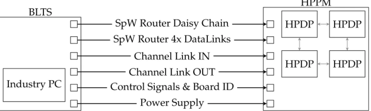
An HPDP chip must be placed on the main board, which provides ports and slots for in- terfaces and external memories. For test purposes, the board needs further connections to a master tester to send commands the HPDP then. Even though a real HPDP demonstra- tor chip is not supplied during the implementation, the commissioning tests must regard the provided test setup.
Figure 4.2 depicts the test setup including a test system, a board, and an HPDP chip. The test system runs on a Board Level Test System (BLTS) that is explained in the following subsection. The depicted board is a multi-chip board that has slots for up to four HPDP chips. Both, single-chip and multi-chip board are in development, and they are described afterwards.
4.2.1 Board Level Test System (BLTS)
An HPDP chip will be tested with the provided Board Level Test System (BLTS) that in- cludes an off-the-shelf industrial computer for manual testing and automated test execu- tion. The HPDP BLTS is designed for testing maximum data throughput of the HPDP module. Required software and hardware modules are installed. A front-end application manages the communication between the HPDP board and a UMDS Runtime System (Universal Data Management System). UDMS is a generic database driven tool and ap- proved in many space test system projects. The off-the-shelf industry PC has an Intel Core i5-4570 CPU with 16 GBytes RAM. [Bro15]
Industry PC BLTS
HPDP HPDP
HPDP HPDP
HPPM SpW Router Daisy Chain
SpW Router 4x DataLinks Channel Link IN Channel Link OUT Control Signals & Board ID
Power Supply
Figure 4.2: A simplified representation of the HPDP-BLTS (Board Level Test System) envi- ronment including the High Performance Processing Modul (HPPM) with four HPDP chips. [Bro15]
With such a test system, a manual command or even an automated test script can read or write, if possible, every accessible register of the HPDP via the Daisy Chain and the HPDP SpaceWire module. Thus, the system can configure the HPDP chip, copy a program into
4 Test concept
code memory, test specific functions by static access, start the boot process, or monitor a whole program execution only via the SpaceWire connection.
Further, high-speed SpaceWire DataLinks and Channel Links are available to simulate the data transfer of on-board instruments. Each of the Channel Link IN and OUT utilises one Stream-IO port. Also, a board has an ID that is readable from GPIO pins by the HPDP chip. The BLTS environment can assign every board a unique ID as board chaining is planned in future.
4.2.2 Single-chip Board
The single-chip board is the preferred one for commissioning of the first delivered HPDP chip. It offers all necessary ports for the HPDP interfaces and contains two fixed board memories. At port 0 is an 1 Mbyte EEPROM interconnected and should mainly be used as code memory since the write speed is slower than SRAM or SDRAM. The latter memory type is linked to memory port 1 and provides 512 Mbyte storage capacity for the HPDP chip.
Besides the SpaceWire Daisy Chain, data can also be transferred from and to the board by a SpaceWire DataLink, or by a ChannelLink IN and ChannelLink OUT. Thereby, only the Stream-IO ports 0 and 2 are used. The other two ports are interconnected to a loop back.
That means that data send to Stream-IO port 1 is transmitted to port 3 or vice versa.
Moreover, the single-chip board utilises six GPIO (General Purpose Input/Output) pins of the HPDP chip. The first two pins are used to activate the ChannelLink or SpaceWire DataLink connections, and the next three pins can steer three LED lights. All of them are used as output by the HPDP. The last pin is an input pin for reading the board ID bitwise.
Appendix A.1 contains a tabulated overview of the technical data of the HPDP chip.
4.2.3 Multi-chip Board (HPPM)
Up to four HPDP chips can be placed on a multi-chip board called High Performance Processing Module (HPPM). All four chips are connected to a ring structure using two Stream-IO ports. Another Stream-IO port of each chip can be linked to another HPPM, and the fourth port is connected to a Channel Link. Further, the GPIO assignment and both board memories are equal to the single-chip board.
This work comprises a commissioning test software for the first demonstrator chip, and the single-chip board is firstly delivered and sufficient. Multi-chip programs are out of scope, and the tests shall primary be designed for one processor chip. Nevertheless, the operational capability for multi-chip testing is shortly discussed in section 5.4.
28
4.3 Test strategy
Figure 4.3: Events per second in a target system for different abstraction layers [ESL01]
4.3 Test strategy
The beginning of this chapter introduced different approaches in processor testing. The conclusion is that one essential characteristic of a test program is running at operational speed since sensitive timing affects only arise when the chip runs under that condition.
SBST is a proper approach to reach that goal.
Another advantage of system-level testing, like SBST does, illustrates the figure 3. Due to the high abstraction level, fewer visible events occurs in a second what motivates a top- down testing strategy. Testing at the register-transfer level, or even harder on gate level increases the number of events to handle and also the number of checks if an error has occurred. This section describes the test approach in detail.
4.3.1 Source and sink pattern
Wrapper Embedded
core Sink
Source test access mechanism
test access mechanism
Figure 4.4: Source and sink pattern for testing an embedded core; a test sequence (or pro- gram) is transferred via a test access mechanism from a source to a wrapper that includes the core-under-test; the respond is forwarded to a sink [ZMD98]
The procedure of the SBST methodology can be nearer described by the source and sink pattern introduces in [ZMD98]. Figure 4.4 shows an architecture composed of three struc- tural elements. The first component contains the source that generates the test patterns, and the sink, that compares the response to the expected result. The second element, the test access mechanism, transports the patterns from the source to the core-under-test
4 Test concept
and the produced responds back to the sink. The central feature is a wrapper forming an interface between the embedded core and the test environment.
This pattern can directly be mapped to the given test setup where the source and sink rep- resent the external tester (BLTS). The SpaceWire and Channel Links are equal to the test access mechanism, and the wrapper stands for the single-chip board (or multi-chip board).
The tester loads an FNC-program into the code memory through the serial SpaceWire in- terface and waits for the response of the HPDP chip, sent via SpaceWire likewise. Hence, the illustrated pattern is a black box testing technique.
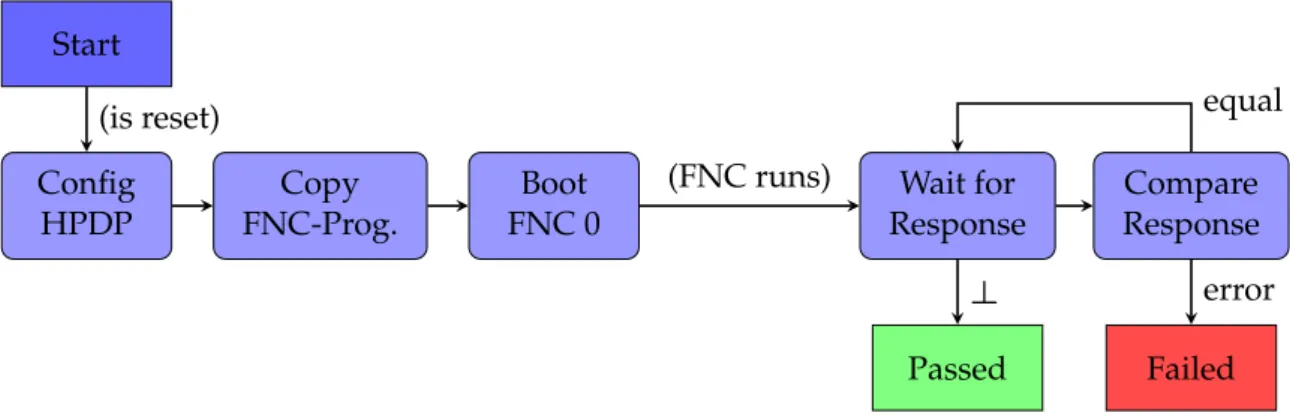
4.3.2 Procedure of a single test program
Start
Config HPDP
Copy FNC-Prog.
Boot FNC 0
Wait for Response
Compare Response
Failed Passed
(is reset)
(FNC runs)
equal
error
⊥
Figure 4.5: Test program flow of the script file. Each test program should start after a reset, and initialize the HPDP as required. The wait sequence for the HPDP responses follows after the boot. Finally, the results are evaluated.
The control flow of the source and sink pattern can be either executed manually by a test user or represented in a script that includes all instructions for the BLTS from the begin- ning until the end of a single test program. A script has several advantages compared to manual work. Repetitive and redundant work can be combined in a file to provide a com- mon basis for simple maintainability and reusability. A typical test sequence of a script is illustrated in figure 4.5.
Every test program shall start after a reset of the HPDP chip to avoid side-effects between consecutive programs. A reset can be accomplished by disconnecting the power supply which sets all registers back to their default values. The configuration of the processor is the first step and takes a few milliseconds so that a reset should not be an obstacle. When the HPDP is in the intended state, the tester can start copying the FNC-program into the code memory and initiate the boot process. While the FNC runs, the tester (sink) waits for the responses and compares them with the expected result. A test case fails if at least
30
4.3 Test strategy
one result does not match the one expected. Otherwise, it has passed.
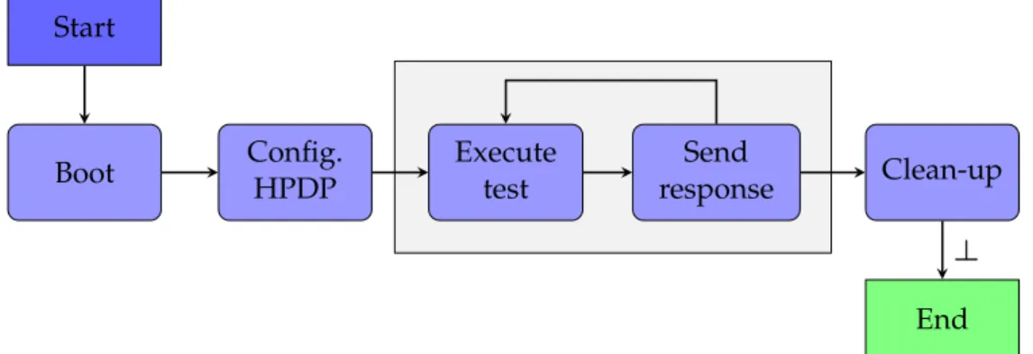
Figure 4.6 depicts a typical test sequence for the embedded chip. After the boot instruc- tion reaches to the HPDP, it starts with fetching the first instructions from code memory and executing them. Those instructions usually include the default configuration actions, contained in the boot code library. Also, each FNC program includes specific configu- ration instructions which are required by the test case. Next, the program executes the programmed test sequence, which includes sending back one or multiple responses via SpaceWire to the tester. Finally, the system is cleaned up. That last step could be omitted since the next test starts after a reset.
Start
Boot Config.
HPDP
Execute test
Send
response Clean-up
End
⊥
Figure 4.6: Each FNC-program starts with a configuration of the HPDP, continues with the intrinsic test sequence and clean up the system at the end. A test sequence may send messages to the external tester.
4.3.3 Sequence of several programs
A couple of test programs are required to cover all analysed, possible problem. Of course, one huge test might treat everything, but this is not beneficial for the test user regarding maintainability and reusability. In particular, some tests need to run several times with different parameters to cover everything. That concerns memory tests as test user may diverge from what is important and what is not. Besides, it does not make much sense to run two or more different tests on the same chip in parallel since side-effects or limited resources would affect the test results.
Incremental integration testing
The commissioning has to deal with a couple of problems. On the one hand, there could be HPDP specific internal issues, and on the other, an interface connection with the board
4 Test concept
and the external tester could not work properly. Since a verification of an HPDP feature requires working interfaces, the order of tests should be planned carefully. That could simplify the classification of errors as previous tests have indicated that individual com- ponents work presumably. Big-bang testing does not make much sense here and therefore the chosen approach is inspired by incremental integration testing. In this method, every following test extends the number of tested modules with the least components as possi- ble.
Advanced strategies
Researchers have introduced some advanced strategies like a tree structure for extracting a distinct fault from overlapping tests [BHF96]. There, each test is related to a couple of sub- tests which are executed if the test fails. Further, a smart tree structure with the knowledge about possible errors of each test could then be used to spot the defect accurately. As the analysis section already discussed, an advanced strategy is out of scope for commissioning and a simple sequential order is sufficient. Additional detailed tests can be performed by the JTAG interface to investigate the origin of an arisen fault.
4.3.4 Memory testing
The HPDP architecture includes several internal and external memories, supporting al- gorithms with different storage strategies for big data sets. Each memory contains a BIST structure for comprehensive memory tests during manufacture or running in debug mode.
Usually, a RAM module comprises a memory cell array, an address decoder circuit, and a read-write circuit. A wide-spread memory test technique finding all known faults in SRAMs is the algorithm "length 9N" (included faults are: memory cell stuck-at-1/0 faults, stuck-open faults, state transition 1-to-0 and 0-to-1 faults, state coupling faults to another cell, multiple access and wrong addressing faults, and data retention faults). [TNF01]
Even though the internal functionality of each memory seems to be sufficiently tested, the functional integration into the HPDP environment and the functional connectivity have to be verified. For instance, the interaction between the SYSMEM arbiter and a board mem- ory address decoder is not tested by BIST and both components are separated while man- ufacturing. However, the SYSMEM arbiter is tested using boundary-scan-chains before commissioning. A simple test strategy looking for multiple accesses and wrong address- ing faults should be sufficient. Section 5.3.1 discusses an adequate implementation.
32
![Figure 2.4: A FNC-PAE includes eight ALUs arranged in two colums, a Special Functional Unit (SFU), 16 bit registers, 32-bit address generator (AG) and a L1 Instruction cache and data cache [PAC09g]](https://thumb-eu.123doks.com/thumbv2/1library_info/4355434.1575408/21.892.251.605.166.338/figure-includes-arranged-special-functional-registers-generator-instruction.webp)
![Figure 4.1: Possible crosstalk faults in integrated circuits which must be tackeled at oper- oper-ational speed of the processor [BCD03]](https://thumb-eu.123doks.com/thumbv2/1library_info/4355434.1575408/38.892.179.745.210.477/figure-possible-crosstalk-integrated-circuits-tackeled-ational-processor.webp)
![Figure 4.3: Events per second in a target system for different abstraction layers [ESL01]](https://thumb-eu.123doks.com/thumbv2/1library_info/4355434.1575408/41.892.241.614.168.340/figure-events-second-target-different-abstraction-layers-esl.webp)