Electrochemical processes for design and modification of interfaces and
surfaces of electronic devices
A Dissertation Presented for the Degree of Doctor of Natural Sciences
(Dr. rer. nat.)
At the Natural Sciences Faculty IV Chemistry and Pharmacy University of Regensburg
Edmund Riedl Regensburg 2014
Official Registration: 18.06.2014
Defence: 22.07.2014
Supervisor: Prof. Dr. H. J. Gores
Adjudicators: Prof. Dr.R. M. Gschwind; chair Prof. Dr. H. J. Gores
Prof. Dr. W. Kunz Prof. Dr. J. Daub
For Martina, Johanna and Theresa
Schreite beschwingt voran und akzeptiere kein „Geht nicht“.
Rechne mit wunderbaren Lösungen.
Mystique
Acknowledgements
This work was only possible with the continuous help and support of many people.
First I want to thank Prof. Dr. Heiner-Jacob Gores for his never ending encouragement on the structuring of this work and document. He basically was the bridge between academic approach and industrialization of the described technologies and the heart of this dissertation within the workgroup “Electrochemistry and Electrolytes” at the University of Regensburg.
Prof. Dr. Werner Kunz, chair of the Institute of Physical and Theoretical Chemistry, offered me a place to work in his laboratories and enabled a lot of results from University of Regensburg in addition to the vast amount of data gained within Infineon AG in nearly one dozen of successful cooperation projects with his organisation.
As the father of the industrialization of this works and the soul of the technology I want to thank Dr. Helmut Strack from Infineon AG with his never ending hunger for discussions and the continuous believe in my success.
Finally I want to thank all the colleagues at University of Regensburg and at Infineon worldwide for their support and cooperation, my colleagues! Steve T., Tobias S., Franz W., Franz K., Steffen J., Johannes L., Arno Z., Robert B., Loo EH, Wong FH, Badrol H., Mohtar, Jagen, Lit HK, Rudolf S., Karl M., Andreas R, Josef M. and all the others.
Thank you for guiding me through the ups and downs of this work.
And finally the most thanks I have to give to my ever supporting family Martina, Johanna and Theresa always putting a smile on my face at each time of the work. I love you.
Abstract
This work describes several approaches and two major advances obtained by numerous studies on the areas of semiconductor packaging technologies including adhesion promotion technology and copper surface design for interconnect techologies. This work was partially performed during the last decade in collaboration with the workgroup “Electrochemistry and Electrolytes” at the University of Regensburg, Institute of Physical and Theoretical Chemistry, chair Prof. Dr. W. Kunz. All analytical work and investigations on processes and manufacturing technologies was done at Infineon AG at different locations worldwide.
In the first main part both the design and development of adhesionpromoter technologies for semiconductor devices is reviewed. The focus is put on electrochemical deposition of nanostructured adhesion promoters.
The results of this work were the industrialization of the deposition of a Zn-Cr alloy as a nanoporous adhesion promoter after assembly of the semiconductor device right before encapsulation. As an important innovation, the deposition of the adhesion promoter was successfully performed on all metallic surfaces of the chip and the package including aluminium chip metallisation, leadframe, solder and interconnect wires. Particularly activation of aluminum for the subsequent electrochemical deposition of Zn-Cr alloy was a major resolved challenge besides various aspects of the deposition process itself.
Results are reported on deposition mechanisms for obtaining a nanoporous layer by electrochemical deposition.
In addition, respective process investigations are described to gain a best-in-class adhesion promoter technology for highly reliable power semiconductor devices including finally the integration of this technology into the manufacturing process flow.
As further major developments new electrolytes were obtained by these works enabling the withdrawal of unwanted and environmentally detrimental chromium-VI species in the process and improving plating homogeneity as well. These novel examples include electrolytes for Zn-Mo and Zn-V alloys.
In the second part presented as an addendum, the surface design of copper with organic molecules is reported. These organic coatings are preventing uncontrolled oxidation of copper and are therefore prerequisites for processing copper surfaces during soldering or during copper wirebonding. A short review of the copper oxidation kinetics is given as well. The efficiency of oxidation protection of copper coated with 1H-benzotrialzole, mercaptobenzimidazole, decanethiole, poly(1-vinylimidazole), poly(4-vinylimidazole) and poly(benzimidazole) is discussed. The application to either soldering processes or copper wirebonding was shown and an outlook is given for the usage of organic molecules as Cu passivations in these applications.
To sum up, various advances have been reached some have already been included in current production processes. Suffice it to mention that also several novel aspects were studied that may be usefull for future progress.
Table of content:
1 Motivation for interface and surface design for electronic devices ... 17
1.1 Introduction ... 17
1.2 Basic fatigue mechanisms within a power semiconductor device ... 19
1.3 Fatigue of the chip ... 21
1.4 Fatigue of the package ... 23
1.5 Measures to prevent fatigue in a power semiconductor device ... 30
1.5.1 Chip related measures ... 31
1.5.2 Package related measures ... 33
1.6 Focus of this work ... 41
2 Analytical and experimental methods ... 42
2.1 Field emission scanning electron microscope (FESEM): Surface morphology ... 42
2.2 Energy dispersive x-ray spectroscopy (EDX) ... 47
2.3 Transmission electron microscopy (TEM) ... 48
2.4 Button shear test ... 49
2.5 Tape adhesion test ... 50
2.6 A2 dip test ... 53
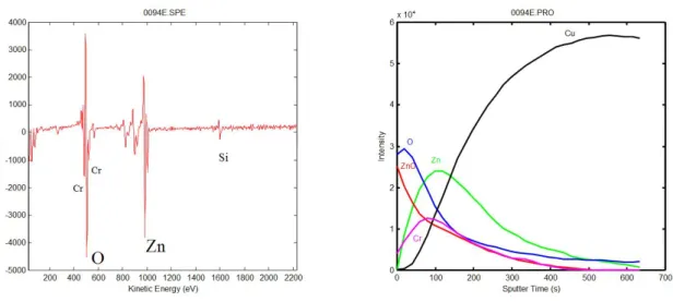
2.7 Auger electron spectroscopy (AES) ... 54
2.8 X-ray photoelectron spectroscopy (XPS) ... 58
2.9 Time of flight secondary ion mass spectroscopy (TOF-SIMS) ... 61
2.10 Scanning acoustic microscopy ... 64
2.11 Solder wetting balance for measuring wetting force-time-graphs ... 66
3 Adhesion promoter: Identification of A2 process as the target technology for adhesion in a MOSFET package. ... 68
4 Theoretical background and models for the understanding of dendritic depositions ... 76
4.1 Activation of metal surfaces ... 76
4.1.1 Properties and states of the different surfaces prior to activation ... 76
4.1.2 Activation of Cu surfaces ... 83
4.1.3 Activation of Ni and NiP surfaces ... 87
4.1.4 Activation of Pb-2Sn-2.5Ag solder surfaces ... 95
4.1.5 Activation of aluminium chip surfaces ...101
4.1.5.1Reactions of the aluminium metallisation: Oxidation and corrosion ...101
4.1.5.2Activation of Al2O3 with an Ar/CF4 plasma process ...108
4.1.5.3Activation of Al2O3 with aqueous HF / MSA chemistry ...109
4.2 Theory of the electrochemical deposition of a porous layer ...115
4.2.1 Basics for electrochemical deposition ...115
4.2.1.1Electrode potential and overpotential ...115
4.2.1.2Kinetic mechanism of deposition with reaction control ...122
4.2.1.3Kinetic mechanism with mass transport control ...126
4.2.1.4Deposition of alloys ...130
4.2.1.5Current efficiency and concurring reactions ...134
4.2.2 Electrolyte chemistry for A2 deposition and comparison to other electrolytes ....135
4.2.3 The deposition of zinc ...136
4.2.4 The chemistry of chromates and the deposition of chromium ...141
4.2.5 Chromate conversion coatings (CCCs) on zinc ...143
4.2.6 The deposition of Zinc - chromium alloy ...144
4.2.7 Chemistry and function of silicate: Co-deposition of SiO2 ...148
4.2.8 Mechanisms of deposition kinetics for porous and dendritic electrodeposits ...149
4.2.8.1Dendritic growth via mass transport controlled deposition ...150
4.2.8.2Dendritic growth via surface inhibition followed by mass transport controlled deposition ...156
4.2.8.3Dendritic growth via surface topology and mass transport controlled deposition ...156
4.2.8.4Dendritic growth by electrophoretic deposition with silicate carrier. ...157
5 Deposition of A2 layer: Experimental results of the development of an industrial process ...160
5.1 Overview on the A2 process and technology ...160
5.2.1 Investigation of activation with H2SO4 and MSA (er81 and er98) ... 163
5.2.2 Investigation of the influence of oxidation during chip soldering on deposition of A2 (er175) ... 166
5.2.3 Argon / CF4 plasma process for activation of the Al chip metallization (er265) .. 169
5.2.4 Integration of Ar / CF4 plasma process for activation of the Al chip metallization in the process flow (er269, er270) ... 186
5.2.5 Aluminium activation in A2 process with HF chemistry and Ar / O2 plasma conditioning of wafer ... 195
5.2.6 Further work and development of fluorine free alternative conditioning of Al-1Si- 0.5Cu ... 199
5.2.7 Summary of activation procedures ... 201
5.3 Deposition of A2 with constant current ... 203
5.3.1 Overview on deposition parameters ... 203
5.3.2 A2 layer characterization and properties ... 204
5.3.3 Electrolyte for A2 process and chemical interactions ... 207
5.3.3.1Preparation of the electrolyte for A2 deposition ... 207
5.3.3.2Characterization of the electrolyte ... 209
5.3.4 Influence of the concentration of the various electrolyte species on the morphology of A2 deposit. ... 210
5.3.5 Influence of deposition current density ... 217
5.3.6 Hydrodynamic influence: Electrolyte flow and transport belt speed ... 224
5.3.7 Cell design for A2 deposition ... 230
5.3.7.1Cathode shield tube: Design of geometry and flow of electrolyte for TO220 leadframe (er228)... 230
5.3.7.2A2-Cell: Design of geometry of plating cell for TO263 leadframe (er309). .. 232
5.3.8 Summary on A2 deposition ... 239
5.4 Environmental measures for A2 technology... 241
5.4.1 Wastewater treatment to prevent chromium-VI emission ... 241
5.4.2 New chromium-VI free electrolytes for A2 process in the future ... 243
5.4.2.1Chromium-VI free alkaline zincate electrolytes for A2 deposition ... 244
5.4.2.2Chromium-VI free acidic zinc electrolytes for A2 deposition ... 265
5.4.3 Summary and and outlook on Cr-VI free electrolytes for A2 deposition ...270
6 Addendum - Organic coatings of surfaces for prevention of copper oxidation ...272
6.1 Applications of copper and its limitations due to oxidation ...272
6.2 The Oxidation of copper ...274
6.3 Organic materials for copper passivation ...277
6.3.1 Application of benzotriazole for copper passivation of semiconductor device terminals for PCB soldering ...277
6.3.2 Application of poly(vinylimidazole) for copper passivation for copper wirebonding on copper metallisation ...285
7 Summary, publications and outlook ...295
7.1 Main part: Nanoporous adhesion promoter in semiconductor packages - A2 technology ...295
7.2 Addendum: Organic coatings of surfaces for prevention of copper oxidation ...300
8 Abbreviations and acronyms ...303
9 Curriculum Vitae ...305
10 Literature ...307
1 Motivation for interface and surface design for electronic devices
1.1 Introduction
Looking at the past decade it can be seen that the effort in semiconductor industry is undergoing a shift towards systems with high energy efficiency driven by miniaturization of products. Miniaturization of power semiconductor devices means for example shrinking energy stores for the individual device that reduces switching losses.
Besides energy efficiency there is an increasing demand for electric power management of electronic for automotive, industrial and commodity products. A booming area in this field is the renewable energy technology including wind-powered generators, photovoltaic devices (solar cells), and see water-powered generators; all are demanding of highly reliable and efficient power semiconductor products. These requests speed up the trend to miniaturization and reliability as key drivers for power semiconductor devices. Example given, Figure 1 shows the dramatic advances of technology of MOSFET (metal oxide semiconductor field effect transistor) devices in the first half of the past decade taking one technology step every two years and a chip size approximately halved each step. In addition production volume of power semiconductor devices has increased, too.
Figure 1 : Shrink path for power semiconductor technology: From year 2000 until 2005 three technology steps have been accomplished in contrast to the time before 2000 (source: Infineon MOSFET roadmap).
Also the realization of environmental directives like the RoHS (Restriction of hazardous substances) and WEEE (Waste of electrical and electronic equipment) directives by mainly the switch from Pb-Sn PCB (printed circuit board) solder with melting temperatures of Tm=179°C to Sn-Ag or Sn-Ag-Cu alloys with melting temperatures of Tm=221°C is addressing higher reliability to devices. It brings up much higher PCB soldering temperatures of up to 260°C peak temperatures of course with some consequences to semiconductor device stressing during manufacturing of the application on PCB. The increased thermal stress at PCB soldering is leading to a much higher pre-damage to power devices and bringing the risk of lower lifetime reliability.
From this point of view the environmental laws such as the WEEE- and RoHS- directives and product requirements have enforced innovations and brought out next generation product reliability for power semiconductor devices needed for further high temperature applications for future applications. In figure 2 the benefit of electronic devices within cars can be seen. Shown are safety improvements in comparison to the increasing number of cars within the last decades. The increasing complexity of electronic components is increasing efforts for reliability of the individual device in order to make the complete system more reliable. If the complete system in the car has to be highly reliable the individual devices for building the system require zero defect density to minimize multiplication of defects. In order to develop and to manufacture a highly reliable device a couple of failure mechanisms need to be understood first to identify the major fatigue chain in a power semiconductor device. This chain will show that there are major approaches possible to design interfaces and surfaces via electrochemical processes to help to design reliable electronic devices.
Figure 2: Overview of development of deathly casualties from 1950 until 2005[1].
1.2 Basic fatigue mechanisms within a power semiconductor device
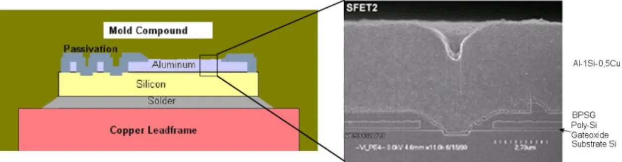
To understand the basic failure mechanisms within a power semiconductor device first the simplified structure of a device is explained. The package of a power semiconductor device consists of many different materials and interfaces as shown in figure 3 . Almost every device uses polymer based mold compounds and metal based leadframes, common is the use of Cu with different plating such as Ag, Ni or NiP alloys (nickel/phosphorus). The top of the semiconductor chip is coated with an Al based metallization and by the isolating passivation, mostly SiN (silicon nitride), opened at the bond windows to get an Al surface towards the package. Underneath the Al layer there are other layers depending on the semiconductor device. For a MOSFET device BPSG (boron-phosphorus-silicon-glass), polycrystalline silicon and finally the gate oxide (SiO2) is located there on top of the silicon substrate of the chip.
Figure 3: Structure of a powersemiconductor device which shows the geometry and the different interfaces.
The device is undergoing various process temperatures during specific manufacturing processes. For example two major thermal budgets are applied during chip soldering at θ=400°C and during the molding of the device with mold compound at 180-200°C.
Cooling down the device to room temperature after the individual process already implies stress due to CTE (Coefficients of linear thermal expansion) mismatch of the different materials within the device. Table 1 shows the differences of the CTE and elastic modules (E) of the used materials.
Material α [10-6 K-1] E [109 N*m-2] = [GPa] Note
Silicon Si, [2] 2.9 (273-1673K), 112 298.15 K
Copper Cu, [2] 16.5 128 298.15 K
Aluminium Al, [2] 23.0 70.3 298.15 K
Mold compound KMC 2110G-7, [3]
α1=13 E1=18.5 α1 at θ<θG=133°C
E1 at θ=25°C Mold compound
KMC 2110G-7, [3]
α2=51 E2=1.5 α2 at θ>θG=133°C
E2 at T=150°C
Table 1: CTE (Coefficients of linear thermal expansion) and elastic modulus (E) of different materials used within a semiconductor device, mold compound data also in [4].
The different CTE cause a lateral stress at various interfaces. For example during cooling down a device from a molding process temperature of 180°C to -55 °C during cold testing of the device in the production line the geometrical mismatch between mold compound and silicon is already 4 µm per 1 mm length of interface (0.4%). The residual stress is concentrated at the interfaces between the specific materials, hence interface damage due to CTE mismatch during temperature cycling is one very common fatigue mechanism in a semiconductor device. This interface fatigue is generating secondary fatigue mechanisms. Primarily the interface fatigue can be detected as a delamination
between two subsequent materials which is analysed by SAM (scanning acoustic microscopy).
1.3 Fatigue of the chip
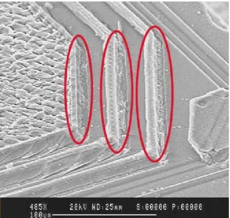
As the molding compound has more than 5 times the CTE of Si below the glass transition temperature (Tg) the polymer brings a high stress on the chip top during heating and cooling. Additionally the mechanical properties of the molding compound are changing dramatically below Tg and at lower temperatures which can be seen in table 1. The elastic modulus increases by more than factor 10 comparing E1, 25°C = 18,5 GPa and E2, 150°C = 1,5 GPa. Hence the stiffness of the molding compound is increasing strongly during cooling. Together with the high CTE this leads to deformation of metal lines and to a even complete removing of metal lines after several temperature cycles, finally to electrical fail through shortages or cracks. Figure 4 shows a FESEM (field effect scanning electron microscopy) picture of this fatigue on a device which is having an aluminium metallisation without passivation. Results will be shown later how this fatigue can be prevented.
For the passivation of the frontside metallisation of the chip and structures usually a silicon nitride layer (SiN) is used. The above mentioned shift of aluminium metal layers below the SiN happens with a high plastic deformation rate during applying temperature cycles. This can lead to SiN passivation cracks which then are starting points for corrosion giving a path for humidity to diffuse down to the aluminum layer [5]. In figure 5 an example is given, a FESEM picture is shown with a 800nm SiN layer on aluminium lines showing cracks which can go deeper into layers underneath the metal layers leading to immediate electrical fails.
Figure 4: Shifted aluminium metal lines after 1000 TC (temperature cycles) from -55 °C to 150 °C on a MOSFET power device in a TO263-3 package.
Figure 5: Passivation cracks over metal areas after 1000 temperature cycles (-55°C to 150 °C)
1.4 Fatigue of the package
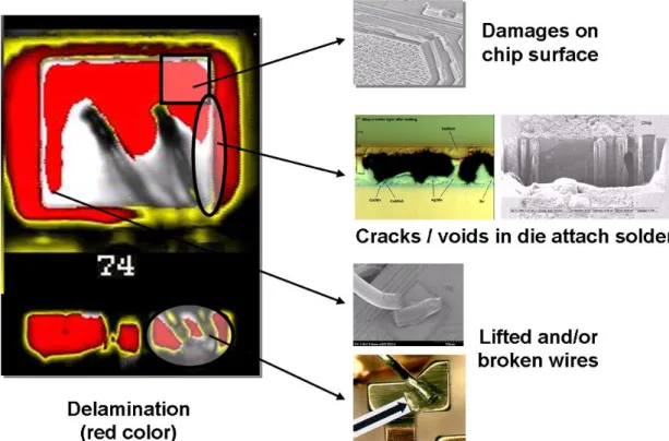
Not only the chip but also the package of a device has several interfaces, especially critical interfaces are those between polymers and metals. This interfaces are so critical as polymers are not chemical bonded strongly to metals as compared to a crystalline interface between two metals forming for example intermetallic phases. Therefore, those polymer to metal interfaces are the weak link in the system. Damage of this interfaces, which is basically called delamination and popcorn cracking in the package leads to several secondary fatigue mechanisms, some of them are shown in figure 6.
This delamination occurs already during the hot PCB soldering process which is done for example at temperatures of 245°C up to 260°C.
In addition to major fatigue of the chip front side the chip backside interconnect fails through solder- or glue cracking. Cracking of the wire interconnects happens toward the chip frontside as well as toward the package on the leads. Finally all these effects lead to drift or fail of electrical parameters and therefore entail an instable or failed device.
In the following section some examples will be given showing that the major problem in plastic packages is the adhesion of the molding compound to the rest of the device. In figure 6 some examples of fatigues can be seen which all are primarily generated by a delamination of the molding compound.
Chip backside interconnect fatigue (e.g. solder)
Solder fatigue can be differentiated into two modes:
a. Melting of the solder alloy due to temperature overstress.
b. Cracking of the solder due to thermo-mechanical stress.
The mechanism of melting can easily be explained for alloys which are unsuitable for high PCB soldering temperatures. An example is shown in figure 7, Sn-25Ag-10Sb (alloy-J) is melting during 260°C board soldering resulting in big voids in the solder layer. These voids reduce the thermal coupling of the chip to the package heatsink and lead to overheating of the device during operation.
Figure 6: Failure mechanisms in a strongly delaminated package leading to electrical failues during livetime of a product.
Figure 7: The solder alloy Sn-25Sn-10Sb (“alloy-j”) melts at a temperature of Θm=228°C leading to voids. This is a consequence of the high PCB soldering temperature of 260°C.
The mechanism of solder cracking is explained first by thermomechanical stress during
creeping in the softer solder alloy. This creeping is additionally enforced by the molding compound especially in asymmetric packages with strong delamination. There the molding compound can apply forces to the chip leading to creep in the solder.
Looking at the available solder materials and the prerequisite from metallurgy for the requirement of 260°C PCB soldering from industry Pb-Sn-Ag (Pb content >90 weight
%) alloys are offering a high melting temperature with the disadvantage of a lower creep resistance especially at higher temperature. During temperature cycle stress the creeping of the alloy leads to formation of voids at the grain boundaries which finally leads to crack propagation from void to void along the grain boundaries. For those soft solder alloys this weakness is a technological limitation which can be compensated in the package only by supporting the chip with a high adhesion of the molding compound so that plastic deformation of the solder is minimized during lifetime of the device.
Void formation during thermomechanical stress is already degrading the thermal connection of the chip backside to the package heatsink leading to drift of parameters.
Figure 8 shows a FIB (focused ion beam) cut through a solder layer after a thermomechanical stress of 1000 temperature cycles from -55°C to 150°C. Voids between the grains of the solder are located especially besides the chip and its backside metallisation.
Figure 8: FIB (focused ion beam) cut on a cross section of a solder layer which shows solder crack after TC500 (-55 to 150°C) already. The analysis shows voids between the different crystallites of the solder. The x-section was done along the red line in the SAM picture below, the FIB cut was done on position 1 in the SAM picture.
The behavior of such degrading devices is shown in figure 9. During several package evaluations stress tests were done on standard devices and on devices with an adhesion promoter technology. The groups with low adhesion along the stress tests shows strong delamination of the molding compound and huge void formation within the solder layer in the SAM. Related to the voids also the electrical parameter measured in this experiments show strong drift after the respective stress tests proving the degradation of the thermal connection between chip backside and package heatsink.
Stability of electrical parameter: DVSD in Robust Package
DVds: ER93-C_Ref; Pb-2Sn-2,5Ag-0,02P, 30mm², no A2;
0 20 40 60 80 100 120 140
initial precon 500c 1000c 2000c
h ours mV
Pb-2Sn-2,5Ag; DVSD; 30m m² on NiP with A2
0 20 40 60 80 100 120 140
initial precon 600c 1100c 2100c
h ours mV
Strong adhesion at all interfaces prevents solder delamination
during 2100 temperature cycles:
No DVSD-drift TO263-3 with strong
delamination of moldcompound
TO263-3 with full adhesion after A2-treatment Low adhesion leads to
solderfatigue already after 500 temperature
cycles:
strong DVSD-drift
Figure 9: Top: Interface degradation leads to fatigue of the solder and therefore to a fail of the thermal contact between chip and package. This leads to a electrical drift of the DVSD parameter. Bottom: No solder degradation, no drift of the electrical DVSD parameter.
Wire-Interconnect fatigue
Besides the chip solder the delamination of molding compound also affects the wire interconnects at the frontside of the chip. There are basically two categories of wire interconnects in power semiconductor packages:
a. Homogenous systems such as Al/Al, Au/Au or Cu/Cu.
b. Heterogeneous systems such as Al/NiP; Au/Al; Cu/Al.
Within the homogenous systems the metal-to-metal adhesion is only driven by interdiffusion, there are no metallurgical reactions running as both partners consist of identical metals even if there are slight differences in doping. Therefore interconnects with homogenous systems do not show metallurgical degradation mechanisms.
In contrast, heterogeneous systems can form several intermetallic phases which in some cases are not favored due to degradation, in some cases are favored as they offer a very
strong crystalline interconnect. Contacts of Au wires on Al metallisation for example show a decrease of the mechanical strength of the interconnect during formation of several intermetallic phases such as Au4Al, Au5Al2, Au2Al, AuAl and AuAl2 especially at a temperature above 150°C [6].
In addition to metallurgical degradation mechanisms of wire interconnects, a additional failure mode specifically for heterogeneous systems is corrosion. As different metals are in contact to each other contact corrosion together with humidity leads to ion movement and fast oxidation of the less noble partner (e.g. Al dissolution in the system Al/NiP).
This can happen during the manufacturing of the device in wet chemical processes and also during the lifetime of the device. Delamination of molding compound is the starting point which leads to open paths between ambient humidity and the interconnect.
Finally, in addition to metallurgical and electrochemical degradation mechanisms which mainly lead to a decrease of the mechanical strength of the interconnect one of the major fatigue risks for all bond interconnects is mechanical stress due to delamination of the molding compound to the device. This leads to shear and pull stresses on wires and finally to breaking of the already weakened bond contact. Figure 6 shows two example pictures.
Also for the interconnects on the chip frontside adhesion of the molding compound is an important factor to maintain stable wire bond contacts.
Degradation of package interfaces
A pure polymer (either duromer or thermoplast) has only a weak interaction to inorganic surfaces (e.g. metals, oxides, nitrides) by Van-der-Waals forces or via hydrogen bridges. Therefore most molding compounds are coming with bifunctional additives engaging a stronger bonding towards inorganic surfaces (e.g. tri-ethoxysilyl functions). There is a high number of adhesion enhancing technologies either intrinsically inside the molding compound with bifunctional molecules as well as dedicated adhesion promoters or primers which are applied to the surfaces of the chip and the leadframe prior to molding.
Fatigue at the interface can happen at the leadframe, for example through cracking
molding compound along the interface. Finally also the chemical bonds at the interface can disintegrate. The latter happens especially together with water. Water at high temperature is acting as a nucleophilic agent reacting with carbonyls and other electrophilic groups which are responsible for the interconnect. Water from ambient humidity diffuses into the molding compound towards the interface. Applying PCB solder heat is increasing the reactivity of water, its vapor pressure increases and that can lead to a sudden cracking of the interfaces which is known as popcorn cracking [7]
within a semiconductor device.
Degradation of molding compounds
The major parts of a molding compound are the resin and the fillers. Typically epoxy resins with SiO2 filler are used. The most frequent is an orthocresolnovolac resin (OCN). Catalysts accelerate the polyaddition of the oligomers during molding at temperatures of 170°C - 180°C. Elastifiers maintain elasticity in order to keep thermo mechanical tensions in the package low. Adhesion promoter molecules improve the adhesion of the molding compound.
Waxes are used to enable the release of the molded units from the mold tool. Carbon black lowers the resistivity of the molding compound which works against electrostatic loading and gives it its black color. Flame retardants like metal hydroxides, phophonates or red phosphorous lower the flammability. The tuning of all these components for processability and reliability of the molding compound is the challenge for compound and semiconductor manufacturers.
Increasing temperature on the molding compound is leading to several reactions. For instance 175°C with conventional molding compounds leads to accelerated decomposition of the flame retarding components, for example brominated aromatic substances. They form decomposition products which by themselves can act as nucleophilic and electrophilic reagents (Br+, Br radicals and Br-) for further decomposition. Corrosive products, e.g. bromine ions, can develop which lead to corrosion on bonds and chip metallizations [8]. Due to health restrictions such brominated aromatics are not used anymore since the semiconductor world has converted electronic devices to "green" products in 2006.
An important property is the glass transition temperature, which for most molding compounds lies within the range of 100°C to 200°C. The biphenyl systems are similar to the epoxy resin systems showing glass transition temperature within the range of 100°C to 130°C, the OCN (orthocresol novolac) molding compounds within the range of 130°C to 160°C, and multifunctional molding compounds such as naphthalene based resins in the range of 180°C to 200°C [4].
Also CTE rises once the temperature exceeds the glass transition temperature of a molding compound which leads to increase of the stress at the interfaces to the metals and ceramics of the device. Adhesion at the interfaces is weakened and molecular adhesion is thermally cracked.
1.5 Measures to prevent fatigue in a power semiconductor device
Current requirements on especially automotive semiconductor devices are high already and due to the increase of electric complexity in cars future requirements will be further increasing. Lead-free soldering application brought in higher PCB reflow soldering temperatures of 260°C at high humidity (260°C@MSL1/85/85%rel.hum.) already in 2006 which required the design of a robust product as described in this work. High temperature application will furthermore apply high thermal and thermomechanical stress to the package as well as to the chip.
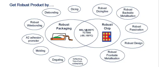
To overcome this challenge only a holistic strategy turned out to be successful in designing a robust product which is prepared to withstand also future stress. Figure 10 describes the elements within a semiconductor device and its manufacturing process which have to be addressed in order to make a product robust.
Figure 10: Robust Product - a holistic technical approach based on a new adhesionpromoter called A2.
1.5.1 Chip related measures
Chip related counter measures can be divided into three categories:
a. Material design of metallization b. Material design of passivation c. Geometrical layout of metallization
The interaction between metallization and passivation is mainly described by thermomechanical parameters like CTE and mechanical parameters mainly represented by yield strength. The yield strength indicates the change from the elastic mode to the plastic mode of the mechanical deformation. Increasing the yield strength of a metal line means to withstand higher stress without a plastic deformation, only elastic deformation happens which means that after the mechanical stress the metal line turns back to the initial shape.
As a metallization for aluminium technologies state of the art is to use Al-1Si-0,5Cu alloy. The requirements for this alloy are coming from the semiconductor itself and from manufacturing constrains as aluminium for frontside metallizations is mainly sputtered. For technologies with diffusion barriers also Al-0,5Cu is established as there is no requirement to add Si to the Al in order to prevent spiking between Si of the chip bulk material and the adjacent Al metallization. Therefore there are not very much possibilities to change the mechanical properties of the Al bulk material in the
metallization. Sputter parameters and annealing steps within the manufacturing process do have specific other constrains for other sections of the chip (cell geometry and edge coverage) so that a specific optimization of the Al bulk properties is very difficult.
Some semiconductor technologies are going the way towards sandwich structures sputtering several recurring Al and Ti layers in order to increase yield strength of the metallization. The more recent semiconductor technologies move completely away from Al and go for Cu based frontside metallizations. During development of the current robust product the alloy composition was not changed, but there were specific optimization regarding the sputtering of the Al metallization especially regarding minimization of Si precipitates in order to get a homogeneous distribution of Si grains within the metallization rather than a accumulation at any interface. This was basically reached by optimization of the sputter temperature profile during the whole process.
Major work has also been done on the design of the surface of the Al metallization, but the motivation here was not to increase the yield strength of the layer but to prepare the Al surface for the further adhesion promoter process which will be discussed in the individual section later.
For optimizing the material of the passivation there were two ways evaluated, the first way is to apply a silicon-oxy-nitride (SiON) instead of a SiN as SiON has a higher yield strength and therefore is not prone to cracking as what figure 11 shows. Increase of the yield strength by 50% showed no crack within this evaluation group.
Figure 11: Comparison of crack formation with passivation layers with a yield strength of 0,04 MPa*m2 (left side, SiN) and 0,06 MPa*m2 (right side, SiON).1
The second preferred option was to use a very thin SiN layer (40nm instead of 400nm) and cover this SiN with a 5µm polyimide layer. This system showed up the best reliability of the device and can be manufactured on standard equipment and processes.
Figure 12 shows the difference of the crack behavior of a standard 400nm SiN passivation with huge cracks and of a stack of 40nm SiN and 5µm Polyimide where there are only minor small cracks visible after a thermomechanical stress of 1000 temperature cycles (-55°C to 150°C).
Besides the change of the mechanical behavior of the different materials the geometrical layout of the layers also has a big influence on crack formation. It is well known that the stress on the chip surface is highest at the chip corners. New design rules were applied in order to avoid damage of chip surface also in chip edges and chip corners. Limits for maximum width and minimum distances of metal lines are one of the major rules. In case of multi layer metallization technologies the overlap of the different metal lines was fixed.
Figure 12: Comparison of crack formation between chips with 400 nm (left side) and 25 nm Silicon Nitride (right side). In order to investigate the SiN layer during opening and decapsulation of the device also the complete polyimide layer was removed.
FESEM pictures only show the surface of the SiN and the Al metallization.1
1.5.2 Package related measures
1 : Investigations done by Josef Maerz, Karl Mayer, Zechmann Arno, Kleinbichler Franz and the team.
Chip-backside interconnect
Besides the optimization of the backside metallisation, which was moved from a vapor deposition process to a sputter process in order to get a highly reproducible single wafer process, choosing of the correct solder alloy was one key factor.
One major criterion was the melting point which had to be above 260°C with a safety margin of at least 10°C. Technological standard today is to use high Pb containing Pb- Sn-Ag alloys with melting points between 280-310°C dependent on composition. The composition chosen was Pb-2Sn-2.5Ag as a compromise between wetting of the solder and reliability. Moving to higher Sn concentration is reducing reliability of the solder, voids are formed much earlier during thermomechanical stress. Reducing the Sn- concentration on the other hand side is decreasing the wetting of the solder as Sn is the reactive species on the used substrates like Cu or Ni. The chosen alloy offers a melting point of Tm=300°C, figure 13 shows a cross section of this solder in a device soldered on a Cu heatsink.
Figure 13: Ternary alloys are used for high temperature melting solders with
Tmelt=300°C. These alloys withstand a soldering temperature on PCB of up to 260°C.
Currently these high melting Pb-based alloys are the only solders worldwide which are suitable for being used for 260°C PCB soldering temperatures. All alloys with high Sn content which are used in PCB industry (e.g. Sn-3.5Ag; Tm=221°C) are melting below 260°C and therefore are unsuitable. There is still huge effort ongoing from the whole
The known weakness of these solders is due to their soft mechanical properties, they easily undergo creep fatigue especially during temperature cycling stress. This technological limitation of the used solder alloy can currently only be compensated by minimizing shear stress to the chip and finally to the solder and to minimize creepage.
In order to achieve this, the package has to have a hermetic encapsulation without any delamination of molding compound. This makes sure that the molding compound stiffness around the chip is also stiffening the solder layer. At this point it can be seen that an adhesion promoter is required on all surfaces interacting with the molding compound to achieve this stiffness.
Wire-interconnect
Besides the chip backside interconnect and the chip frontside metallisation also the interconnect from the package to the chip frontside plays an important role for a robust and reliable package. Furthermore besides the reliability of the interconnect it is important to make sure that through the interconnect processes the chip frontside is not damaged. In a power semiconductor device active structures are directly underneath the aluminium metallisation at the chip frontside which is a risk for wire bonding. Running wirebonding with very soft bondforce to the chip reduces the quality of the formed bond. Increased bond forces increases impact to the chip with the risk of getting a damaged chip frontside metallisation. During adhesion promoter deposition after wirebonding chemicals are able to penetrate into the semiconductor leading to parameter drifts.
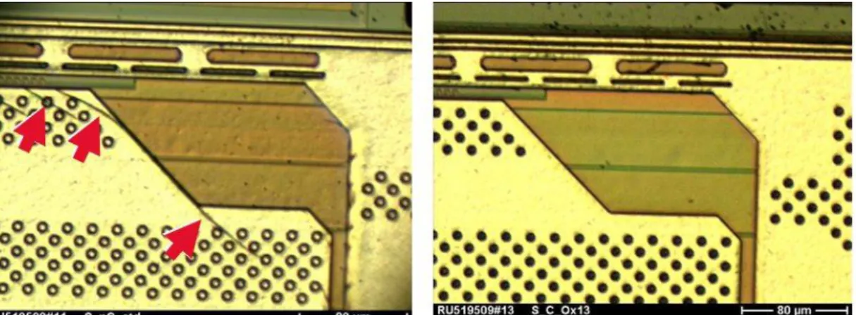
In most cases the metal on the chip frontside is only 5µm thick or even thinner down to 3µm in power semiconductors. Besides this, the topology of the metallisation is defined by the structure underneath the metal. Figure 14 shows a comparison of three different, MOSFET devices. The sealing of the contact hole and the robustness for wirebonding is defined by the edge coverage of the aluminium which is defined by the contact hole geometry and sputter parameters for the aluminium deposition.
Figure 14: Comparison of contact holes in terms of metallization sealing. New technology platforms show excellent edge covering of the metallization.
The sealing of the chip towards ambient conditions is important to prevent corrosion and penetrating of ions into the semiconductor. After contact hole metal coverage optimization also the wirebonding processes have been adjusted in order to prevent further damage of the chip. From assembly side this issue was solved by a new generation of wirebonding parameters and by installing a new process control to make sure that the bond process results remains stable. In order to trace cracks in the frontside metallisation after wirebonding a reactive-ion-etch (RIE) analysis was established on sample base which decorates any cracks into the underneath Si oxide. Figure 15 shows an example of a 50µm Al wirebond with a very high penetration into the Al metallisation of the chip.
For power devices mainly Al wirebonding is applied as the interconnects on chip (Al/Al) and on lead (Al/NiP) are known to be metallurgically reliable up to 175°C and offer high current interconnects for MOSFET devices, therefore the focus in this work is on devices with Al wirebonding technology.
Recently in the last decade also Cu wire is used for power devices offering higher conductivity. In addition new semiconductor chip technologies are built with a Cu metallisation instead of the Al, using a Cu wire to directly bond on this Cu metallisation has the advantage of having the same metal for both partners and therefore no unfavoured metallurgical transformations.
Figure 15 : Example of an Al interconnect with too strong bonding parameters leading to a high penetration depth and damage of the chip metallisation. The blue line
indicates the crack direction.1 Adhesion promoter
Throughout the different fatigue mechanisms which can be found in a power semiconductor device the primary defect in most cases is delamination of the molding compound. In a package the metal to molding compound interface is the dominating one and is present on all critical positions like at the chip surface, around the chip, on the solder and around the bondwires. Out of the learning of the different failure mechanisms it was claimed to have an adhesion promoter which covers the full device surface in order not to exclude any position in this system from proper adhesion. This claim consequently means application of the adhesion promoter just before molding process in order to cover all surfaces and therefore prevent the formation of weak interfaces. Strong adhesion on all interfaces minimizes internal friction and plastic deformation within the whole device and is therefore minimizing secondary fatigue mechanisms, as for example shown in figure 16 for the chip frontside. With a thermomechanical stress of up to 2000 temperature cycles (-55°C until 150°C) no shift of metal lines can be found in this example of a MOSFET device in a TO263 package.
1 : Investigation done by Khalil Hosseini as an example of an Al wire bond interconnect
Robust Passivation in Robust Package
Konsequences of a Robust Product with full adhesion A: No delamination on lead & chip after TC2000 B: No electrical failures up to TC2000;
C: No shifted edgestructure on chip after TC2000
TC1000 TC2000
Strong delamination and shifted edgestructure during TC in non-robust
product.
Robust Package
Robust SFET2
Figure 16: Reliability results after 2000 TC (-55 °c to 150 °C) within a TO263-3 package with a 30mm² MOSFET chip. Ultrasonic microscopy images show no delamination after this stress and this corresponds with metal lines which are still in good order (left). In the non-robust product (right) without A2 strong shift of the metal lines is seen.
On the other hand applying the adhesion promoter in assembly requires effort of applying a specific layer on the device within an assembly line under clean room conditions. Choosing the suitable candidate of adhesion promoter and developing a manufacturing process for mass production was one of the challenges of this work.
Basically there are several adhesion promoters known which can mainly be categorized into two sections:
a. Promoters acting on molecular level.
b. Promoters acting on mechanical level.
For example primers are acting on molecular level and require a proper preparation of the surface chemistry to be able to form the relevant chemical bonds. In many cases these reactions are very specific and limited to certain metal oxides and metals. The deposition of that species can be done by dipping or spraying. The surface preparation has to be specifically generating a surface chemistry which fits to the functional groups of the primer. Figure 17 shows a molecule of a benzotriazole-derivative which is designed specifically to fit to Cu surfaces due to the triazo-group. The aromatic hydroxyl-function is reactive towards the oxiran function of common epoxy resins of
Figure 17: Example of a primer working on molecular level. In this case these
triazolium type system are dedicated to Cu surfaces and the hydroxyl group is linking to oxiranes of epoxy resins.
The second category are adhesion promoters acting on mechanical level. Mechanical adhesion promoters are mainly adhering through mechanical interlocking. There are always also chemical or physical forces working like van-der-Waals forces or hydrogen bridges, but those are not the dominating forces and therefore the surface chemistry compatibility to the resin is not that crucial as with molecular adhesion promoters. On the other hand mechanical adhesion promoters are performing only effectively if the morphology is fitting to the used polymer. In the section 3 identification of suitable candidates will be deeper discussed, Figure 27 shows two examples of mechanical adhesion promoters with their specific pore size.
Encapsulation - Molding compounds
Regarding reliability of molding compounds it was described above already that there are a couple of resin systems available to manufacture molding compounds with high Tg
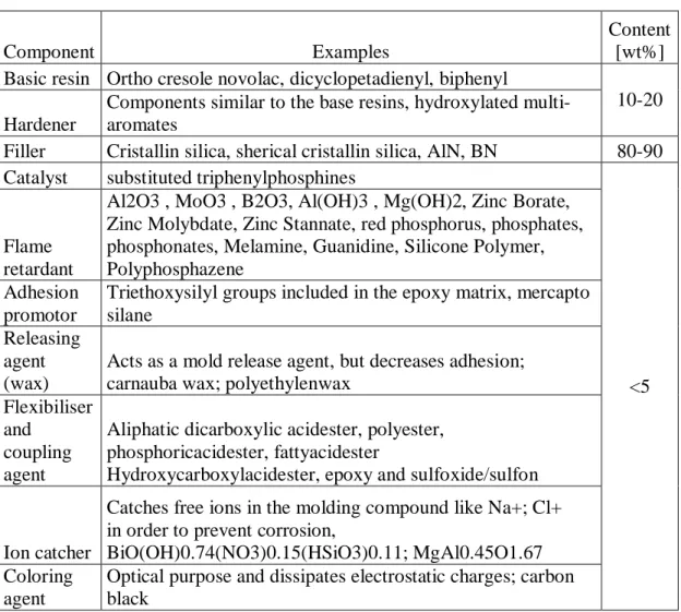
and with specific properties. Target properties achieve minimized stress level for the package, an optimum processability during molding, and full compatibility to all surfaces. There are many orders of freedom in designing a molding compound since there are more than 10 different ingredients in modern molding compounds which have specific chemical and geometrical properties like the filler size, shape and filler material. Table 2 shows an overview of components required for the formulation of a molding compound. The composition of this material formulation defines how the material behaves in the manufacturing processes and in the product.
Component Examples
Content [wt%]
Basic resin Ortho cresole novolac, dicyclopetadienyl, biphenyl
10-20 Hardener
Components similar to the base resins, hydroxylated multi- aromates
Filler Cristallin silica, sherical cristallin silica, AlN, BN 80-90 Catalyst substituted triphenylphosphines
<5 Flame
retardant
Al2O3 , MoO3 , B2O3, Al(OH)3 , Mg(OH)2, Zinc Borate, Zinc Molybdate, Zinc Stannate, red phosphorus, phosphates, phosphonates, Melamine, Guanidine, Silicone Polymer, Polyphosphazene
Adhesion promotor
Triethoxysilyl groups included in the epoxy matrix, mercapto silane
Releasing agent (wax)
Acts as a mold release agent, but decreases adhesion;
carnauba wax; polyethylenwax Flexibiliser
and coupling agent
Aliphatic dicarboxylic acidester, polyester, phosphoricacidester, fattyacidester
Hydroxycarboxylacidester, epoxy and sulfoxide/sulfon
Ion catcher
Catches free ions in the molding compound like Na+; Cl+
in order to prevent corrosion,
BiO(OH)0.74(NO3)0.15(HSiO3)0.11; MgAl0.45O1.67 Coloring
agent
Optical purpose and dissipates electrostatic charges; carbon black
Table 2 : Overview on different substances used for molding compound formulation.
The molding process has to be fast due to high equipment investment, so the polymerisation kinetics defined by the resin, hardener and catalyst is optimized by the supplier of the molding compound. On the other hand during the injection of the material into the moldtool the viscosity has to be limited, the viscosity increase of the liquid resin needs a specific delay until the full injection is over and then a fast hardening is required. Especially for packages with nanoporous adhesion promoters the selection of suitable polymerisation kinetics is important to be able to fully penetrate into the adhesion promoter layer.
Finally, after resin hardening the product needs to be released from the moldtool. Due to the volume shrinkage of the epoxy matrix during hardening this is no big problem for molding compounds with low volume fraction of fillers as the overall shrinkage is quite
CTE of the molding compound is defined by the mixture of resin with a very high CTE and the filler particles with a quite low CTE.
Besides processability there are some reliability aspects to consider for choosing molding compounds.
In order to reduce the stress to the chip surfaces molding compounds with advanced filler contents have been developed. In order to adapt the average CTE of the molding compound to silicon filler loading, type and shape has been optimized. There are materials which reach CTE very close the CTE of silicon (Example: Shinetsu KMC2110-7G: α1 = 6*10-6 K-1 (T<TG); α2 = 36*10-6 K-1 (T<TG); Silicon: αSi = 2,9*10-6 K-1). There are other factors arising with those low CTE materials especially with semiconductors manufactured with aluminium metallisation. The CTE of aluminium (αAl = 23*10-6 K-1) is much higher compared to the CTE of those molding compounds which leads to an increase of thermomechanical stress towards the aluminium metallisation.
1.6 Focus of this work
Several process steps and materials have to be optimized to get a highly reliable power semiconductor device. One important understanding out of the fatigue mechanisms in such a device is, that delamination of the molding compound is responsible for several fatigue mechanisms. Solving this adhesion problem is the crucial element to get a robust product. There are many approaches to increase adhesion. The focus of this work is the identification of a suitable adhesionpromoter and the development of this candidate up to mass production. The target with this technology was set to achieve 260°C PCB solder heat resistance at MSL1 (85°C/85%rel.hum) and TC2000 (-55 to 150°C) with full adhesion and stable electrical parameters over these stress tests.
The second focus of this work is the surface design of copper surfaces with organic molecules. This is applied for soldering and for bonding of Cu wire to the Cu metallisation of power semiconductor chips. To prevent oxidation of the Cu surfaces different passivation concepts have been worked out to enable the broad usage of this metal for power semiconductor devices.
2 Analytical and experimental methods
In the following sections the discussion of the experimental results will be made based on various analytical and experimental methods. Therefore in this chapter these methods are briefly described first. All experimental and analytical results that are being discussed are structured in a similar way using a specific number for the individual experiment, such as er265, and for each experiment specific sub-experiments are named as groups with specific numbers or characters, such as er265-1 or er265-A. The experimental matrices with the specific group numbering are given in the various experimental sections.
2.1 Field emission scanning electron microscope (FESEM): Surface morphology
Most of the analysis of deposited layers in terms of surface topology has been done with field emission scanning electron microscopy (FESEM). The basic principal of SEM imaging is the scanning of a surface with a focused primary electron beam (EB) consisting of a energy of up to 15keV. The generation of the EB within a FESEM is done with a cold field emission gun which is for example a tungsten needle within a very high electric field E > 109 V*m-1. Under these conditions, in a high vacuum of about 10-7 mbar, electrons are emitted into the vacuum by tunnelling through the tungsten oxide barrier of the tungsten cathode. They are then accelerated by a voltage of 1-50kV between cathode and anode forming a very fine EB which offers a resolution for example of 0.4nm at an acceleration voltage of 30kV and of 1.2nm at 1kV [9]. A similar generation of the EB is done with a Schottky field emission source which offers the advantage of higher beam current while still maintaining good resolutions for example of 1.0 nm at an acceleration voltage of 15kV and 1.6nm at 1kV [10].
During the collision of the EB with the surface various interactions with the sample material happen as illustrated in figure 18. For FESEM mainly the signal of the low energy secondary electrons (SE) generated directly by the EB is detected. Depending on the angle of the sample, the amount of SE is varying and the signal variation during scanning of the surface by the electron beam enables the generation of a sharp 3-
dimensional image of the topology of the surface. SEs are released out of a depth of the first 10nm of the sample.
In addition modern FESEM equipment has a back scattering electron (BSE) detector.
BSE are generated through elastic scattering of the primary electrons with the atomic nuclei of the sample and due to the elastic scattering they do not loose very much energy in comparison to the primary electron beam. Therefore, the BSE can come out of a depth of several hundred nanometres. In addition, the yield of BSE is strongly dependent on the atomic number, which is related to the atomic mass of the material.
Therefore the BSE signal offers a material contrast which gives an indication of the chemical composition of the sample [11].
SE (secondary electrons)
BSE (back scattering electrons) AE (Auger electrons) characteristic X-ray
Bremsstrahlung CL (cathodoluminescence)
Primary electron beam
sample
Figure 18: Interactions between an electron beam with a material.
An additional interaction between EB and the samples is generating Auger electrons explained later in chapter "2.7 Auger electron spectroscopy (AES)". Furthermore cathodoluminescence is an emission of light in the visible range of the electromagnetic spectrum (λ=400-700nm) generated by the primary electron beam, but the information based on this interaction is of less importance for FESEM and only important for specific semiconducting materials in analysis of for example doping concentrations [11]. Finally, emission of radiation in the lower wave length region as characteristic X- ray or as Bremsstrahlung is observed which is not discussed in this section. However, the former one is important for energy dispersive X-ray (EDX) analysis that is discussed in chapter "2.2 Energy dispersive x-ray spectroscopy (EDX)".
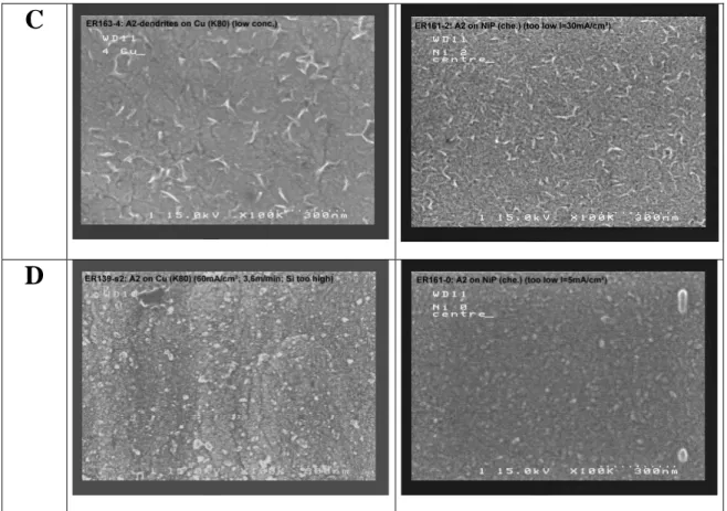
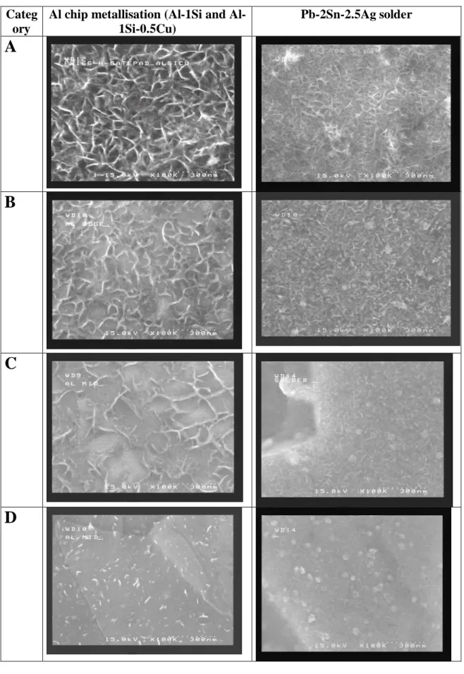
Specifically for the sponge structure of the A2-layer FESEM analysis was mostly done at 15kV acceleration voltage and a magnification of 100k. Since the most important property of the A2-layer is the surface morphology, enabling a mechanical interlocking function to the molding compound, the surface analysis with FESEM became a major part of the characterization of the deposition process together with the adhesion tape test described in chapter "2.5 Tape adhesion test". For the purpose of characterizing various morphologies on the various surfaces, a morphology catalog was defined based on FESEM results to assess the quality of the various deposits in 4 categories which are shown in table 3 for Cu and NiP and in table 4 for the Al chip metallisations and the solder surface.
Morphology catalogue of A2-coating for different adhesion performances Categ
ory
Cu surface NiP surface
A
B
C
D
Table 3: FESEM based catalogue of various A2 dendrite morphologies on Cu and NiP surfaces rated A to D.
Categ ory
Al chip metallisation (Al-1Si and Al- 1Si-0.5Cu)
Pb-2Sn-2.5Ag solder
A
B
C
D
Table 4: FESEM based catalogue of various A2 dendrite morphologies on Al chip
For each substrate having the A2-layer, the categories A-D were defined with the following observations in the FESEM with 100k magnification:
Category A: Dense, homogenous sponge structure
Category B: Dense sponge structure with single spots without a A2 layer where the flat substrate is visible.
Category C: Sponge structure with bigger areas in between where the flat substrate is visible.
Category D: None or only single needles can be observed, mostly the flat substrate morphology is present.
These categories were used in the respective experiments to distinguish between the results of the specific process conditions.
2.2 Energy dispersive x-ray spectroscopy (EDX)
In the previous chapter the interaction of an electron beam with a material was described and two important interactions leading to the emission of radiation with lower wavelength (λ ≤ 400nm) given. For the case of Bremsstrahlung a continuous spectrum is emitted, in addition x-rays with characteristic wavelength for the specific material are emitted. The latter one is generated through the excitation of an atom via x-ray or via the electrons of an electron beam. Excitation means the striking out of an electron from the orbital of an atom of the specific material which leads to a shift of electrons with higher energy from higher orbitals within the atom shell towards lower energy orbitals.
The energy difference for this shift is equal to a characteristic wave length for a specific atom for a specific line which is given by equation (1). In this equation h is the Planck constant (6.626*10-34 J∙s), ν is the frequency of the radiation (s-1), c is the light speed (2.997∙108 m∙s-1) and λ is the wavelength (nm).
h c h
E (1)
For example the interaction of an electron beam with Cu atoms leads to the following characteristic wavelengths which will be emitted from the sample: λK,α1,Cu = 1.5406 *
10-10 m , λK,α2,Cu = 1.5444 * 10-10 m, λK,β1,Cu = 1.3922 * 10-10 m, λL,α1,Cu = 15.286 * 10-
10 m, λL,β1,Cu = 13.053 * 10-10 m [2]. In energy dispersive x-ray spectroscopy (EDX) the characteristic energies are measured to detect the elements within the sample, the detectors are mostly combined with a SEM (scanning electron microscopy), FESEM (field emission scanning electron microscopy) or a TEM (transmission electron microscope). The characteristic radiation is generated within a depth of several micrometres depending on acceleration voltage and on the sample material. Hence, as a surface analysis tool EDX has limited application. More details are described for example from Oettel [11] and from Martin [15].
2.3 Transmission electron microscopy (TEM)
In contrast to SEM described above TEM requires very thin samples that are in the thickness range of 10 to 100nm. Preparation of the sample requires higher effort as the material has to be first encapsulated in epoxy and then thinned mechanically and polished to the necessary thickness with an ion milling equipment. Ion milling is done with 1-5keV Ar+ low energy ions at low incident angle of <5° on mechanically cut foils that consist of the sample embedded in a resin.
Samples that are chemically and mechanically more stable, like materials from semiconductor devices, often are prepared through generation of a lamella via focus ion beam cutting (FIB)1.
Then the sample is placed in a vacuum chamber and percolated from an electron beam.
The electron source used for TEM is working similarly as with FESEM/EDX using energies of 80 to 400keV. Due to the low thickness of the sample the electron beam intensity is decreasing only to some extent moving through the sample and the remaining primary beam intensity is detected. Depending on the material the electron
1 : Focused ion beam method (FIB) uses Gallium ion beams (30keV) to cut into the surface and sputter material off the surface. A sharp cut edge is forming at the cutting crater. With this method thin slices for TEM can be cut out of the bulk material and mounted onto the TEM holder. The final sample thickness of
beam is scattered. Via special apertures the unscattered electrons are collected in the primary beam direction, the intensity detected depends on the atomic number of the elements in the samples. Similar to SEM an area in the x/y plane is scanned and a contrast picture can be obtained. Thick areas of the samples and areas with heavy atoms will appear dark and a bright contrast is obtained with thinner sample areas and material consisting of lighter atoms.
In addition with specific detector positions the back scattered electrons and the electrons that are undergoing diffraction are collected. More complex information can be gained concerning the crystallographic properties in the specific sample position
Besides the detection of electron intensities the combination with x-ray detectors is common enabling the collection of EDX spectra for elemental analysis as with SEM/EDX. For deeper information on TEM and sample preparation see Lee [12] who gives a brief review. An overview on methods for local chemical analysis of materials is given by Martin [15] and Schumann and Oettel [11].
2.4 Button shear test
Copper plates with the NiP plating (A = 2 x 10 cm²) and the deposited A2 structure are subjected to a molding press (LHMS-28M equipment from Lauffer GmbH & Co KG) where five molding compound buttons in one row are moulded onto the plates via a dedicated molding tool. These molding compound buttons have exactly the same size as the molding compound of a TO263-3 device (Area = 9.25 x 10 mm²; height = 3.1mm).
After molding, the plates are further processed with post molding curing to get similar properties of the polymerized epoxy as within the real product. After their manufacturing, the molding buttons can be destructively sheared off in parallel to the Cu plate with a shear tester measuring the respective shear force at breakage of the buttons from the plate. This test is done for specific samples after specific stress test on the plate such as MSL1/260°C soldering or temperature cycling (TC) to simulate degradation effects that may result in interface adhesion deterioration which then are measured by the shear tester.