June 15, 2011
Abstract
A computer system consisting of a soft processor, a small data and instruction memory, input from swiches, output to LEDs, a serial interface for communication with the PC and a debug interface will be configured out of IP cores and programmed in C.
1 Hardware Design
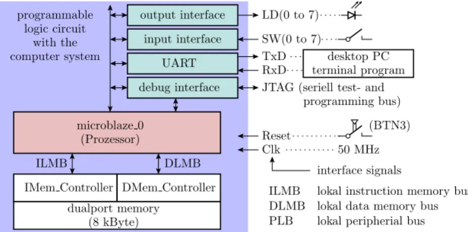
An embedded computer system consists of a processor, memory and peripherial interfaces for communication with its environment. Figure 1 shows the block diagram of the computer system to be designed. The core is a 32-bit RISC processor, type MicroBlaze. That is a processor especially optimized for the implementation in programmable logical circuits (FPGAs). The processor is connected to the data bus (DLMB), the instruction bus (ILMB) and the pe- ripherial bus (PLB). The data and the instruction bus are each connected via a memory controller to one of the ports of a dual port memory. To the peripherial bus (PLB)
Clk
interface signals 50 MHz
(BTN3) Reset
ILMBDLMB PLB
lokal instruction memory bus lokal data memory bus lokal peripherial bus RxDTxD
SW(0 to 7) LD(0 to 7)
terminal programdesktop PC JTAG (seriell test- and
programming bus) microblaze 0
dualport memory (8 kByte)
ILMB DLMB
UART
(Prozessor)
IMem Controller DMem Controller programmable
logic circuit with the computer system
output interface input interface
debug interface
Figure 1: The computer system to be designed
1
• a parallel inteface to drive 8 LEDs,
• a parallel interface to input data from 8 switches,
• a serial interface for communication with the desktop PC and
• and a special debug interface for runnung programms in step mode, seting break points etc..
are connected. An embedded computer system does not have a keyboard, a hard disk or a monitor. The program will be downloaded into the programmable cir- cuit in the same way as the hardware configuration via the JTAG bus. The user input and output is carried out via the serial interface and the communi- cation with the debugger via the JTAG. The reset button is »BTN3«. Via the 8 switches a byte can be entered and via the 8 LEDs the value of a single byte can be displayyed. The system clock is 50 MHz and will be provided by IC4 at the bottom side of the test board.
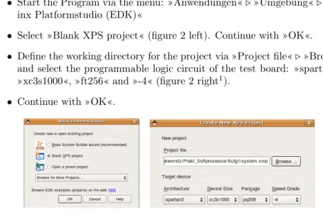
1.1 Create a new Project
• Start the Program via the menu: »Anwendungen«.»Umgebung«.»Xil- inx Platformstudio (EDK)«
• Select »Blank XPS project« (figure 2 left). Continue with »OK«.
• Define the working directory for the project via »Project file«.»Browse«
and select the programmable logic circuit of the test board: »spartan3«,
»xc3s1000«, »ft256« and »-4« (figure 2 right1).
• Continue with »OK«.
Figure 2: Create a new project
1Attention input bug: you have to click at all menu items, even if the displayed values don’t have to be changed.
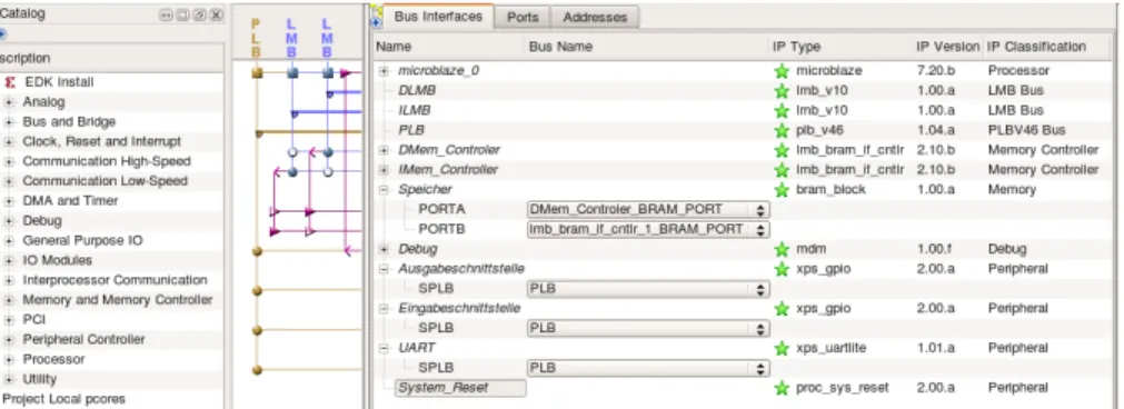
Figure 3: Selecting the functional blocks from the IP catalog
1.2 Selection, Configuration and Connection of the IP- Cores
2At the user interface beneath the left window the tab »IP Catalog« has to be selected. The required IP-cores have to be draged with the mouse to the right side. In figure 3 it has already been done. The following table summerizes for all 10 functional blocks the category, the original name and how they have to be renamed in correspondece to figure 1.
category circuit type to rename in
Prozessor MicroBlaze microblaze_0∗1
Bus and Bridge Local Memory Bus (LMB) DLMB
Bus and Bridge Local Memory Bus (LMB) ILMB
Bus and Bridge Processor Local Bus (plb_v46) PLB Memory and Memory Contr. LMB BRAM Controller IMem_Controller Memory and Memory Contr. LMB BRAM Controller DMem_Controller
Memory and Memory Contr. Block RAM (BRAM) Speicher
Debug MicroBlaze Debug Module (MDM) Debug
General Purpose IO XPS General Purpose IO Ausgabeschnittstelle∗2 General Purpose IO XPS General Purpose IO Eingabeschnittstelle∗3
Communication Low Speed XPS UART (Lite) UART
Clock, Reset and Interrupt Processor System Reset Module System_Reset
∗1The name of the processor should not be changed. Otherwiese there may arise difficuilt to understand problems within the software developement system SDK, e.g. using capitalized char- acters causes confusion with the search pathes of design objects; ∗2 output interface; ∗3 output interface;
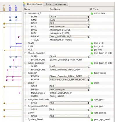
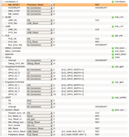
For renaming the original name has to be selected with the left mouse button and overwritten. Next the bus connections have to be arranged. Of the processor the data bus (DLMB), the instruction bus (ILMB) and the peripherial bus (DPLB) have to be connected with system busses as shown in figure 4 by clicking
2IP-Cores are pre-designed, configurable circuit descriptions. The acronym IP stands for
»intellectual property«.
Figure 4: Renaming and bus connections
at the cross points at the graphic. Each memory controller has to be linked to the memory bus, each port of the dual port memory with the red bus connector of the memory controllers and the three interface circuits with the peripherial bus (PLB). The debug interface hase to be connected with peripherial bus and a special debug port of the processor.
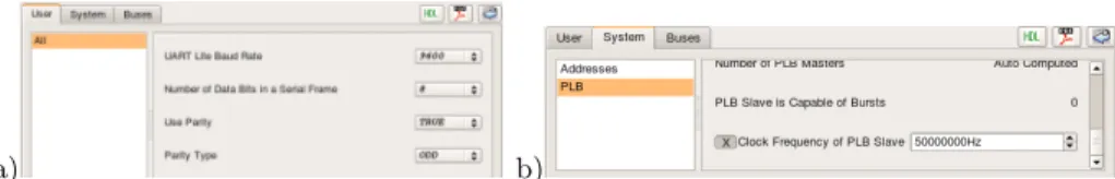
The peripherial interfaces have to be configured. For the output interface for »Channel 1«, tab »User« data width has to be reduced downto 8 (figure 5 a). In addition »Channel 1 Data Default Value« should be changed so that after initialization four LEDs are on and four LEDs are off. As shown in figure
a) b)
Figure 5: Configuration a) output interface b) input interface
5 b for the input interface the data width should be also reduced downto eight and for »Channel 1« the flag »Input Only« has to be set to true.
For the UART (universal asyncronous receiver transmitter) the setting in the menu »User« in figure 6 a can be kept or changed. It is only important that the setting are conform with those in the terminal program later used for communication with the PC. In menu »System, PLB« figure 6 b, clock frequency has to be reduced to »50000000Hz« (50 MHz)3.
a) b)
Figure 6: UART settings a) baud rate und transmission parameters b) clock frequency
The configuration of the debug port can kept unchanged and for the proces- sor via »Config IP« tab »Debug«»Enable Microblaze Debug Module Interface«
has to be selected. Otherwise during program start of SDK an error will arise.
1.3 External Connections
Change to the view »Ports (figure 7). The circuit in figure 1 has a clock in- put (Clk), an initialization input (Reset), a serial input (RxD), a serial output (TxD), an 8-bit output vector »LD« to the LEDs and an 8-bit input vector
»SW« from the switches. First by button »Add External Port« top right for each interface signal a delaration line has to be added and than to be adjusted.
The names in column »External Ports« must be the same as in the constraint file. In column »Net« the internal name has to be declared, normally the same as for the port. In column »Direction« »I« means »input« and »O« means
»output«. For both bitvectors in column »Range« the index range should be specifyed ascending as the data. In column »Class« clock and initialization sig- nals has to be labeled as special signals. Next the external ports are connected to the computer components by entering there names in corresponding menus.
3First click at the »X«. Afterward the frequency value can be edited.
Figure 7: External Ports
To the data, instruction and peripherial bus the clock and the initialisation sig- nal, preprocessed by the system reset unit are connected. The output port has to be connected to the LEDs, the input port to the switches and the UART with serial signals »RxD« and »TxD«. The internal reset signal, provided by the debug interface has to be connected to the corresponding input of the sys- tem reset unit. The »Slowest_sync_clk« for sampling and time alignment is the clock »Clk« and the external reset signal is reset »Reset«. The unused ad- ditional reset input »Aux_Reset_In« has to be connected to »net_gnd« and the unused input »Dcm_locked«4 to »net_vcc«.
1.4 Define the Adress Ranges
In tab »Adresses« to the data memory controller, the instruction memory con- troller, the parallel, the serial and the debug interface adress ranges has to be defined (figure 9). With the button »Generate Adresses« default values are
4Using a DCM this signal delays the deactivation of the internal reset signal until the delay loop is locked.
Figure 8: Connecting the external Ports with the System Components
generated. The smallest allowed size for block memories is 8 kByte. The adress ranges for instructions and data should be the same. The peripherial units need non-overlapping adress ranges. For the parallel interfaces the smalles selectable
»Size« value is big enough. For the UART a reservation of an adress range smaller then 2 kByte causes malfunctions. The default values of 64 kByte per device can also be retained. For the total adress range is232 Byte, so that the oversized device adress ranges will not cause a shortage.
Figure 9: Defining adress ranges
1.5 Creating the Constraint File
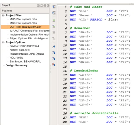
As in the designs with »Xilinx-ISE« the (user)constraintfile (UCF) assignes package pins to interface signals, timing and other constraints. It is important to specify the clock period, so that the synthesis can check, whether the circuit is fast enough. The constraint file will be selected via the tab »Project Files«
and select »UCF File data/system.ucf«. Figure 10 shows the required entries for the example design.
1.6 Finishing the Hardware Design
The software design should be carried out by the »eclipse« based development environment »SDK«:
• »Project«.»Export Hardware Design to SDK ...«
• »Export and Launch SDK«
The synthesis, placement and wiring lasts several minutes. After finishing sucessfully a sub-directory »SDK/SDK_Export/hw/« is ceated, containing all hardware specific information including the bit-file for programming, software driver for peripherial components etc. SDK can also be launched directly from the menu bar under linux by
• »Anwendungen«. »Umgebung«. »Xilinx Plattformstudio (SDK)«
After launch the working directory has to be changed to »SDK/SDK_Work- space« of the current »EDK« project, where »SDK« will find the file ».meta- data« of the project.
Figure 10: : Required entries in the constraint file
2 Software Development under SDK
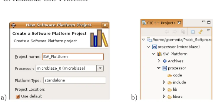
Create a software plattform by:
• »File« .»New« . »Software Plattform ...«. »Add Software Application Project ...«
As in figure 11 a, the software plattform should be named »SW_Plattform«.
During finishing in the sub-directory »processor/include« of the software plat- tform the hardware specific libraries for software development are created (figure 11 b ).
After creating the software plattform a project has to be created:
• »File« .»New« . »New Managed Make C Application Project« .select a name, select »Empty Application«.continue clicking until finishing In figure 12 left the name of the new project is »Einfuehrung« (engl. introduc- tion). Within the project a programming file has to be created:
• »File« . »New« . »Source File« . select a name ending with ».c« and finish
a) b)
Figure 11: a) Creating a software plattform b) Object tree of the software plattform
Figure 12: : Project example with a programming fault
The newly created file, in the example »Test1.c«, will, as shown in figure 12 left, be stored in the project directory. Open it by dopple click to edit the programm. By storing, the programm will be compiled automaticly. Detected syntax faults are displayed in the source code. In figure 12 line 11 contains a fault – the »+« in front of »while« – that has to be removed before an executabel programm will be produced.
2.1 The programming Example
The example programm in figure 12 starts with the include-instructions:
#include "xparameters.h"
#include "xgpio_l.h"
#include "xuartlite_l.h"
to import the required constants, makros and subroutines to controll the pe- ripherial interfaces. The project uses from »xparameters.h« the base adresses of the input and output interfaces
XPAR_AUSGABESCHNITTSTELLE_BASEADDR XPAR_EINGABESCHNITTSTELLE_BASEADDR XPAR_UART_BASEADDR
from »xgpio_l.h« the functions and macros for parallel input and output XGpio_mWriteReg(BaseAddress, RegOffset, Data)
XGpio_mReadReg(BaseAddress, RegOffset)
and from »xurartlite_l.h« the functions and macros for serial input and output XUartLite_RecvByte(XPAR_UART_BASEADDR)
XUartLite_SendByte(XPAR_UART_BASEADDR, data)
The name of the main program that takes control after starting the embedded system is in »c« always »main«. In the example at the begin of the programm the string constant »Hallo Welt\r\n« is created in the instruction memory and a pointer to the begin of the string and a variable to store a single character are declared:
int main() {
char *str = "Hallo Welt\r\n";
char data;
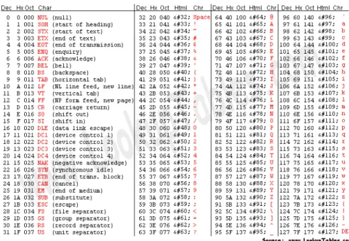
A string in »c« allways ends with a true »0«. The two control characters »\r\n«
have the values »0c0D« and »0x0A« (see ASCII table in figure 13). All up the string »Hallo Welt\r\n« corresponds to the number sequence »0x48 0x61 0x6c 0x6c 0x6F 0x20 0x57 0x65 0x6c 0x74 0x0D 0x0A 00«5. The following while loop sends characters and increases the pointer untill the character value is zero. In this way the whole character sequence including line feed is sended to the PC:
while (*str != 0) {
XUartLite_SendByte(XPAR_UART_BASEADDR, *str);
str++;
}
In each run of the following infinite loop the program waits on a byte from the serial interface, displays the byte value on the LEDs, sends the byte back to the PC, reads a byte value from the switches and sends it also to the PC. To return the space character between two received characters, the switches must be set to 0x20:
5Please check it with the ASCII table in figure 13 an later during step operation (pausing execution after each instruction).
Figure 13: ASCII table for translation between characters and character values
while (1) {
data = XUartLite_RecvByte(XPAR_UART_BASEADDR);
XGpio_mWriteReg(XPAR_AUSGABESCHNITTSTELLE_BASEADDR, 0, data);
XUartLite_SendByte(XPAR_UART_BASEADDR, data);
data = XGpio_mReadReg(XPAR_EINGABESCHNITTSTELLE_BASEADDR, 0);
XUartLite_SendByte(XPAR_UART_BASEADDR, data);
} }
2.2 Program Test
Before testing the program
• connect the test board to the power supply and the programming cable and load the hardware configuration in the programmable logic circuit by
• »Tools«.»Program FPGA«. »Save and Program«
Bevore starting the program it is also usefull to start the serial port terminal on the PC:
• »Linux Menu bar«.»Anwendungen« . »Zubehör«.»Serial port termi- nal«
Within the terminal program adapt the port settings via:
• »Configuration«. »Port«
The port settings must be the same as for the soft processor, in the example speed »9600«, parity »odd«, bits »8«, stopbits »1« and flow control »none«.
Connecting the testboard to the PC via a normal serial cable the port name is generally »/dev/ttyS0«. Using an USB to serial adapter look before and after plugging in the cable what the newly created device port is. If no transmission can be established, the wrong port may be selected or an other program has locked the port. In the last case the other program has to be closed and the serial port monitor started again. The reason of eye-catching data corruptions is generally wrong baud rate setting. Alternatively also a wrong clock frequency of the UART in figure 6 b may be the source of the malfunction.
After a successful download and the start of the serial port monitor start the program with
• »Run«. »Run ...«. ... .select »Debug/Einfuehrung.elf«
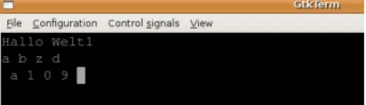
After start and pushing the reset button »BTN3« the program sends to the serial port terminal the text »Hallo Welt«, a newline and a carriage return, waits in each iteration on a character from the PC, displays the character value on the LEDs, returns the received character to the PC, reads the 8-bit value from the switches and sends it as a character also to the PC. Figure 14 shows as an example the monitor output for the input sequence »abzd<Enter>a109«
and switch setting 0x20 (space character).
Figure 14: Example of the test output displayed by the serial port terminal Transmitter and receiver of UART, each have an 8 character buffer, witch by chance may be filled with characters. This may cause that the program may receive or transmit unexpected characters after (re-) starting the program.
2.3 Debugger
As in section before, before starting the debugger the hardware configuration has to be downloaded and the serial port terminal on the PC has to be started.
The debugger is started with :
• »Run«. »Debug ...«.... . select »Debug/Einfuehrung.elf«.»Debug«
A usual way for a systematic initial test of a program is to run it in jog operation or little pieces. For this the program will be stopped after each instruction to check the intermediate data. The debugger has the following mechanism to stop a program:
• »Run« . »Step Into«: stops after the next instruction, in case of a sub- routine call after the first instruction of the subroutine.
• »Run« .»Step Over«: stops after the next instruction, in case of a sub- routine call after returning from the subroutine.
• set a break point: »right mouse click before the line number«. »Toggle Breakpoint«
• start/continue programm (»Run«.»Resume«): stops at the next break- point.
For break points also a condition and an ignore count can be added, that must be true or counted down to zero, respectively, to interrupt the program. Though, the program may pass break points in loops several time before stopping. To visualize the value of a variable during a halt of the program place the mouse pointer over the variable. In figure 14 in the yellow window, pointer (address value) »str« and the string constant starting at this address are displayed. Dur- ing the debugging of the example program keep in mind, that the function
»XUartLite_RecByte(...)« within the inner loop waits always on a character from the PC. Without this input or without running the serial port terminal the debugger waits eternally.
3 Exercises
Aufgabe 1.1: EDK-Referenzentwurf
Do the hardware design in the described ways with EDK.
Aufgabe 1.2: SDK-Referenzentwurf
Export the hardware design to SDK and carry out the software design in the described ways with SDK.
1. First test the program with »run«.
2. Repeat the test with the debugger in step operation.
• Write down the value of the pointer »str« and the value it points to in each Iteration of the first while-loop.
• Set a break point in front oft the instruction that read the switches.
Check whether the program stops before or after the break point.
1 2 3 4 6 5 2
1 3
5 4
6
Step Into Step Over Resume
Variablen Wertes einer Adresse des Anzeige der Befehlsz¨ahler punkt
Unterbrechungs-
Figure 15: Program surface of the debugger
Aufgabe 1.3: Erstes eigenes Programm
Change the program so that the bytes received from the UART and displayed at the LEDs are processed in some way e.g. combined bitwise EXOR with the data read from the switches. Fill in the following tabular with test cases and carry out the tests.
character recieved by
the UART
character value
switch input LED-output
’a’ 0x43
’1’ 0x65
4 Questions for self-monitoring
• How long needs the transfer of the word »Hallo« with the UART-settings:
9600 baud, one start bit, eight data bits, one parity bit and one stop bit?
• Write your name, followed by a line feed as an ASCII-String.