The QPACE Supercomputer Applications of
Random Matrix Theory in Two-Colour
Quantum Chromodynamics
Dissertation
zur Erlangung des Doktorgrades der Naturwissenschaften (Dr. rer. nat.)
der Fakult¨at f¨ur Physik der Universit¨at Regensburg
vorgelegt von
Nils Meyer
aus Kempten im Allg¨au
Mai 2013
Datum des Promotionskolloquiums: 14.06.2016 Pr¨ufungsausschuss:
Vorsitzender: Prof. Dr. C. Strunk Erstgutachter: Prof. Dr. T. Wettig Zweitgutachter: Prof. Dr. G. Bali weiterer Pr¨ufer: Prof. Dr. F. Evers
F¨ ur Denise.
Contents
List of Figures v
List of Tables vii
List of Acronyms ix
Outline xiii
I The QPACE Supercomputer 1
1 Introduction 3
1.1 Supercomputers . . . 3
1.2 Contributions to QPACE . . . 5
2 Design Overview 7 2.1 Architecture . . . 7
2.2 Node-card . . . 9
2.3 Cooling . . . 10
2.4 Communication networks . . . 10
2.4.1 Torus network . . . 10
2.4.1.1 Characteristics . . . 10
2.4.1.2 Communication concept . . . 11
2.4.1.3 Partitioning . . . 12
2.4.2 Ethernet network . . . 13
2.4.3 Global signals network . . . 13
2.5 System setup . . . 14
2.5.1 Front-end system . . . 14
2.5.2 Ethernet networks . . . 14
2.6 Other system components . . . 15
2.6.1 Root-card . . . 15
2.6.2 Superroot-card . . . 17 i
3 The IBM Cell Broadband Engine 19
3.1 The Cell Broadband Engine and the supercomputer league . . . 19
3.2 PowerXCell 8i overview . . . 19
3.3 Lattice QCD on the Cell BE . . . 20
3.3.1 Performance model . . . 21
3.3.2 Lattice QCD kernel . . . 22
3.3.3 Data layout analysis . . . 22
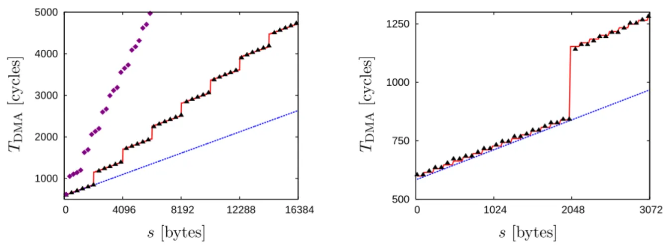
3.4 DMA transaction models . . . 24
3.4.1 Local Store to Local Store . . . 25
3.4.2 Local Store to main memory . . . 26
4 The QPACE Network Processor 29 4.1 FPGA technology . . . 29
4.2 Network processor overview . . . 30
4.3 Device Control Register bus . . . 32
4.3.1 Device tree topology . . . 33
4.3.2 Bus interface and protocol . . . 34
4.3.3 Master implementation . . . 36
4.3.4 Arbiter implementation . . . 37
4.3.5 Synchronous DCR interface implementation . . . 39
4.4 Inbound Write Controller . . . 41
4.4.1 Implementation . . . 43
4.4.2 State machine . . . 46
4.5 Universal Asynchronous Receiver Transmitter . . . 47
4.5.1 Implementation . . . 48
4.5.2 Register file and modes of operation . . . 50
5 System Verification and Software Tools 53 5.1 System tests . . . 53
5.2 Software tests . . . 54
5.3 Booting the node-cards: ncBoot . . . 55
5.3.1 Implementation . . . 55
5.3.2 Command line interface . . . 56
5.3.3 State machine . . . 57
5.4 QPACE Front-end Client . . . 57
5.4.1 Implementation . . . 58
5.4.2 Command line interface . . . 59
5.4.3 Error handling . . . 60
CONTENTS iii II Applications of Random Matrix Theory in Two-Colour Quantum Chro-
modynamics 63
6 Quantum Chromodynamics 65
6.1 Introduction . . . 65
6.2 Non-Abelian gauge theory . . . 66
6.3 Chiral symmetry . . . 68
6.3.1 Introduction . . . 68
6.3.2 Gauge group SU(3) . . . 69
6.3.3 Gauge group SU(2) . . . 69
6.3.4 Chiral condensate . . . 70
6.4 Low-energy effective theory . . . 71
6.4.1 Motivation . . . 71
6.4.2 Lagrangian of the effective theory . . . 72
6.4.3 Non-zero baryon chemical potential . . . 73
6.5 Lattice QCD . . . 74
6.6 Fermions on the lattice . . . 76
6.6.1 Wilson-Dirac operator . . . 76
6.6.2 Lattice chiral symmetry . . . 78
6.6.3 Overlap operator . . . 81
6.7 Chemical potential on the lattice . . . 82
7 Random Matrix Theory 85 7.1 Introduction . . . 85
7.2 Hermitian chiral random matrix theory . . . 86
7.3 Non-Hermitian chiral random matrix theory . . . 89
8 Evaluation and Results 95 8.1 Two-colour QCD at zero chemical potential . . . 95
8.1.1 Choice of the Wilson mass . . . 95
8.1.2 Analysis of the distribution of the lowest-lying eigenvalue . . . 98
8.1.3 Analysis of the spectral density . . . 99
8.2 Two-colour QCD at non-zero chemical potential . . . 107
8.2.1 Spectrum of the overlap operator . . . 107
8.2.2 Analysis of the spectral density . . . 109
9 Summary 117 9.1 QPACE . . . 117
9.2 Lattice simulations of two-colour QCD . . . 117
Appendix 119
A QPACE Addendum 119
A.1 Sources . . . 119
A.2 DCR memory map . . . 120
A.3 witchlib API . . . 122
A.4 QFC full reference . . . 124
A.4.1 PSU specific actions . . . 124
A.4.2 Node-card specific actions . . . 125
A.4.2.1 Get mode . . . 125
A.4.2.2 Set mode . . . 126
A.4.2.3 Power mode . . . 126
A.4.2.4 Clear mode . . . 127
A.4.2.5 Flash mode . . . 128
B Numerical Simulation 129 B.1 Krylov-Ritz method . . . 129
B.2 Statistical bootstrap . . . 132
References 135
List of Publications 143
Danksagung 145
List of Figures
2.1 QPACE functional units . . . 8
2.2 QPACE at JSC . . . 8
2.3 Node-card top view . . . 9
2.4 Cooling . . . 11
2.5 Torus communication scheme . . . 12
2.6 Ethernet switched network . . . 15
2.7 Root-card data paths . . . 16
2.8 Superroot-card data paths . . . 17
3.1 PowerXCell 8i schematic diagram . . . 20
3.2 Performance model . . . 21
3.3 LS-to-LS DMA model . . . 26
3.4 LS-to-LS DMA benchmarks . . . 27
3.5 LS-to-MM DMA benchmarks . . . 28
4.1 Network processor overview . . . 31
4.2 Public DCR device tree . . . 34
4.3 Timing diagram DCR protocol . . . 35
4.4 State diagram DCR master . . . 37
4.5 Block diagram DCR arbiter . . . 38
4.6 State diagram DCR arbiter . . . 39
4.7 Block diagram synchronous DCR interface . . . 41
4.8 Timing diagram synchronous DCR interface . . . 42
4.9 Block diagram IWC . . . 44
4.10 Timing diagram IWC torus interface . . . 45
4.11 State diagram IWC . . . 47
4.12 Block diagram UART . . . 49
4.13 Data transfer protocol UART . . . 49
4.14 State diagram UART transmitter . . . 50
5.1 QPACE test setup . . . 54
5.2 State diagram node-card boot process . . . 57 v
7.1 Microscopic spectral density Hermitian RMT . . . 89
7.2 Microscopic spectral density non-Hermitian RMT (I) . . . 92
7.3 Microscopic spectral density non-Hermitian RMT (II) . . . 94
8.1 String tension . . . 96
8.2 Spectral flow of Hermitian Wilson-Dirac operator and overlap operator with Wilson mass . . . 98
8.3 Spectral density of Hermitian Wilson-Dirac operator and overlap operator . . . 101
8.4 Distribution of lowest-lying eigenvalue at zero chemical potential (84 lattice) . . . 102
8.5 Distribution of lowest-lying eigenvalue at zero chemical potential (104 and 124 lattices)103 8.6 Microscopic spectral density at zero chemical potential (84 lattice) . . . 104
8.7 Microscopic spectral density at zero chemical potential (104 and 124 lattices) . . . . 105
8.8 Results for chiral condensate at zero chemical potential . . . 106
8.9 Spectrum of non-Hermitian Wilson-Dirac operator and overlap operator . . . 108
8.10 Spectral flow of overlap operator with chemical potential . . . 112
8.11 Microscopic spectral density at non-zero chemical potential (I) . . . 113
8.12 Microscopic spectral density at non-zero chemical potential (II) . . . 114
8.13 Microscopic spectral density at non-zero chemical potential (III) . . . 115
8.14 Microscopic spectral density at non-zero chemical potential (IV) . . . 116
A.1 I/O DCR address space remapping . . . 121
List of Tables
3.1 Lattice QCD performance estimate . . . 24
4.1 Public DCR devices . . . 33
4.2 DCR bus signals . . . 34
4.3 Ports declaration DCR master . . . 36
4.4 Ports declaration DCR arbiter . . . 38
4.5 Ports declaration synchronous DCR interface . . . 40
4.6 Ports declaration IWC . . . 43
4.7 Exceptional states IWC . . . 46
4.8 Ports declaration UART . . . 48
4.9 UART register file . . . 51
5.1 QFC quick reference . . . 61
8.1 Simulation parameters at zero chemical potential . . . 97
8.2 Results for chiral condensate at zero chemical potential (I) . . . 99
8.3 Results for chiral condensate at zero chemical potential (II) . . . 100
8.4 Simulation parameters at non-zero chemical potential . . . 107
8.5 Results for chiral condensate and pion decay constant at non-zero chemical potential 111 A.1 DCR memory map . . . 121
vii
List of Acronyms
API Application Programming Interface ASIC Application-Specific Integrated Circuit BRAM Block Random Access Memory
BAUD Symbols per second
DDR Double Data Rate
DMA Direct Memory Access
DRAM Dynamic Random Access Memory
CB Control Box
CDT-DCR Clock Domain Transition Device Control Register (bus) Cell BE Cell Broadband Engine
CPLD Complex Programmable Logic Device CPU Central Processing Unit
CRC Cyclic Redundancy Check
CTS Clear To Send
DCR Device Control Register (bus)
DP Double precision
ECC Error-Correcting Code EIB Element Interconnect Bus
EXC Exception
FES Front-End System
FIFO First In First Out FIR Fault Isolation Register FLOP Floating-Point Operation
FLOPS Floating-Point Operations per Second
FP Floating-Point
FPGA Field Programmable Gate Array FSM Finite State Machine
FUQD Front-end Utilities for QPACE Daemon GBIF General Buffer Interface
GPU Graphics Processing Unit
GS Global Signals
ix
HDL Hardware Description Language
I/O Input/Output
IWC Inbound Write Controller IWCEM IWC Extension Module IP Internet Protocol
IR Interrupt
IRQ Interrupt Request MAC Media Access Controller
MDIO Management Data Input/Output MIC Memory Interface Controller
MM Main Memory
MSB Most Significant Bit
MUX Multiplexer
NC Node-card
NUMA Non-Uniform Memory Access NWP Network Processor
LS Local Store
LSB Least Significant Bit LUT Look-up Table
OWC Outbound Write Controller OWCEM OWC Extension Module
OS Operating System
OSI Open Systems Interconnection
PHY Physical Layer (in OSI model), Physical Transceiver PLB Processor Local Bus
PPE Power Processing Element PSU Power Supply Unit
QFC QPACE Front-end Client
QPACE QCD Parallel on the Cell Broadband Engine RAM Random Access Memory
RC Root-card
RCC Root-card Controller
RF Register File
RTL Register Transfer Level RTS Request To Send
RX Receive
RXD Received Data
SDK Software Development Kit SIMD Single-Instruction Multiple-Data SLOF Slimline Open Firmware
LIST OF ACRONYMS xi SP Service Processor, Single Precision
SPE Synergistic Processing Element SPI Serial Peripheral Interface SRAM Static Random Access Memory
SDRAM Synchronous Dynamic Random Access Memory SRC Superroot-card
TCP Transmission Control Protocol TFTP Trivial File Transfer Protocol TNW Torus Network
TX Transmit
TXD Transmitted Data
UART Universal Asynchronous Receiver Transmitter UCF User Constraint File
VPD Vital Product Data
XAUI 10 (Gigabit) Attachment Unit Interface
Outline
QPACE is a massively parallel and scalable supercomputer designed to meet the requirements of applications in Lattice Quantum Chromodynamics. The project was carried out by several academic institutions in collaboration with IBM Germany and other industrial partners. The project officially started in 2008, and the final design was completed in 2010. In November 2009 and June 2010 QPACE was the leading architecture on the Green 500 list of the most energy-efficient supercom- puters in the world.
The first part of my thesis is dedicated to QPACE. This part is structured as follows:
• In the first chapter I give a brief overview on the diversity of supercomputer architectures recently sighted on the market. I also give an overview on my contributions to the QPACE supercomputer project.
• In the second chapter I give a general overview on the QPACE architecture. I introduce the node-card design, discuss the system networks, and explain the cooling concept. The networks setup is discussed and auxiliary system components are introduced.
• The third chapter is dedicated to the IBM PowerXCell 8i. I give an overview on the most important architectural highlights of this microprocessor and point out its impact on super- computing. I introduce an abstraction model for the hardware architecture that allows to estimate the sustained performance of the Wilson-Dirac Lattice QCD application kernel on the PowerXCell 8i. I also introduce non-linear models for data exchange amongst the pro- cessor’s functional units which adequately predict the execution times of elementary DMA transactions.
• In the fourth chapter I briefly comment on FPGA technology and give an overview on the recent implementation of the QPACE network processor on the Xilinx Virtex-5 FPGA. After a short introduction of the relevant entities I discuss in detail the DCR device tree, the high- speed Inbound Write Controller logic, and the low-speed serial communication UART device logic.
• In the fifth chapter I comment on the verification of the QPACE design and introduce some of the software tools designed for administration. I give a brief overview on the diversity of system tests applied and, as an illustration for the design of the test software, I discuss the implementation of a simple test case for the node-cards. A software tool designed for booting of the node-cards is introduced afterward. Finally the QFC software tool is discussed in some detail. The QFC was designed for elementary support of maintenance operations and administration of QPACE.
• The project is briefly summarized in chapter nine.
Additional reference to the QPACE hardware and software is provided in Appendix A. In Ap- pendix A.1 references to the most important source code files for discovery tools, test cases, and
xiii
VHDL entities are provided. In Appendix A.2 the public DCR memory map is summarized. The API of the witchlib software library, which provides of a set of high-level functions for root-card access from the front-end, is provided in Appendix A.3. Full reference to the QFC functionality is given in Appendix A.4.
In the second part of this thesis applications of random matrix theory in two-colour Quantum Chromodynamics and fermions in the fundamental representation are studied. Hermitian and non- Hermitian formulations of chiral random matrix theory of the orthogonal ensemble provide predic- tions for the microscopic limit of the spectral density of the Dirac operator. The latter formulation is associated with QCD at non-zero baryon chemical potential. Lattice simulations were carried out in the quenched approximation at zero and non-zero baryon chemical potential and the spectral properties of the overlap operator were compared to the results of chiral random matrix theory.
The second part is structured as follows:
• In chapter six I introduce the formalities of non-Abelian gauge theories and give a formal overview on chiral symmetry breaking in the continuum. As a motivation for Hermitian and non-Hermitian chiral random matrix theory I introduce pion effective theory associated with QCD with gauge group SU(2) and fermions in the fundamental representation. I also sketch the formulation of the effective theory including a baryon chemical potential. Next I present the essential ideas behind QCD on the lattice in the quenched approximation. I introduce the Wilson-Dirac and the massless overlap operator as an implementation of fermions on the lattice. I close the chapter with the implementation of the baryon chemical potential in the overlap operator.
• Chapter seven is about chiral random matrix theory. First I introduce the essentials of Hermi- tian chiral random matrix theory and discuss the random matrix model for the Dirac operator.
Then I introduce the non-Hermitian random matrix model which includes a symmetry-breaking parameter associated with the baryon chemical potential in QCD. The breaking of Hermiticity renders the spectrum of the Dirac operator complex-valued. For both formulations of chi- ral random matrix theory I present the microscopic spectral density. The distribution of the lowest-lying eigenvalue at zero chemical potential is also introduced.
• In chapter eight lattice simulations of two-colour QCD in the quenched approximation are evaluated. The spectrum of the overlap operator obtained from simulations of 84, 104, and 124 lattices is compared to the microscopic spectral density derived from Hermitian chiral random matrix theory. The distribution of the lowest-lying eigenvalue is also evaluated. The study is carried out for several choices of the Wilson mass parameter. Next I evaluate the symmetries of the spectrum of the overlap operator and its flow at non-zero baryon chemical potential.
Afterward I compare the spectrum of the operator operator at non-zero baryon chemical po- tential to the microscopic spectral density derived from non-Hermitian chiral random matrix theory. Simulations at non-zero chemical potential were carried out on 44 and 84 lattices.
• The results are summarized in chapter nine.
Appendix B provides details of the evaluation of the spectrum of the overlap operator. In Ap- pendix B.1 the Krylov-Ritz method for evaluation of the matrix sign function is described. The statistical bootstrap method was applied to estimate statistical errors on eigenvalue distributions.
The bootstrap method is summarized in Appendix B.2.
Part I
The QPACE Supercomputer
1
Chapter 1
Introduction
1.1 Supercomputers
Today’s large-scale supercomputers are giant computer installations providing the processing power of hundreds of thousands of compute cores tightly interconnected within a single network. According to the 40th release of the Top 500 Supercomputer Sites [1] the largest installation on earth in the year 2012 is the Cray XK7 Titan at the Oak Ridge National Laboratory (ORNL) [2], United States, delivering impressive 18 PetaFlops – 18 quadrillion floating-point calculations per second – on the Linpack benchmark. The system consists of more than 18000 compute nodes equipped with AMD 16- core Opteron CPUs and nVidia Tesla K20 GPUs. The largest European supercomputer installations in the year 2012 are hosted at computing sites in Germany. One is the IBM BlueGene/Q Juqueen at the Forschungszentrum J¨ulich (FZJ) [3], and the other one is the SuperMUC cluster, another machine developed by IBM, installed at the Leibniz Rechenzentrum (LRZ) in Garching [4]. The architectures achieve up to 4 PetaFlops in the same benchmark and rank positions 5 and 6, respectively, in the Top 500 list.
Supercomputers are used in various areas of applications. Among the performance-hungry ap- plications of industrial and financial interest are, e.g., energy and oil exploration, digital content creation, computer aided design, financial analysis and trading. Numerical simulations have also be- come the third pillar in sciences besides theoretical and experimental research. Research applications such as brain simulations, climate research, material sciences, and quantum field theory require huge amounts of processing power. In a coarse-grained classification two types of supercomputers can be identified that satisfy this demand for compute performance. Capacity machines, such as Japan’s flagship K computer [5] and Germany’s powerful SuperMUC, typically provide a huge amount of processing power, with the nodes interconnected by custom solutions or industry standards such as InfiniBand and Gigabit Ethernet. Capacity machines are designed to provide the compute power for a large number of applications. In contrast, capability machines are application-optimized super- computers satisfying the demands of only a small set of applications. Examples for such machines are the Cray XMT [6], a shared memory massive multi-threading architecture optimized for data analysis and data mining, and QPACE, a massively parallel architecture with custom interconnect especially designed to meet the requirements of applications in lattice quantum chromodynamics.
A variety of compute hardware can be found in the supercomputer landscape. The design of most supercomputers operated nowadays is homogeneous, i.e., a single processor architecture provides all the processing power. Off-the-shelf commodity superscalar microprocessors from leading vendors such as Intel and AMD are common choices. However, in the recent years an increasing wealth of heterogeneous architectures entered the landscape backing up server processors with graphics processors, predominantly from the nVidia company. Today graphics cards provide an enormous amount of compute performance, outranging server processor architectures by an order of magnitude.
3
For example, in the year 2012 nVidia introduced the Kepler GK110 architecture which supports for an aggregate compute power of several TeraFlops in single precision delivered by thousands of cores embedded onto a single chip [7]. The Tesla G20 GPU, one of the implementations of the GK110 architecture, found its way into the Cray Titan supercomputer. The manifold of upcoming heterogeneous supercomputer architectures is expected to increase even more with Intel’s powerful first commercial Many Integrated Core (MIC) architecture, the so-called Xeon Phi coprocessor [8].
The performance of the supercomputer installations is steadily increasing. If one extrapolates the evolution of technology then the compute performance of large-scale installations reaches the Exascale, i.e., peak performance on the order of ExaFlops, around the year 2020. However, the design of such an Exascale architecture is an open question unlikely to be resolved by tomorrow. The financial support for further developments in supercomputing is tremendous. The US government has granted financial support for research on supercomputing for the year 2012 on the order of 100 million Dollar [9]. The European Union has doubled its annual investment into supercomputing to 1.2 billion Euro [10] and pursues research on new hardware architectures, e.g., within the DEEP project [11] which is financially supported by eight million Euro.
The challenges coming with the steady increase of compute performance are manifold. On the application software level even homogeneous supercomputer architectures are challenging to program for high performance, e.g., due to the necessity of on-chip and off-chip parallelization on multi-core processor architectures. Heterogeneous supercomputers introduce even more complexity because of non-trivial memory hierarchies, asymmetric node interconnect, and also the generic problem of code portability. Although compiler technology has been steadily improved within the last decades, there exists no convincing compiler-driven parallelization of arbitrary application for neither homogeneous nor heterogeneous architectures, and it is highly doubtful whether this huge step towards automated optimization for any kind of underlying hardware will be performed within the next few years. On the hardware level one of the most concerning issues is the extreme amount of power consumed even by today’s installations. Data center operators have to struggle with huge expenses on power and cooling. Today the world wide costs for power and cooling of IT equipment exceeds 25 billion Dollar per year and are comparable to the costs for new hardware [12]. For comparison, in the early 90’s the infrastructure and energy cost for standard server boards accounted only for about 20% of the total cost of ownership [13]. Supercomputers, however, are on the edge of technology and some of them do not only exhibit high compute performance but are also very energy-efficient. If one extrapolates nowadays bleeding-edge technology to larger scales then one can expect a potential Exascale platform to consume hundreds of MegaWatt. Therefore, energy efficiency and energy-aware system operation are considered not only main goals, but also main limitations for future supercomputer architectures.
The common consensus is to consider a power consumption around 20 MegaWatt for operation of an Exascale system to be realistic. Thus the energy efficiency of such a platform should be somewhat around 100 GigaFlops per Watt. However, such performance is out of scope using the technology available today. In 2012 the most energy-efficient supercomputers listed in the Green 500 deliver an energy efficiency of about 2 GigaFlops per Watt in the Linpack benchmark [14].
In the years 2009 and 2010 the world-leading architecture with respect to energy efficiency was QPACE, an innovative supercomputer designed in joint effort of academia and industry. Its perfor- mance relies on IBM’s powerful PowerXCell 8i microprocessor tightly coupled to a custom-designed network coprocessor implemented on FPGA technology. The aggregate compute performance pro- vided by this supercomputer is about 200 TeraFlops in double precision. The total power con- sumption is only about 200 kiloWatt, achieved by low-power chip technology, voltage reduction, highly efficient power supplies, and a water-cooling solution. QPACE achieved a remarkable energy efficiency of 773 MegaFlops per Watt in the Linpack benchmark [14]. Today QPACE is used for research in particle physics. The first part of this thesis provides insight into some details of this supercomputer.
1.2 CONTRIBUTIONS TO QPACE 5
1.2 Contributions to QPACE
My personal contributions to the QPACE design and development cover a variety of fields. These include the hardware and software development, system bring-up, as well as extensive system testing and verification of the system design. The following items provide a brief overview on my contribu- tions to the supercomputer project. Some are discussed in more detail within this thesis:
• Performance model for the Wilson-Dirac operator on the Cell BE.
• Non-linear models for execution time functions of DMA transactions for data transfer between the Local Stores, and also between Local Store and main memory.
• VHDL design of the Inbound Write Controller (IWC) logic and initial design of an extension module, continued by T. Maurer.
• VHDL design of the Universal Asynchronous Receiver Transmitter (UART) logic, which sup- ports for communication via RS-232.
• Initial design of the DCR slave interface logic in VHDL, both for synchronous and asynchronous components, continued by T. Maurer.
• VHDL design of the SPI backdoor logic, which essentially consists of a multi-master arbiter for the DCR device tree, both in synchronous and asynchronous versions.
• Initial version of the MDIO clause 45 logic in VHDL used to control XAUI PHYs in a dual- FPGA setup designed for tests of the torus network logic.
• VDHL design verification using Mentor Graphics ModelSim, and debugging using Xilinx Chip- Scope logic analyzer.
• High-level witchlib library for access to the root-card, based on the low-level feenlib library written by S. Solbrig.
• Finalization of system software libraries for access to the superroot-card and power supplies, initially designed by D. Hierl and M. Drochner.
• Development of hardware discovery tools for node-cards, root-cards, and superroot-cards.
• Development of a variety of software for node-cards, root-cards, and superroot-cards that allows to test the design.
• Extensive tests of the system hardware and software in all phases of the design.
• Development of a software tool for booting the node-cards.
• Design of the QPACE Front-end Client, a software tool that provides unified access to the system components.
Chapter 2
Design Overview
2.1 Architecture
QPACE is a massively parallel and scalable supercomputer designed for applications in lattice quan- tum chromodynamics. The building block of the QPACE supercomputer is the node-card. Each node-card hosts one IBM PowerXCell 8i processor, one Xilinx Virtex-5 FPGA, and six PMC Sierra 10 Gigabit Ethernet transceivers. Thirty-two node-cards and two root-cards are connected to a backplane. Each root-card manages and controls 16 node-cards. The QPACE rack houses eight backplanes. The number of compute nodes per rack is 256. The compute nodes are cooled by water cooling. The water-cooling concept allows for high packaging density by populating both the front- and the backside of a rack with 128 node-cards each. Power is distributed along the backplanes to node- and root-cards. Three power supply units (PSU) are attached to each backplane, one of them being redundant. The PSUs are managed and controlled within the rack by one superroot-card.
Node-card, root-card, superroot-card, and backplane are shown in Fig. 2.1.
Each node-card is attached to three communication networks. One high-speed network, the torus network, connects nearest-neighbour nodes in a 3-dimensional toroidal mesh. The Ethernet network connects the node-cards, root-cards, and superroot-cards to the front-end system. The global signals network is a simple two-wire tree network that is used for fast evaluation of global conditions and distribution of a compute-critical exception signal.
QPACE was entirely built with commodity hardware. A custom I/O fabric that is directly connected to the PowerXCell 8i processor was implemented on a Xilinx Virtex-5 FPGA. Data is communicated between nearest-neighbour nodes along six links, each with a peak throughput of 1 GByte/s bi-directional. The nodes are operated by a standard Linux distribution with a few architecture-specific drivers. The Linux kernel runs on the PPE and supports for the widely used SPE runtime management librarylibspe2 [15].
In November 2009 and June 2010 QPACE was the leading architecture on the Green 500 list of the most energy-efficient supercomputers in the world [14]. The architecture achieved up to 773 MFlops per Watt in the High Performance Linpack benchmark. In the summer of 2009 QPACE has been deployed at the J¨ulich Supercomputing Centre and at the University of Wuppertal [16, 17]. The installations consist of four racks each. The aggregate peak performance of QPACE is 200 TFlops in double precision and 400 TFlops in single precision. The average power consumption per rack is on the order of 29 kW. The QPACE installation at the J¨ulich Supercomputing Centre is shown in Fig. 2.2.
7
Figure 2.1: Main functional units of QPACE. Thirty-two node-cards (bottom left) and two root- cards (bottom right) are connected to the backplane (top left). Each root-card manages and controls 16 node-cards. One superroot-card (top right) per rack manages and controls the PSUs.
Figure 2.2: The QPACE cluster at the J¨ulich Supercomputing Centre. In total the 4 racks comprise 1024 IBM PowerXCell 8i processors and deliver an aggregate peak performance of about 100 TFlops for calculations in double precision.
2.2 NODE-CARD 9
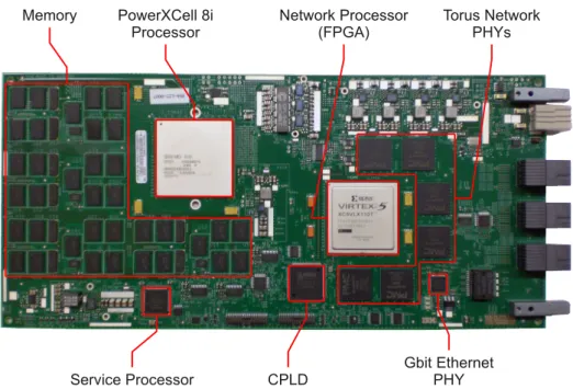
Figure 2.3: Node-card top view with important functional devices highlighted. Each node-card provides one PowerXCell 8i processor and 4 GByte DDR2 memory onboard. The processor is directly connected to the Xilinx Virtex-5 FPGA which acts as an I/O fabric. Six PMC Sierra XAUI PHYs connect to nearest-neighbour nodes. Support for Gigabit Ethernet is provided by the Gigabit Ethernet PHY. The node-card is controlled by the Service Processor and CPLD.
2.2 Node-card
The node-card is the building block of QPACE. It hosts the components necessary for computation of parallel applications. A photograph of the node-card with important functional devices highlighted is shown in Fig. 2.3. Among them are
• 1 IBM PowerXCell 8i
• 4 GByte DDR2-800-SDRAM onboard
• 1 Xilinx Virtex-5 FPGA (network processor)
• 6 PMC Sierra XAUI physical transceivers (PHY) for nearest-neighbour interconnect
• 1 Gigabit Ethernet PHY
• 1 Service Processor and 1 CPLD for management and control
• Ethernet magnetics, flash memory, voltage connector and regulators, board connectors etc.
Each node-card is managed and controlled by an onboard microcontroller, the so-called Service Processor (SP). Node-card-specific information – such as serial number, voltage settings, boot op- tions, and critical error information – are stored on the Vital Product Data memory (VPD) which is accessible by the SP. The images for the Cell BE Slimline Open Firmware (SLOF) [18] and the FPGA bitstream are stored on the onboard flash memory. The firmware boots the node-card via multicast TFTP netboot into a standard Fedora Linux distribution that was extended to support for the QPACE proprietary devices.
The energy efficiency of the node-card was increased by individual voltage tuning. The core voltage of each individual Cell BE was tuned for operation at low voltage setting (which includes a safety margin). Additional reduction of the energy consumption was achieved by optimization of the main memory voltage margins. Voltage tuning improves the power consumption of QPACE by about 10% and therefore increases the performance per Watt ratio. Details about the voltage tuning are provided in Ref. [19].
2.3 Cooling
Roughly 115 Watts have to be dissipated from each node-card. The node-cards are cooled by water, whereas all other system components rely on conventional passive and active cooling by air. Al- though liquid cooling is not a revolutionary concept in the history of supercomputers, its realization in QPACE addresses the typical disadvantages. Liquid cooling solutions tend to be expensive, main- tenance of critical components may become difficult, and electronic devices are seriously damaged when exposed to water. Innovative strategies were introduced to tackle these drawbacks.
The main producers of heat, the node-cards, are packed in housings made of aluminium. The heat is conducted from the components – in particular the Cell BE, FPGA, PHYs, memory chips, and voltage converters – to the surface of the housings. Up to 32 housings are mounted on a flat, water-cooled coldplate made of aluminium. Water-conducting channels inside the coldplate transfer the heat from the node-cards to the liquid circuit. Only a small interfacing area of about 40 cm2 is necessary for heat transfer from each housing to the coldplate. Thermal contact between the housing and the coldplate is improved by a thin film of synthetical oil. The benefits of the two-component cooling design are summarized in the following:
• The temperature difference between the water inlet and the processor cores is lower than 40◦C.
• Water inlet temperature on the order of 40◦C is possible (without violation of the chips’
temperature specifications).
• The cooling design allows for high packaging density.
• The housings and electronic components are never exposed to water.
• The water circuit stays closed on maintenance operations.
• The node-cards are easily maintained. Hot-plugging is supported.
• No expensive mechanical parts are required.
The concept of the cooling solution and a photograph of a fully populated coldplate are shown in Fig. 2.4. Further details on the QPACE cooling mechanism are provided in Refs. [19, 20], and general aspects of liquid cooling in high-performance computing are discussed in Refs. [21, 22].
2.4 Communication networks
2.4.1 Torus network 2.4.1.1 Characteristics
The torus network was designed for high-speed inter-node communication with low latency. For each node the torus network provides the connections to six nearest-neighbour nodes in a 3-dimensional mesh. In contrast to high-speed networks of other supercomputers based on the Cell BE, the QPACE architecture is optimized for direct communication between the Local Stores (LS) of adjacent processors. Characteristics of the torus network are:
2.4 COMMUNICATION NETWORKS 11
Figure 2.4: The figure on the left shows the QPACE cooling concept. Node-cards mounted in aluminium housings are attached to an aluminium coldplate. Heat is conducted from the housings to the coldplate at the interfacing area (indicated by the red stripe). The photograph on the right shows the backplane fully populated with 32 node-cards and two root-cards. Manifolds are mounted on the left side of the rack and connect the coldplate to the cooling circuit. Three power supply units per backplane are attached to the right side of the rack.
• High-speed connection based on 10 Gigabit Ethernet physical layer with a peak throughput of 1 GByte/s per link bi-directional.
• Application-optimized link layer with support for slimline datagrams of fixed size of 128 + 4 + 4 bytes (payload + header + CRC).
• Optimization for direct LS-to-LS and LS-to-main memory (MM) communication: Direct mem- ory access (DMA) from the local LS to the remote LS or MM without additional buffering.
LS-to-LS latency ofO(3)µs.
• Runtime support for partitioning.
2.4.1.2 Communication concept
In the following a simplified overview on the communication concept for the torus network is pro- vided. Detailed reviews of the underlying hardware concepts, their implementation, and the perfor- mance of the network are provided in Refs. [20, 23, 24, 25].
The QPACE torus network is optimized for direct communication between two SPEs on adjacent Cell BEs without the need for additional buffering. The data transfer is driven directly by the SPE’s DMA engine. No copy operations from/to main memory are required. This approach grants the application access to the full memory bandwidth, because network I/O operations are removed from this performance-critical data path.
To allow for low-latency communication between adjacent Cell BEs any communication overhead was removed from the torus data path. The sending device pushes data onto its network proces- sor, which autonomously passes the message along the 10 Gigabit Ethernet link to one of its six neighbours. Data is finally pushed by the network processor logic onto the receiving device on the Cell BE. There is no negotiation between the sender and receiver. Minimal support for flow control is granted by a credit mechanism: the network processor streams data onto the receiving device only if a credit is provided to the network processor. After the copy operation a notification is sent to the receiver.
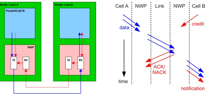
Node−card A Node−card B PowerXCell 8i
NWP
TX RX TX RX
Figure 2.5: The left panel shows the data (blue) and control (red) paths for the torus network.
Each datagram transmitted between adjacent network processors (NWP) is authenticated by a (not) acknowledge packet ACK (NACK). In case of not-acknowledge (NACK) the packet is re-transmitted.
The right panel shows the time flow of the torus communication process.
Any SPE can be source- and endpoint for communication. This feature requires multiple pairs of SPEs on neighbouring nodes to share the same physical link for communication along the 3- dimensional torus. The QPACE torus network supports for eightvirtual channels for each link and direction, which effectively allows for logical separation of up to eight sender and receiver pairs per link and per direction.
The torus network software stack comprises a set of low-level communication primitives designed for the SPE. Details about DMA operations and the hardware structure of the network processor are hidden from the user. The simple but effective torus communication pattern is based on matched send and receive commands, see Ref. [26] for full reference of the torus API. The low-level interface requires the following steps to be executed:
1. Initialization of the receive operation by providing for a given link and virtual channel a credit to the network processor.
2. Data is copied to the network processor by the sender. The largest packet size supported is 2048 bytes.
3. Polling of the notification address, typically in the LS, while waiting for the data to arrive.
After completion of the first two steps the network processor handles the communication au- tonomously. The time between sending the data and receiving the data can be used by the commu- nicating devices for other operations, e.g., for computation or other data load and store operations, including further network transfers. Data, control, and time flow of the torus communication are shown in Fig. 2.5.
2.4.1.3 Partitioning
The torus network supports for a variety of partitions within the 3-dimensional mesh. On a single backplane the logical volume of nodes can be as large (x, y, z) = (1,4,8). In y-direction the number of nodes is increased by vertical connections of adjacent backplanes using cables (intra-rack). In a
2.4 COMMUNICATION NETWORKS 13 similar fashion the x-direction is extended by horizontal connections of adjacent backplanes using cables (inter-rack). Different partitions are created by switching between two serial interfaces of the PMC Sierra PHY. Some of the serial interfaces are connected to additional traces on the backplane that allow for various connections between the nodes. Switching between the primary and redun- dant interface of the PHYs is performed by software during runtime. The following partitions are supported by the QPACE architecture:
• 1, 2, 4, 8 nodes in thez-direction.
• 1, 2, 4, 8, or 16 nodes in the y-direction.
• 1, 2, or 2N nodes in thex-direction (here N is the number of interconnected racks).
2.4.2 Ethernet network
The switched Ethernet network connects the node-cards, root-cards, and superroot-cards to the front-end system. The front-end comprises one master server used for machine control and manage- ment, one login server which serves as central user access point, and several I/O servers dedicated to the Lustre parallel file system. The Ethernet network is divided into I/O, machine management, and control sub-networks. It also provides connection to the outside world. A closer look on the arrangement of these sub-networks will be taken in Sect. 2.5.2.
Eack QPACE rack provides 24 1-Gigabit Ethernet uplinks for connection of the node-cards to the front-end system. The external bandwidth is on the order of 2 GByte/s per rack, which is also supported by the local disk storage systems. The throughput is sufficient to sustain the compute performance for non-I/O intense applications such as Lattice QCD.
2.4.3 Global signals network
The global signals (GS) network is a simple but effective two-wire tree network with support for partitioning. Information exchange is based on the state of the global signals network. There is no (native) support for packet-based communication. The capability of the GS network is limited to three active states and one idle state. The active states are used to evaluate global conditions and to distribute an exception signal in the case of a compute-critical error. Global conditions are used, e.g., to synchronize the nodes by creation of a barrier. Parallel jobs can be terminated by the global kill signal. Communication along the GS network proceeds in the following steps:
1. Node-cards assigned to the partition propagate the signals NOP, TRUE, FALSE, or KILL to the so-called root logic.
2. The root logic is coded into programmable devices hosted by the root-cards and superroot- cards. These cards serve as end-points for local (and global) OR and AND operations within the GS network hierarchy. The reduced information is propagated up the hierarchy until the end-point is reached.
3. The result of the global reduction operation is propagated down along the hierarchy to the node-cards.
The global signals network was designed to support for all partitioning options granted by the torus network. See Ref. [27] for more information on the global signals tree network.
2.5 System setup
2.5.1 Front-end system
The front-end system (FES) is the interface between the user and the back-end, i.e., the QPACE racks. The FES consists of dedicated servers and interconnects. The FES is integrated into a single rack and serves the following purposes:
• Provide the physical connections between the QPACE racks, front-end servers, and the outside world by the Gigabit Ethernet switch layer.
• Grant access to the Lustre parallel file-system.
• Support for job scheduling by the batch queueing system.
• Support for maintenance operations and administration.
• Control and monitoring of the system by automated software services.
The master server acts as the portal to the system. The master server runs the batch queueing system, the front-end service daemon, and system monitoring services. The login server allows the users to login to the system from the outside world, to schedule and maintain jobs, and access data stored on the Lustre parallel file-system. Support for the Lustre file-system is provided by dedicated metadata and object storage servers. More information about the FES aiming at both administrators and users is provided at the QPACE homepage at DESY, Ref. [28].
2.5.2 Ethernet networks
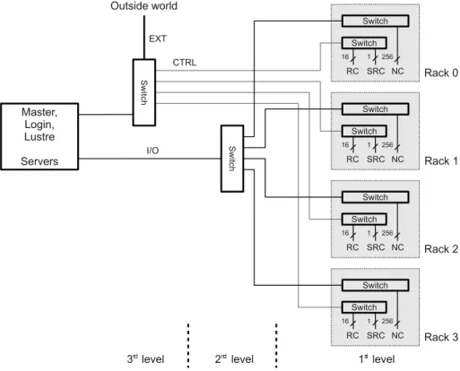
The Ethernet network is organized as a layered switched network system. It is divided into multiple virtual sub-networks. Multiple switches per layer are stacked, i.e., several physical switches are combined and act as one logical switch with the port capacity of the sum of the single switches. The advantages of the stacked setup are the simplified administration by reduced IP numbers, reduced cabling, and the high inter-switch throughput provided by the dedicated stacking bus.
The layered Ethernet network and the virtual sub-networks for the QPACE installation at the University of Wuppertal are shown in Fig. 2.6. The three layers consist of:
1st layer Each QPACE rack consists of stacked switches that connect to the node-cards. Per rack another dedicated switch connects to the root-cards and the superroot-card.
2nd layer One stacked switch connects the front-end servers, I/O servers, and the racks.
3rd layer Additional switches connect the FES to the outside world and to the administrative networks.
Four Virtual Local Area Networks (VLAN) are configured on top of the switched network. VLANs allow for multiple private networks sharing the same hardware resources. The Ethernet network is subdivided into
• I/O network: Connection between front-end servers and node-cards.
• Control network: Connection between master server, root-cards, and superroot-cards.
• Management network: Connection between the management Ethernet devices in the front-end.
• External network: Connection to the outside world.
2.6 OTHER SYSTEM COMPONENTS 15
Figure 2.6: Simplified overview of the Ethernet switched network. The external network (EXT) connects the front-end system to the outside world. The I/O network connects the front-end servers and node-cards (NC). The control network (CTRL) grants the master server access to the root-cards (RC) and superroot-cards (SRC).
2.6 Other system components
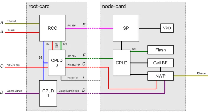
2.6.1 Root-card
The root-card serves multiple purposes. One of them is the support for administration of the node-cards. Up to 16 node-cards are controlled by the root-card. Two root-cards handle the thirty- two node-cards attached to the backplane. In total 16 root-cards control a complete QPACE rack comprising 256 node-cards. The root-cards are attached to the Ethernet control network described in Sect. 2.5.2 and are controlled by the master server.
The root-card also provides the logic for handling of the global signals network and distributes a global clock signal. This clock signal, which is generated by an oscillator on the master root-card and gets distributed amongst all other root-cards within a tree network, serves as the reference clock for the torus network logic on the network processor on the node-card. The purpose of the global clock is to maximize the clock alignment at the torus transmit and receive logic. The torus reference clock can be switched between the global clock signal and a local clock signal that is generated individually on each node-card.
The root-card provides connections to the node-cards, the Ethernet control network, and the global signals network. Relevant data paths are shown in Fig. 2.7. Each root-card hosts one micro- controller (RCC) and two complex programmable logic devices (CPLD). CPLD 0 acts as switch for reset lines, UART, and SPI. CPLD 1 hosts the logic that handles the global signals (root logic). In the following each connection shown in Fig. 2.7 is briefly described:
A 100 Megabit Ethernet connection to the Ethernet control network.
Figure 2.7: Root-card data paths and connections to the node-cards. Only a single node-card is shown.
B One connection to the RCC via RS-232 (mode 8N1), serving as failover data path. The UART of the RCC is accessible by the debug connector.
C Sixteen connections RS-232 (mode 8N1) from CPLD 0 to the node-card network processors (NWP). This data path allows for monitoring and control of the Cell BE firmware (SLOF) during the boot process and grants access to the Linux console. Each NWP is accessible by either the RCC or an external connection by the debug connector. Only one NWP can be accessed by the RCC at a time.
D Connection to the global signals network. CPLD 1 handles the uplinks and downlinks within the tree network. The global signals logic performs the reduction and distribution of the signals along the partition.
E The RS-485 multi-drop bus provides connections between the RCC and 16 Service Proces- sors (SP). The RCC acts as the master, while the SPs are slaves on the bus. Communication is limited to one RCC-SP connection at a time. The communication protocol is proprietary.
F The SPI interface of the RCC is multiplexed by CPLD 0 and allows for access to the flash memory of the node-cards. The flash memory stores the SLOF image and the FPGA bitstream. Only one flash memory device is accessible at a time.
G Control of CPLD 0 and 1 by the RCC via I2C.
I Sixteen reset lines to the node-cards. Each node-card can be hard-reset individually.
The RCC is operated by an embedded Linux operating system with support for the common Ethernet software stack [29]. The Linux image is loaded on power-on of the RCC via TFTP netboot. Custom- designed software libraries provide remote access to the root-card from the master server. The
2.6 OTHER SYSTEM COMPONENTS 17
Figure 2.8: Superroot-card data paths. Only a single PSU is shown.
feenlib software library1 provides low-level functions for control of the RCC and CPLDs. The witchlib software library was built on top of the feenlib library. It provides a series of high-level functions that, e.g., allow for control of the node-cards. The libraries are accessed by several test and administration tools, see Sect. 5.3 for an example. The API of the witchlib library is provided in Appendix A.3.
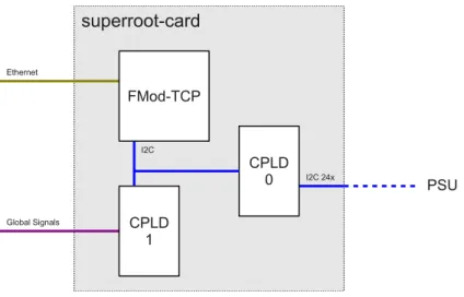
2.6.2 Superroot-card
Each QPACE rack hosts one superroot-card. The superroot-card monitors and controls the power supply units (PSU). It also handles the global signals at rack top level. The superroot-card connects to the Ethernet control network by the FMod-TCP device [30]. The FMod-TCP essentially consists of a microcontroller unit that allows for remote control of its interfaces via the embedded TCP/IP stack. The controller comes with a variety of standard interfaces, e.g., Ethernet and I2C. The I2C bus establishes a connection between the FMod-TCP and two CPLDs mounted on the superroot- card. CPLD 0 provides another 24 I2C connections accessible by the FMod-TCP. Each of them is dedicated to one of 24 PSUs (with corresponding I2C expansion cards) attached to the rack, effectively providing support for remote power monitoring and PSU management. CPLD 1 hosts the global signals root logic and connects to the global signals network. Multiple superroot-cards are interconnected such that the global signals tree spans all racks. See Ref. [27] for more information on the global signals tree network. The software libraries for the superroot-card were custom-designed and allow for control of the superroot-card from the master server.
1feenlibwas written by S. Solbrig.
Chapter 3
The IBM Cell Broadband Engine
3.1 The Cell Broadband Engine and the supercomputer league
The Cell Broadband Engine (Cell BE) is a powerful microprocessor developed by Sony, Toshiba, and IBM – the STI alliance – in the years 2001 to 2005. The initial target platform of the Cell BE was the consumer electronics market, especially the PlayStation 3 gaming platform. Whilst the initial version of the processor had limited floating-point performance for calculations in double precision, the revised variant called PowerXCell 8i removed this barrier in 2008. The high floating- point performance of the PowerXCell 8i rendered this processor an interesting option for scientific applications [31]. Besides the outstanding performance in number crunching its superior energy efficiency, typically measured in Flops per Watt, kicked supercomputers based on the PowerXCell 8i on top of the Green 500 list from June 2008 to June 2010 [14].
The most prominent supercomputer that comprised Cell BE technology was the RoadRunner cluster at the Los Alamos National Laboratory [32]. The hybrid architecture hosted more than 6000 AMD Opteron and 12000 IBM PowerXCell 8i processors connected by Infiniband technology. With more than 100000 processor cores distributed amongst 296 racks the cluster hungered for more than 2 MW of power. In the year 2008 RoadRunner was not only the first supercomputer to break the PFlops barrier in sustained performance, it was also amongst the top ten supercomputers in terms of energy efficiency achieving 458 MFlops per Watt [1, 14]. Roadrunner was decommisioned in early 2013.
In the years 2009 and 2010 the success of the Cell BE continued with a new world record.
The QPACE supercomputer at the J¨ulich Supercomputer Centre and the University of Wuppertal achieved 773 MFlops per Watt in the Linpack benchmark. The QPACE architecture was almost 60%
more energy efficient than the Chinese Nebulae hybrid CPU/GPU supercomputer at the National Supercomputing Centre in Shenzhen (NSCS). Nebulae was the second-best system on the Green 500 list in June 2010 and achieved 492 MFlops per Watt [14].
3.2 PowerXCell 8i overview
Due to the complexity of the Cell BE architecture this section focuses only on its most striking characteristics. Further details on introductory level are presented, e.g., in Ref. [33]. For full architecture and programming details see Refs. [34, 35].
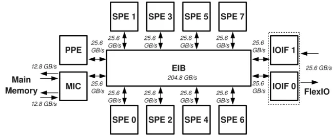
A schematic diagram for the processor is shown in Fig. 3.1. The PowerXCell 8i is a heterogeneous microprocessor that contains nine physical processing units, namely one 64-bit PowerPC Processor Element (PPE) and eight Synergistic Processor Elements (SPE). Each SPE has 256 kByte of local memory (the Local Store, LS) available, accessible by a dedicated direct memory access (DMA) engine. The register file comprises 128 general-purpose registers, each of them 128 bits wide. The
19
Figure 3.1: Schematic diagram for the IBM PowerXCell 8i. The processor consists of one Power Processor Element (PPE) based on a PowerPC core, eight Synergistic Processor Elements (SPEs), coherent and non-coherent I/O interface (IOIF), and a memory controller (MIC). All units are connected by the element interconnect bus (EIB). The bandwidth values are shown for the 3.2 GHz system clock.
SPE is a single-threaded, dual-issue in-order processor with support for single-instruction multiple- data (SIMD) operations. SIMD instructions perform up to four single precision (SP) or two double precision (DP) floating-point operations simultaneously. The Cell BE’s floating-point arithmetic is compliant to IEEE standard 754.1 At a system clock frequency of 3.2 GHz the outstanding aggregate SP (DP) peak performance of all eight SPEs is 204.8 (102.4) GFlops.2
The PowerXCell 8i’s on-chip dual-channel DDR2-SDRAM memory interface controller (MIC) delivers a peak memory bandwidth of 25.6 GByte/s. The Rambus configurable I/O interface (IOIF) supports a coherent and a non-coherent protocol with a peak bi-directional bandwidth of 25.6 GByte/s. Internally, all twelve units are connected to the coherent element interconnect bus (EIB) that handles multiple DMA requests simultaneously.
It is worth to mention that the PowerXCell 8i supports for error-correcting code (ECC) of the Local Stores (LS) and also main memory (MM). Data integrity seriously suffers from spontaneous bit flips caused by electromagnetic interference and background radiation. ECC-capable memory allows to mitigate this problem (at the cost of extra storage) and typically supports for either detection and correction of a single bit error, or detection of a double bit error, per 64-bit word.
3.3 Lattice QCD on the Cell BE
The performance of any application relies on the efficient implementation of relevant compute kernels on the underlying hardware structure. Performance models serve as guides to the best implementa- tion of the algorithms and give hints on the optimal data layout and code-optimization strategies. A hardware abstraction model along the lines of Ref. [40] was developed in the initial phase of QPACE
1A biased comment by Intel with emphasis on the importance of floating-point arithmetics standardization is provided in Ref. [36]. It is illuminating to continue reading with Ref. [37].
2For comparison, the Intel Xeon E7-8870 Westmere-EX server CPU introduced in the year 2011 achieves an ag- gregate peak performance of 96 (48) GFlops in SP (DP) executing up to 4 (2) Flop per core per cycle clocking all 10 cores at nominal frequency of 2.4 GHz [38]. The nVidia Tesla M2090 GPU, also introduced in the year 2011, achieves 1331 (665) GFlops peak in SP (DP) running 512 compute cores in parallel at a clock frequency of 1.3 GHz [39].
3.3 LATTICE QCD ON THE CELL BE 21
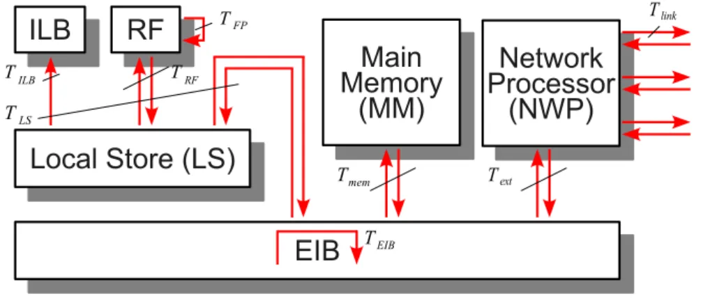
Figure 3.2: Data-flow paths and execution times Ti of micro-tasks considered in the performance model. For simplicity only a single SPE is shown.
that allowed to estimate the performance of the most relevant Lattice QCD kernel for Wilson-type fermions. The model was published in Refs. [41, 42] and is discussed in the following.
3.3.1 Performance model
The performance model is based on the abstraction of the Cell BE hardware architecture. The model relies on the abstraction of the hardware into two classes of devices:
(i) Storage devices, storing data and/or instructions (e.g., registers, LS, and MM).
(ii) Processing devices, acting on data or transferring data/instructions from one device to another (e.g., FP units and data buses).
The operations performed by the Lattice QCD kernel can be decomposed into “micro-tasks” which are mapped to the hardware devices. It is assumed that all micro-tasksiperformed by the processing devices are running concurrently at maximal throughputβi, and all latenciesλiare hidden by suitable scheduling. Any data dependencies are neglected. The execution timeTi of each taskiis estimated by the linear ansatz
Ti'Ii/βi+O(λi), (3.1)
whereIi is the amount of data to be processed. The hardware devices, data-flow paths, and associ- ated micro-task execution timesTi considered in the performance model for the Lattice QCD kernel are shown in Fig. 3.2. Among them are
• Execution of floating-point operations (TFP).
• Load of instructions into the instruction look-aside buffer (TILB).
• Load/store operations between the register file and LS (TRF).
• Off-chip memory access (Tmem).
• Internal communications between SPEs (Tint).
• External communications between adjacent Cell BEs (Text).
• Transfers via the EIB (TEIB).
All devices are running in parallel in this model (at maximal throughput) and the kernel is mapped to eight SPEs.3 The estimate for the total execution time Texe of the kernel is
Texe'max
i Ti , (3.2)
thus the execution time is dominated by the most time-consuming micro-task. The identification of this task allows to determine the floating-point efficiency εFP. Let Tpeak be the minimal compute time of the kernel, achieved by an ideal implementation that saturates the floating-point performance of the Cell BE, then the floating-point efficiency is defined as εFP =Tpeak/Texe.
3.3.2 Lattice QCD kernel
For applications in Lattice QCD with Wilson-type fermions the 4-dimensional hopping term Dh of the Wilson-Dirac operator is the most performance-relevant kernel. The Wilson-Dirac operator is discussed in more detail in Sect. 6.6.1. All compute-intensive tasks, e.g., solving a system of linear equations, involve its repeated application to a quark field ψ,
ψx0 =Dhψx =
4
X
µ=1
n
Ux,µ(1 +γµ)ψx+ˆµ+Ux−ˆ† µ,µ(1−γµ)ψx−ˆµ
o
. (3.3)
Here x = (x1, x2, x3, x4) is a 4-tuple of coordinates labelling the lattice sites in a discretized 4- dimensional Euclidian space-time volume. The quark fields ψx0 and ψx are spin-colour vectors as- signed to each lattice site x. The vectors consist of twelve complex numbers each. A colour matrix Ux,µ ∈SU(3), consisting of nine complex numbers, is assigned to each link from sitex in one out of four space-time directions ˆµ. Theγµare 4×4 Dirac matrices.
The most efficient way to floating-point performance is to exploit the SIMD instruction set of the SPE. The dual-issue SPE supports for concurrent execution of up to two fused multiply-add operations that compute a×b+cwith real operands.4 Thus up to four floating-point operations in double precision can be executed per clock cycle. On a single lattice site the computation of Eq. (3.3) amounts to 1320 floating-point operations (neglecting sign flips and complex conjugation). Let the computation perfectly match the instruction set architecture (ISA), i.e., the peak floating-point throughput is saturated, then the minimal compute time is Tpeak = 330 cycles per site. However, the multiply and add arithmetics arising in the hopping term are not adequately balanced, and the implementation of the operator requires at least 840 fused multiply-add operations. The execution time isTFP ≥420 cycles per site due to the imbalance. Therefore any implementation of Eq. (3.3) cannot exceed 78% of the peak performance of the Cell BE.
3.3.3 Data layout analysis
State-of-the-art simulations of Lattice QCD carry out calculations on global volumes that consist of 643×64 or even more lattice sites. Thus massive amounts of data need to be distributed on a large number of nodes to be efficiently dealt with. The choice for the data layout on the nodes is crucial for the performance of the Lattice QCD kernel, and the optimal choice for the layout can be found with the performance model introduced above.
Let the lattice sites be partitioned regularly among the nodes, and the local lattice volume assigned to each Cell BE be denoted by VCell. According to the definition of the hopping term Eq. (3.3), data has to be communicated along four dimensions. However, only the information associated with the surface of the local lattice volume has to be communicated between neighbouring
3The PPE is rather weak in floating-point performance and is not taken into account.
4There is no native support for complex numbers on the Cell BE.
3.3 LATTICE QCD ON THE CELL BE 23 nodes. The time spent on possible remote communications and on load/store operations of the 9×12 (for theψ-fields) and 8×9 (for the U-fields) operands of the hopping term strongly depends on the data layout. For the following discussion of the data layout it is assumed that all floating-point numbers are represented in double precision (8 bytes).
The design of the QPACE torus network allows each Cell BE to exchange data with six nearest- neighbours in the mesh. With the constraint of a 3-dimensional physical network that connects neighbouring nodes, one space-time direction must be distributed locally within each Cell BE. For convenience the 4-direction is chosen here. Each Cell BE is assigned the fraction
VCell=L1×L2×L3×L4 (3.4)
of the global lattice volume. The number of sites locally distributed amongst the SPEs is
VSPE= (L1/s1)×(L2/s2)×(L3/s3)×(L4/s4) =VCell/8, (3.5) with the SPEs logically arranged ass1×s2×s3×s4 = 8. There are strong limitations to the amount of application data stored on the SPEs. Besides the application data, the LS must also hold the program code, intermediate data, and the run-time environment. For the implementation of a solver one needs access to 8 Dirac spinors and 3×4 colour matrices per lattice site.
Data stored in on-chip memory
One possibility for the data layout is to keep all data in the LS only. Due to the strong constraints on storage the local lattice volume is then restricted toVSPE =O(70) lattice sites assigned to each SPE. Since all data associated with the 4-dimension must be kept within the Cell BE, a reasonable choice is L4 = 64 and a logical arrangement of the SPEs by 13 ×8. This data layout yields an asymmetric local lattice with VCell= 23×64 andVSPE = 23×8.
Data stored in off-chip memory
Another possibility is to store the data in main memory. The implementation of a multiple buffering scheme allows for concurrent computation and data load/store from/to memory main and SPEs.
The hopping term Eq. (3.3) is computed on a 3-dimensional slice of the local lattice that moves along the 4-direction. Each SPE stores all sites along the 4-direction, and the SPEs are logically arranged as a 23×1 grid. If theU- andψ-fields associated with all sites of three such slices are kept in the LS at the same time, then all relevant operands are available in the LS. This optimization requirement constrains the local lattice toVCell/L4≈800 sites.
Given the ansatz for the data layout, the execution time of the micro-tasks arising in the computation of the hopping term Eq. (3.3) were estimated by Eq. (3.1). The throughput for external communica- tion was assumed to sustain5 βext= 6 GByte/s with a link bandwidth ofβlink= 1 GByte/s per link and direction. Other relevant information about the Cell BE was taken from public sources. The estimated execution times are shown in Table 3.1 for reasonable sizes of the local lattice. If all data is stored on-chip the sustained performance is limited by remote communications, and the floating- point efficiency is about 27%. In contrast, if all data is stored off-chip the memory wall limits the maximum performance and one can expect to achieve up to 34% efficiency for the implementation of the kernel. Although the performance estimate for both data layouts does not differ significantly, data storage in main memory is the favoured choice. The constraints on remote communications are relaxed, but code optimizations for efficient main memory access become crucial.
5The design goal for the external throughput was 6 GByte/s. However, in the recent implementation of the QPACE network processor the external throughput is about 3 GByte/s.