Interaction of Graphene and Templated Cluster Arrays
with CO, H 2 , and O 2
I n a u g u r a l - D i s s e r t a t i o n zur
Erlangung des Doktorgrades
der Mathematisch-Naturwissenschaftlichen Fakultät der Universität zu Köln
vorgelegt von
Dipl.-Phys. Timm Gerber
aus Offenbach am Main
Vorsitzender
der Prüfungskommission: Prof. Dr. Joachim Krug Tag der mündlichen Prüfung: 31. Mai 2013
Abstract
Interaction of graphene and templated cluster arrays with CO, H2 and O2 was stud- ied by means of scanning tunneling microscopy (STM) and X-ray photoemission spectroscopy (XPS). The experimental data was complemented by ab initio density functional theory (DFT) calculations. As a prerequisite for studies of gas interac- tion, the binding mechanism of the clusters to graphene, as well as the growth and structure of Pt clusters, was investigated in detail.
The formation of cluster lattices on graphene on Ir(111) has been explained by graphene rehybridization. This DFT picture was tested by comparing calculated core level spectra to XPS measurements. For pristine graphene, DFT and XPS agree on a 140 meV modulation of the C 1s core level shifts (CLS), which correlates with the height modulation of the graphene layer above the Ir surface. With Pt clusters adsorbed, measured Pt 4f CLS of the adsorbed clusters also support the calculations. The modulation of the C 1s spectrum is strengthened with clusters adsorbed, and C atoms both under and in the vicinity of the Pt clusters are exper- imentally distinguished as a broad shoulder of positive C 1s CLS. The calculations suggest that the sp2 to sp3 rehybridization of graphene displaces the involved C atoms closer to the Ir(111) surface, implying chemical bond formation. The signa- ture of these bonds in the Ir 4f spectrum was identified.
The growth of Pt clusters, their structure, and their interaction with the graphene layer was studied as a function of Pt coverage. STM measurements revealed that once Pt clusters are two-layered, their further growth is restricted to two dimensions.
The threshold for sintering was found to be at 0.75 ML Pt, so that the upper size limit for Pt clusters arranged in a lattice is 65 atoms. The cluster-graphene interaction, as well as the graphene-Ir surface interaction was investigated with spectra of the C 1s and the Ir 4f regions, respectively. It was found that the related components, namely the C 1s shoulder and the Ir interface component, agree regarding their relative intensities. Combining these results, schematic representations of the clusters and
iii
their binding geometry with the graphene layer was derived.
Pt cluster arrays were tested for their stability with respect to CO gas exposure.
Cluster stability and adsorption-induced processes were analyzed as a function of cluster size. Small clusters containing fewer than 10 atoms are unstable upon CO adsorption. They sinter through Smoluchowski ripening – cluster diffusion and coalescence – rather than the frequently reported Ostwald ripening mediated by metal-adsorbate complexes. Larger clusters remain immobile upon CO adsorption, but become more three-dimensional. An implication of the CO-induced cluster mobility is the sensitivity of Pt cluster array growth to the CO background pressure.
In order to generalize the results, the study was extended to the adsorption of other gases (H2, O2) on Pt clusters, as well as to the adsorption of CO on other metal clusters (Ir, Au).
The temperature, time and flake-size-dependent intercalation phases of oxygen un- derneath graphene on Ir(111) formed upon exposure to molecular oxygen were stud- ied. Through the applied pressure of molecular oxygen, the atomic oxygen created on the bare Ir terraces is driven underneath the graphene flakes. The importance of substrate steps and of the unbinding of graphene flake edges from the substrate for the intercalation is identified. Using CO titration to selectively remove oxygen from the bare Ir terraces, the energetics of intercalation were uncovered. Cluster deco- ration techniques were used as an efficient tool to visualize intercalation processes in real space. To give an outlook, the study was extended to the intercalation of hydrogen.
Intercalation of graphene often leads doping of graphene. Comparing XPS and angular resolved photoemission spectroscopy (ARPES) data for various systems, it was found that the Dirac point and the C 1s core level shift in the same direction.
These shifts can be described in terms of a rigid band model and the C 1s core level shift may be used to estimate the level of doping. It was found that graphene/Ir(111) is p-doped by H and O intercalation, whereas it is n-doped after Eu intercalation.
The graphene layer is also doped by Pt and Ir clusters on top of it. The smallest clusters n-dope the graphene by charge spill-out. The largest Pt coverage results in a slight p-doping of the graphene layer. When Pt clusters coalesce upon CO exposure, the level of doping is reduced.
Contents
Abstract iii
Contents vii
1 Introduction 1
2 Background 5
2.1 Graphene/Ir(111) . . . 5
2.2 Clusters on Graphene/Ir(111) . . . 9
2.3 Electronic Structure of Graphene . . . 16
2.4 Intercalation of Graphene . . . 20
3 Experimental 25 3.1 The Ultra High Vacuum System TuMA III . . . 25
3.2 Principle of X-ray Photoemission Spectroscopy . . . 27
3.3 The Beamline I311 at Max-lab . . . 30
3.4 Experimental Procedures and Calculations . . . 33
4 How Pt Clusters Bind to the Graphene Moiré on Ir(111) 37 4.1 A Test Case: Core Level Spectrum of Pristine Gr/Ir(111) . . . 38
4.2 C 1s Core Level Shifts of Gr/Ir(111) with Pt Clusters . . . 41
4.3 Ir 4f Signature of Graphene Interaction with the Ir Surface . . . 45
4.4 Pt 4f Core Level Shifts of Pt Clusters Adsorbed on Gr/Ir(111) . . . . 48
4.5 Conclusions . . . 49
5 Growth and Structure of Pt Clusters 51 5.1 Growth Mode of Pt Clusters on Gr/Ir(111) . . . 51
5.2 Cluster-Graphene Interaction Monitored in Ir 4f and C1 s . . . 55
5.3 Correction for Damping and Schematic Representation . . . 60
v
5.4 Pt 4f Spectra . . . 64
5.5 Conclusions . . . 65
6 CO-Induced Smoluchowski Ripening of Pt Cluster Arrays 67 6.1 STM View of Pt Cluster Arrays Exposed to CO . . . 68
6.1.1 Relevance of Tip-Cluster Interactions . . . 73
6.1.2 Quantitative Analysis of Cluster Mobility . . . 77
6.2 Adsorption Site Determination by XPS . . . 78
6.3 Weakening of Cluster-Graphene-Interaction Monitored in C 1s and Ir 4f 81 6.4 DFT Results and the Diffusion Mechanism . . . 84
6.5 Growth of Pt Clusters in the Presence of CO . . . 91
6.6 Generalization to Other Gases and Other Metal Clusters . . . 92
6.6.1 Pt Clusters Exposed to H2 and O2 . . . 92
6.6.2 Ir and Au Clusters Exposed to CO . . . 96
6.6.3 Stability of Clusters at Atmospheric Pressure . . . 100
6.7 Conclusions . . . 101
7 Oxygen Intercalation under Graphene on Ir(111) 103 7.1 Kinetics of Intercalation and XPS Fingerprints . . . 105
7.2 STM View of Intercalation and the Role of Graphene Edges . . . 115
7.3 Energetics of Intercalation . . . 128
7.4 Outlook: Hydrogen Intercalation . . . 132
7.5 Conclusions . . . 136
8 Relation Between Doping of Graphene and the C 1s CLS 139 8.1 Origin of the C 1s Core Level Shift and Doping by Intercalation . . . 141
8.2 Doping by Clusters . . . 147
8.2.1 C 1s CLS Upon CO Exposure . . . 150
8.3 Conclusions . . . 152
9 Summary and Outlook 153 9.1 Summary . . . 153
9.2 Outlook . . . 156
Bibliography 159
Contents vii
Appendix 179
Pt 4f Spectra after Gas Exposure . . . 179
Thermal Desorption Spectroscopy of CO from Pt Clusters . . . 180
Absence of CO Oxidation on Au Clusters . . . 181
Growth of Rh Clusters . . . 182
Publications 185
Symbols and Abbreviations 187
Acknowledgements - Danksagung 189
Deutsche Kurzzusammenfassung 191
Erklärung 193
Lebenslauf 195
1 Introduction
Graphene is a single atomic layer of graphite and thereby represents a two dimen- sional allotrope of carbon. We witness a continuously growing research interest in graphene [1, 2] which is both due to its rich physics and to a variety of possible applications.
A few examples for the former are the ambipolar electric field effect [3], charge carriers which mimic relativistic particles [4], and the unusual half-integer quantum Hall effect [5].
The envisioned applications for graphene-based devices are numerous including high- frequency transistors [6], efficient gas sensors [7], and transparent electrodes for displays [8] or solar cells [9].
One way to fabricate graphene sheets is epitaxial growth on metal surfaces by decom- position of hydrocarbons [10,11]. In this way, graphene layers of exceptional quality can be synthesized on the Ir(111) surface [12,13]. The success of this method stim- ulated attempts to transfer these layers from the substrate onto the desired device [14]. Furthermore, there is a unique characteristic of the graphene on Ir(111) sys- tem, which will be exploited in this thesis: Graphene/Ir(111) is a versatile template for the growth of cluster lattices of unmatched quality [15].
Clusters represent an interesting state of matter. Their structure as well as their elec- tronic, chemical and magnetic properties change with size, and often differ from that of the solid [16,17]. Prominent examples are ferromagnetic clusters of Rh (which is paramagnetic as bulk material) [18], and the unusual reactivity of nanometer-sized Au particles [19].
Moreover, most heterogeneous, industrial catalysts are made of metal particles, a few nanometer in size, dispersed on a porous support [20]. In these systems, the size distribution of the particles is rather broad and their morphology as well as the surface or interface structure is often not known. These variables may not concern an industrial chemist who desires a more efficient catalyst, but who is not disinclined
1
to improve it by trial and error. However, it is the surface scientist’s aspiration to unfold all effects that are involved. Therefore, studies are often performed on supportedmodel catalysts [21]. This term refers to metal clusters prepared on clean surfaces under ultra high vacuum (UHV) conditions which can be examined by surface science techniques. Following this approach, impressive results have been achieved [22]. To name one example, the catalytic activity for the oxidation of carbon monoxide depends on the exact number of atoms constituting Pt clusters supported on MgO [23].
The reactivity of supported clusters is often influenced by their support. For Au clusters supported by oxide surfaces, it was shown that this influence can be at least two-fold: Firstly, by changing the cluster’s electronic structure through charge transfer from the substrate [24], and secondly, by the presence of reactive sites at the cluster oxide interface [25, 26]. Therefore, substrates that do not alter the cluster’s properties are desired, and that are inert with respect to molecules involved in the reaction under consideration. These requirements are fulfilled by graphite and thus, clusters on this support have been extensively studied [21].
As a consequence of the exploding interest in graphene, studies of graphene sup- ported clusters appeared. Some examples are the growth of clusters on solution- based graphene nanosheets [27–29], on few-layer [30] or single layer [31] graphene films cleaved from graphite crystals, as well as on graphene grown on Si-terminated SiC surfaces [32–34]. In some cases, these graphene-supported clusters show inter- esting properties as enhanced electrocatalytic activity for methanol oxidation [27], or enhanced CO tolerance in the hydrogen oxidation reaction in polymer electrolyte fuel cells [28], compared to clusters supported on graphite. The common feature of all mentioned examples is that – as on graphite surfaces – the clusters are randomly dispersed.
For this reason, graphene supported on lattice-mismatched metal substrates is an even more interesting support for clusters. Moiré patterns, which arise from the lattice mismatch between graphene and the metal surface, act as a template for self- assembly of metal clusters. The templating effect of the moiré allows the creation of cluster lattices of equally sized and spaced clusters each residing in an identical envi- ronment. Examples include Pt and other metal clusters on the graphene/Ru(0001) moiré [35–42], Ni clusters on the graphene/Rh(111) moiré [43], and a variety of metallic and bimetallic clusters on graphene/Ir(111) [15, 44–46]. Nevertheless,
3 the perfection of the cluster lattice strongly depends on the metal supporting the graphene film [11]. Of the above mentioned, graphene/Ir(111) induces cluster ar- rays whose exceptional order and narrow size distribution makes them particularly attractive laboratories for fundamental studies of nanocatalysis.
A prerequisite to such studies is the investigation of the stability of the cluster/support system at elevated temperatures and in the presence of reactants, i.e. under reaction conditions. Sintering, a decrease in particle number and corresponding increase of particle size, is a process that deactivates catalysts [47–49].
Case studies of various cluster support systems have shed light on sintering mech- anisms at the atomic level. An important one [50–60] is that under reaction con- ditions, clusters are disrupted and form mobile metal-reactant species which cause mass transport and associated ripening. For example, disruption into single adatoms and formation of mobile surface carbonyls [such as Ir(CO)2] have been observed for clusters of Pt [50, 51], Ir [52–54] and Rh [55] grown on TiO2. Decay of epitaxial Cu islands on Cu(111) and Co islands on Au(111) was found to be promoted in the presence of S through formation of mobile Cu3S3 and Co3S4 complexes [56–58].
The lower sublimation energy of Pd-H compared to Pd was proposed to explain the Ostwald ripening of Pd clusters deposited on SiO2 in a hydrogen atmosphere [59].
Lastly, mobile PtxOy species were identified as the source of Oswald ripening of Pt-particles on Al2O3 [60]. But for clusters supported by graphene, no such studies are available yet.
In the case of graphene supported clusters, exposure to gases may not only influence the particles, but have an impact on the graphene itself. A common interaction of gases with graphene is intercalation. This refers to the insertion of an adlayer of molecules or atoms between the graphene sheet and its substrate. Examples are H and O intercalation under graphene/SiC [61–63] and O intercalation under Graphene/Ru(0001) [64–66].
Beyond gaseous intercalants, graphene can also be intercalated by metals [67–73] or by semiconductors [74–77]. The strong interest in intercalation of graphene stems from unique possibilities to decouple [61–63, 67–69, 74–76] or even electrically in- sulate [77] it from the substrate, or to enable its exfoliation [14]. Furthermore, the graphene may be doped by the intercalated layer [72, 78], which increases the number of charge carriers and thus enhances the conductivity of graphene. Finally, even the properties of the intercalated film may be altered due to the presence of
graphene on top of it [73]. In order to control intercalation precisely, a detailed understanding of the process is desired.
In the following, the content of this thesis is outlined. Before these results are presented, the necessary background information is given (Chapter 2), and the ex- perimental methods are described (Chapter 3). The outstanding ability of graphene on Ir(111) to act as a template for cluster lattices originates from a particular binding mechanism of the clusters to the graphene [79,80]. In Chapter 4, the existing theo- retical model of this binding mechanism is experimentally substantiated. Chapter 5 studies the growth mode of Pt clusters, their structure and their interaction with the graphene layer in detail. In Chapter 6, the stability of clusters on graphene/Ir(111) in the presence of gases is investigated, with a focus on the impact of CO onto Pt clusters. The intercalation of graphene by oxygen, and the impact of this process on clusters on the graphene is described in Chapter 7. Finally, Chapter 8describes how the graphene layer is doped by the presence of intercalated oxygen underneath, or by cluster lattices on top of it, and how this doping is manifested in the C 1s core level shift.
2 Background
2.1 Graphene/Ir(111)
Graphene (abbreviated Gr) can be grown in exceptional quality by decomposition of hydrocarbons on the Ir(111) surface [44, 81, 82]. Several growth recipes yielding either graphene flakes [81] or a closed monolayer of graphene are available [13, 83].
Details on these processes are given in Section3.4.
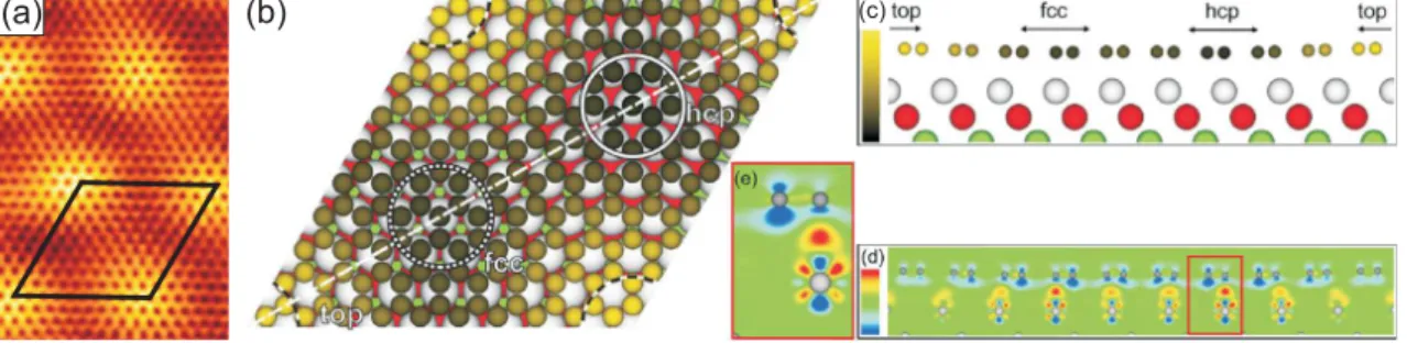
012 032 042
Figure 2.1(a) STM topograph (59 Å×84 Å, U = 1 V, I = 7 nA) of the graphene moiré on Ir(111). Reproduction from [84]. (b) Top view and (c) side view [cut along the dashed line in (b)] of the relaxed structure of graphene/Ir(111) obtained by DFT including vdW interactions. Regions of high-symmetry stacking (fcc, hcp, top) are marked by circles (b) or arrows (c) and (d). The color scale in (b) and (c) ranges from h = 3.20 Å (dark) to h = 3.65 Å (yellow). (d) Charge transfer upon adsorption. The color scale ranges from
∆ρ = -0.0138eÅ−3 (blue) over light green to ∆ρ = +0.013eÅ−3 (red). A negative value indicates loss of electron density. (e) Magnified view of red box in (d). Reproduction from [85].
Figure2.1(a) shows a scanning tunneling microscopy (STM) topograph of Gr/Ir(111).
The small black dots represent the centers of the carbon rings. The long range pat- tern is a moiré superstructure resulting from the mismatch of the graphene and the iridium lattice. The moiré is an incommensurate pattern of (10.32 x 10.32) carbon rings over (9.32 x 9.32) Ir atoms [86].
Figure2.1(b) shows a ball model of the moiré unit cell as calculated by nonlocal van
5
der Waals density functional theory (vdW-DFT) [85]. For the calculations the unit cell was approximated by (10 x 10) unit cells of graphene on (9 x 9) cells of Ir(111).
Three high-symmetry domains exist which are labeled top, hcp, and fcc according to the location of the center of the carbon rings with respect to the Ir(111) surface.
The largest distance of graphene over the Ir surface of 3.62 Å is found in the top regions. These regions correspond to the bright areas in Fig.2.1(a). The hcp and fcc regions have a height of 3.27 Å and 3.29 Å, respectively. The average height of 3.41 Å corresponds very well with the experimental value of 3.38 Å as determined by the x-ray standing waves (XSW) method. This distance is similar to the interlayer distance in graphite of 3.36 Å, and indicates that bonding of graphene to the Ir surface is weak. The height corrugation is due to the fact that bonding is not uniform over the unit cell. While the average height gives the impression of pure vdW interaction, a small charge transfer from graphene towards the substrate takes place in the hcp and fcc regions (Fig.2.1(d) and (e)). In conclusion, the binding with an average binding energy ofEb = -50 meV/C consists of weak chemical bonds in the hcp and fcc areas and chemical repulsion in the top areas.
As we will see, this binding energy inhomogeneity of graphene on Ir(111) influences the process of intercalation (Chapter 7).
The on average weak bonding of the graphene layer to the Ir(111) surface is mani- fested in X-ray photoemission spectroscopy (XPS). Figure 2.2shows C 1s spectra of graphite and graphene on various lattice-mismatched metal substrates by Preobra- jenski and coworkers [87]. The spectrum for graphene/Ir(111) can be reproduced with a single peak which is only slightly broader than the one of graphite. This indi- cates that the bond strength as well as the corrugation are comparable in both sys- tems. We will see in Chapter 4that the width of the C 1s peak for graphene/Ir(111) correlates with the height distribution of the carbon atoms in the graphene unit cell.
Contrarily, the strong chemisorption of graphene on both Rh(111) [88] and Ru(0001) [89] leads to a splitting of the C 1s peak into a weakly bonding and a strongly bonding component.
Before we turn to the description of cluster growth on graphene/Ir(111), we will briefly discuss the morphology of graphene islands on graphene/Ir(111). The model shown in Figure 2.1 was obtained assuming that the graphene layer is of infinite extension. Lacovig et al. [90] investigated how the morphology of small graphene islands differs from that of an infinite layer. Using a combination of DFT and
2.1 Graphene/Ir(111) 7
Figure 2.2 C 1s photoelectron spectra from graphene (here referred to as MG i.e. mono- layer graphite) adsorbed on several lattice-mismatched metal surfaces. The photon en- ergy is 400 eV. The C 1s photoelectron spectrum from highly oriented pyrolytic graphite (HOPG) is shown for comparison. Schematics illustrate the resulting graphene morphol- ogy. Reproduction from [87].
XPS they found that graphene nanoislands adopt a particular domelike shape and that their edges are strongly bound to the substrate (see Figure 2.3). According to these results, one would expect that large graphene islands (consisting of several moiré unit cells) are predominantly bound to the substrate by the carbon atoms at their edges, too. This view is, however, challenged by findings of Li and coworkers [91], who reported that the edges of graphene islands on Ir(111) are terminated by hydrogen. The issue of how the dangling carbon bonds at the edges of graphene islands are saturated is the subject of ongoing research and not settled so far. As the termination of the graphene edges is likely to influence the pathway of intercalation, this will become important in Chapter 7.
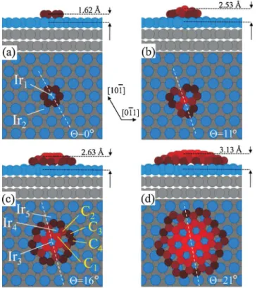
Figure 2.3 Calculated structural models of the carbon clusters formed by n honeycomb rings with (a) n= 1, (b)n = 3, (c)n = 7, and (d)n= 19. Iri and Cj represent different local configurations of Ir and C atoms respectively. The distance of the central C atoms from the Ir substrate as well as the orientation of the cluster with respect to the [10¯1]
direction of Ir(111) is indicated. Reproduction from [90].
2.2 Clusters on Graphene/Ir(111) 9
2.2 Clusters on Graphene/Ir(111)
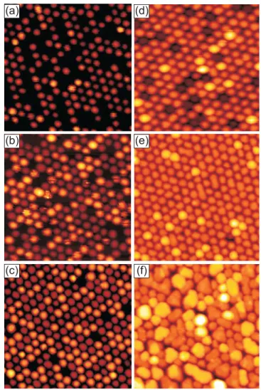
Figure 2.4STM topographs of Ir(111) with graphene flakes after deposition of an amount Θof various metals at 300 K. (a)Θ= 0.20 ML Ir, average cluster sizesav= 17 atoms; (b) Θ= 0.25 ML Pt, sav= 22 atoms; (c)Θ= 0.44 ML W,sav = 38 atoms; (d)Θ= 0.53 ML Re,sav = 60 atoms; (e) Θ= 0.77 ML Fe, s av = 420 atoms; (f) Θ= 0.25 ML Au, sav = 100 atoms. Note thatsav = Θ·Am/nwithAm = 87 atoms the number of Ir atoms in the moiré unit cell and nthe fraction of moiré cells occupied by a cluster (the filling factor).
Image size 700 Å x 700 Å. Reproduction from [15].
Figure 2.4 shows STM topographs after room temperature deposition of the indi- cated metals on Ir(111) partly covered with graphene flakes. Ir, Pt, and W deposition yields cluster lattices close to perfection. At least Ir and Pt cluster grow epitaxially with the (111) cluster planes parallel to the substrate surface. The h1¯10i cluster directions are parallel to the h1¯10i directions of the Ir substrate and the h1¯120i directions of graphene [15]. The epitaxy of Ir clusters on the graphene moiré is supported by a DFT-based model of cluster binding [79, 80].
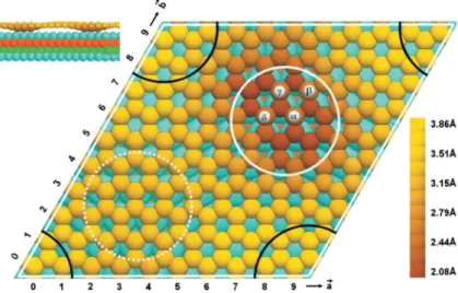
Figure 2.5 Ball model of DFT optimized structure for a four-atom flat Ir cluster on graphene/Ir(111). The unit cell was approximated as (10 x 10) unit cells of graphene on (9 x 9) cells of Ir(111). First, second, and third substrate layer Ir atoms are colored blue, red, and green, respectively. Solid and dotted white circles mark the hcp and fcc regions of the moiré. Top regions, which are delimited by the black arcs, are located in the cell corners. The radii of the Ir adatoms are reduced to reveal the substrate. Local island- induced depression of the graphene layer is shown by the C atom coloring; the color scale denotes heights measured from the Ir surface. Upper left: Side view. Reproduction from [79].
Figure 2.5shows a ball model of an Ir4 cluster adsorbed on graphene on Ir(111). The energetically preferred adsorption site is the hcp region. There the graphene rehy- bridizes from its characteristic sp2 configuration to diamond-like sp3. The graphene layer moves closer to the substrate, with every second carbon atom binding (with its fourth bond normal to the average carbon plane) to Ir surface atoms, while the other half of the carbon atoms bind to the cluster. DFT calculations predict that chemical bonds form between carbon and metal atoms which significantly reduce the local C atom height above the Ir surface from ∼3.4 Å to∼2.1 Å. We note that a similar DFT based scenario has been proposed for patterned adsorption of hydrogen on the graphene/Ir(111) moiré [92, 93].
The favored adsorption site of the Ir cluster (i.e. the hcp region) nicely agrees with the experimental data [86]. Except for this agreement on the adsorption site there has been no experimental proof for this rehybridization model so far. This will be the topic of Chapter 4.
This DFT calculation was performed for an Ir cluster. However, the STM data in Fig.2.4 shows that there is a huge difference in cluster growth for different metals.
2.2 Clusters on Graphene/Ir(111) 11 We conclude that whether the graphene rehybridizes or not strongly depends on the deposited metal. In previous work [15] we considered three factors as heuristic guidelines for the suitability of a material to form a cluster lattice:
(i) A large cohesive strength of the material as an indicator for the ability to form strong chemical bonds.
(ii) A large extension of a localized valence orbital of the deposit material allowing it to efficiently interact with the graphene p-bond and thus to initiate rehybridization to diamond-like carbon underneath the cluster.
(iii) A certain match of the graphene unit cell repeat distance on Ir(111) (2.452 Å [86]) and the nearest-neighbor distance of the deposit material to fit the first layer cluster atoms atop every second C atom.
Table2.1compares these parameters for the studied materials. The guidelines agree with the ability of Ir, Pt, and W to form a cluster lattice and with the inability of Au, Fe, and Ni to do so. The poor quality of the Re cluster lattice is, however, not expected.
Zhou and coworkers [37] suggested that a single parameter suffices to predict cluster lattice formation, namely the (M-C) metal-carbon bond strength. This parameter can be estimated by the M-C bond dissociation energy which is also listed in Table 2.1. Ir, Pt and W show indeed large dissociation energies, whereas the values for Au, Fe, and Ni are much lower. No dissociation energy for Re is indicated as it is well established that rhenium does not form stoichiometric carbides at ambient pressure [94]. Thus, the M-C bond strength is actually a good parameter to predict cluster lattice formation on graphene/Ir(111).
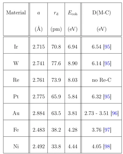
Material a rd Ecoh D(M-C)
(Å) (pm) (eV) (eV)
Ir 2.715 70.8 6.94 6.54 [95]
W 2.741 77.6 8.90 6.14 [95]
Re 2.761 73.9 8.03 no Re-C
Pt 2.775 65.9 5.84 6.32 [95]
Au 2.884 63.5 3.81 2.73 - 3.51 [96]
Fe 2.483 38.2 4.28 3.76 [97]
Ni 2.492 33.8 4.44 4.05 [98]
Table 2.1 Nearest-neighbor distance a, valence d-orbital radius rd, cohesive energyEcoh as well as metal-carbon bond dissociation energy D(M-C) of the tested materials for cluster lattice formation on the graphene moiré on Ir(111). Partly reproduced from [15].
In the following we will compare cluster lattices grown on graphene/Ir(111) to such grown on graphene/Ru(0001). As pointed out in the introduction to this thesis, graphene supported by Ir(111) is the template which fabricates cluster lat- tices of the highest quality in terms of order and size distribution. Its outstanding performance as a template is compared in Figure 2.6(a) to cluster formation on graphene/Ru(0001) [Fig.2.6(b)]. Both samples were prepared by room temperature deposition of ∼0.3 ML Pt onto the graphene pre-covered metal surface. Fig.2.6(a) shows an almost defect free lattice of equally sized clusters. In (b) the moiré pattern of graphene/Ru(0001) is still visible (green pattern) as it is only partially occupied by Pt clusters, which even show a broader size distribution compared to (a).
2.2 Clusters on Graphene/Ir(111) 13
012 032
Figure 2.6 STM topographs after room temperature deposition of (a) Θ= 0.30 ML Pt on graphene/Ir(111) and (b)Θ= 0.36 ML Pt on graphene/Ru(0001). Image size 540 Å x 540 Å. (b) is reproduced from [35].
We note that well arranged Pt cluster arrays on graphene/Ru(0001) can be obtained by Pt deposition at a growth temperature T = 140 - 180 K [36]. Apparently, also for the graphene/Ru(0001) system, there is a preferred nucleation site in the moiré unit cell. However, the variation of adsorption strength over different sites is not as pronounced as for the graphene/Ir(111) system. In the following we will briefly discuss differences in cluster binding on both substrates.
As described above, the clusters grown on graphene/Ir(111) are stabilized in the hcp regions of the moiré unit cell by graphene rehybridization. Underneath the clusters the graphene moves from its vdW bond distance of∼3.4 Å into chemical contact with the substrate. In contrast, the bonding between a pristine graphene layer and the Ru(0001) is strong and cannot be caused by vdW bonds [87,89] (compare Fig.2.2).
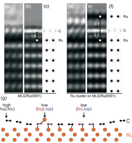
Cluster formation on graphene/Ru(0001) can therefore not be analogous to the case of graphene/Ir(111). Indeed, Sutter at al. [38] showed that Ru clusters adsorb in the low-lying regions of graphene/Ru(0001) where they lift the graphene layer from 1.8 Å to 2.1 Å with respect to the Ru surface (Figure2.7). This binding mechanism is fundamentally different from the one for clusters on graphene/Ir(111) suggested by Feibelman. The latter is apparently a unique property of the graphene on Ir(111) system and most likely the reason for the unmatched quality of the cluster lattices on this template.
012
Figure 2.7 Graphene-Ru separation and its modification by an adsorbed Ru cluster. (a) High-resolution TEM image of monolayer graphene on Ru(0001). (b) Calculated high- resolution TEM image for a graphene-Ru separation of 1.8 Å, giving the best match be- tween experiment and simulation. (c) Projected potential, showing the positions of C and Ru atoms for the simulation in (b). (d) High-resolution TEM image of a Ru cluster graphene/Ru(0001). (e) Calculated high-resolution TEM image for a separation of 2.1 Å between graphene and the Ru substrate, with the Ru cluster 3.1 Å above the graphene layer, giving the best match between experiment and simulation. (f) Projected potential showing the positions of C and Ru atoms for the simulation in (e). (g) Side view along the diagonal of the graphene/Ru(0001) moiré cell of single Ru adatom adsorption in the fcc low region, computed by DFT. Reproduced from [38].
2.2 Clusters on Graphene/Ir(111) 15
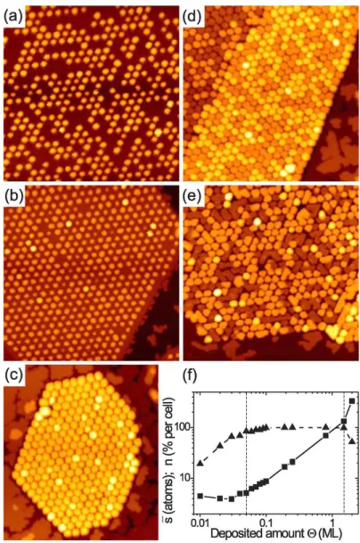
Figure 2.8 Cluster lattices on graphene flakes. The Ir coverages are (a) 0.03, (b) 0.10, (c) 0.80, (d) 1.50, and (e) 2.00 ML, respectively. Image height is always 550 Å. (f) Filling factor n in percent clusters per moiré cell (triangles) and average cluster size in atoms ¯s versus deposited amount Θ in ML (squares). Lines are to guide the eye. Reproduction from [44].
We conclude this section by taking a closer look at the growth mode of Ir cluster on graphene/Ir(111). Figure2.8(a)-(e) shows a series of STM topographs obtained by increasing the deposited amount of Ir. The quantitative analysis [Fig.2.8(f)]
of the filling factor n and the average cluster size in atoms sav versus deposited amount Θ suggests three regimes of cluster growth [44]: (i) A nucleation regime where n increases nearly linearly with Θ, while sav is almost independent of the coverage. (ii) A growth regime for coverages 0.05 ≤ Θ ≤ 1.50 ML in which n is
close or equal to one while the average cluster size increases proportionally with Θ.
(iii) A coalescence or sintering regime for Θ ≥ 1.50 ML, which is characterized by the onset of cluster coalescence. The coalesced clusters extend typically over several unit cells [Fig.2.8(e)]. In Chapter 5a similar study for Pt clusters is presented and their growth mode will be compared to that of Ir clusters.
2.3 Electronic Structure of Graphene
012 032 042
Figure 2.9 (a) Brillouin zone of the graphene honeycomb lattice. The Dirac cones are located at the K and K’ points (called Dirac points). (b) Electronic dispersion of graphene (π and π? bands) over the first Brillouin zone. The bands cross the Fermi level at the Dirac points. (c) Zoom of the energy bands close to one of the Dirac points. Reproduced from [99].
Graphene shows a number of interesting electronic effects [1, 3], which originate from its particular band structure (Fig.2.9). The occupied π and the unoccupied π? touch at the Fermi levelEF at the K-points of the first Brillouin zone, where the density of states vanishes [99] - the so-called Dirac points. As the density of states is zero at EF, graphene is often referred to as a ’zero gap semiconductor’. The bands show a linear dispersion around EF so that the dispersion resembles two touching cones. They are referred to as Dirac cones and are the electronic signature feature of graphene.
The electronic structure of graphene may, however, be altered by its support. This is especially the case for graphene supported by metal surfaces like Ni(111) or Ru(0001). On both surfaces, graphene is bound strongly through hybridization of graphene states with those of the metal [100, 101]. On the contrary, weakly in- teracting metal surfaces like Pt(111) or Ir(111) show but a little disturbance of the
2.3 Electronic Structure of Graphene 17 electronic structure of graphene [102, 103]. For the case of graphene/Ir(111) this is demonstrated in Fig.2.10.
Figure 2.10 (a) ARPES spectrum of clean Ir(111) taken φ = 0.5◦ ± 0.1◦ off the Γ-M direction. The positions of the K points of iridium and graphene are marked as KIr and Kg, respectively. S1 - S3 are surface states. (b) ARPES spectrum of Ir(111) covered by graphene along the same azimuth as in (a). Horizontal arrows denote minigaps in the primary Dirac cone. A visible replica band is labeled R. Reproduced from [103].
Figure 2.10(a) shows the ARPES spectrum of the clean Ir(111) surface [103]. Con- veniently, the region where the graphene Dirac cone is expected, coincides with an energy gap in the Ir(111) electronic structure. Only three weakly dispersing surface states exist in this gap. Figure2.10(b) shows the spectrum for graphene on Ir(111).
The linear branches of the Dirac cone are clearly visible. We can identify only faint substrate related features in the spectrum: A marginal doping of 0.10 eV, additional replica bands and the opening of minigaps. The latter two can be attributed to the periodic potential created by the moiré superstructure. Altogether, the band structure strongly resembles that of freestanding graphene (compare Fig.2.9(c)) and shows no sign of hybridization with substrate electronic bands.
The doping of graphene and how it can be tailored by intercalation will be the topic of Chapter 8. Another way to engineer the band structure of graphene/Ir(111) will be described in the following: Rusponi et al. [104] demonstrated that an Ir cluster lattice grown on the moiré pattern (as described in Section 2.2) gives rise to the opening of a band gap Egap. Figure2.11(a) shows an ARPES spectrum of graphene on Ir(111). This spectrum is similar to the one in Fig.2.10(b) except for the fact that a small band gap is observed at the Fermi level. As the unoccupied π? band is not visible in ARPES, only a lower limit of Egap can be estimated:
Egap,gr/Ir(111) ≥ 70 meV. Figure.2.11(b) shows that the cluster lattice noticeably enlarges the graphene band gap toEgap,Ir/gr/Ir(111) ≥200 meV. The question whether a band gap occurs upon cluster growth is, however, beyond the scope of this thesis.
Nevertheless, Rusponi et al. report that upon cluster deposition the C 1s core and the top of the σ band both shift 30 meV to higher binding energies (Fig.2.12). They conclude that the Dirac point ED also shifts by the same amount - a fact that will be considered in Section 8.2.
A feature, which Rusponi and coworkers do not address, is that the C 1s peak becomes asymmetric after cluster growth [red curve in Fig.2.12(a)]. A shoulder develops at the high binding energy side of the peak. The origin of this shoulder will be discussed in detail in Chapter 4.
Figure 2.11 (a) ARPES intensity of the π band of graphene on Ir(111), close to the K point, along the pΓK and the ΓK directions. A linear dispersion is observed along both directions. (b) ARPES intensity of the π band of graphene after growth of Ir clusters on graphene/Ir(111) along the same two directions. In (a) and (b) the dots represent the result of fitting the momentum distribution curves (MDCs). Note that the enlargement of the band gap is accompanied by an enhancement of the anisotropy in the energy dispersion of the Dirac cones. Reproduced from [104].
2.3 Electronic Structure of Graphene 19
012
032
Figure 2.12 (a) C 1s core levels for clean graphene (black) and after deposition of 0.15
±0.05 ML Ir (red). Inset: Zoom on the C 1s peak showing a shift of 30 ± 30 meV after cluster growth (normal emission, photon energy 450 eV). (b) Energy distribution spectra corresponding to the situations in (a). Measured at the M point of the second Brillouin zone. Inset: The top of theσ-band shifts by 30±30 meV after cluster growth. Reproduced from [104].
2.4 Intercalation of Graphene
Graphene Substrate Intercalant
Figure 2.13Schematic illustration of graphene before (upper panel) and after intercalation of atoms between the graphene layer and the substrate (lower panel). Redrawn from [66].
Intercalation refers to the insertion of molecules, atoms or ions into a chemical com- pound. Well known examples are graphite intercalation compounds [105, 106]. In the case of graphene, intercalation signifies the insertion of an adlayer of molecules or atoms between the graphene sheet and its substrate. This is sketched in Figure 2.13: The upper panel shows a pristine graphene layer on a substrate. The graphene is slightly corrugated which is typical for graphene supported by a weakly interact- ing, lattice-mismatched transition metal surface (compare Fig.2.2). The lower panel shows a layer of adatoms intercalated between the graphene sheet and the substrate.
As depicted, the adlayer may reduce the corrugation of the graphene layer by pas- sivating the substrate surface. This is one example how intercalation might affect the properties of graphene. Another example will be given in the following.
2.4 Intercalation of Graphene 21
0124567809992 0245667809992
7809992 7809992
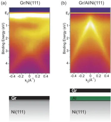
Figure 2.14ARPES intensity maps around the K-point along the direction perpendicular to Γ-K in the Brillouin zone for (a) graphene/Ni(111) and (b) the graphene/Al/Ni(111) system. Reproduced from [72].
Figure 2.14(a) shows the ARPES spectrum of graphene on Ni(111). We note that the original electronic structure of the free-standing graphene is strongly perturbed.
The Dirac cone is heavily distorted and graphene-derived electronic bands are shifted to higher binding energies [72]. The reason is that graphene is strongly bound to the Ni surface by hybridization of the graphene π and Ni 3d states [100,107, 108].
Figure 2.14(b) shows the ARPES spectrum after intercalation of Al between the graphene layer and the Ni surface. Contrary to the graphene/Ni(111) system, the Dirac cone is fully restored. After Al intercalation, the electronic structure resembles that of the free-standing graphene. Evidently, the Al layer effectively decouples graphene from the substrate. In addition, electron doping shifts the Dirac point belowEF by 0.64 eV. Doping of graphene by an intercalated layer will be discussed in detail in Chapter 8.
01231246278497
711227219
1
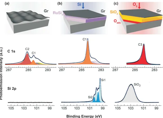
Figure 2.15 Step of SiO2 synthesis under epitaxial graphene on Ru(0001). (a) Formation of epitaxial graphene. (b) Exposure of the sample surface to silicon at 720 K. Si intercalates and forms a silicide with the metal substrate. (c) The metal silicide is oxidized to form an insulating SiO2 layer that separates the metal from graphene (pO2 = 4×10⁻³mbar, 640 K). The metal surface is terminated with chemisorbed oxygen. Schematics (upper panel) as well as photoemsision spectra from C 1s (middle panel) and Si 2p (lower panel) respectively. Note that the C 1s signal and that of the Ru 3d3/2(minor components in the middle panel) overlap energetically in the XPS spectrum. Modified from [77].
For most technological applications, graphene has to be supported by an insulator, or at least by an insulating layer. In order to use graphene grown on metals, one possibility is to transfer it from the metal onto the desired substrate. In this context, it was shown that Br2 intercalation is an efficient method to enable exfoliation of graphene grown on Ir(111) by adhesive tape [14].
Going one step further, Lizzit et al. developed a process which inserts an insulating layer in between the graphene sheet and the metal substrate [77]. It is sketched in Figure 2.15.
Firstly, graphene is prepared by epitaxial growth on Ru(0001) [Fig.2.15(a)]. The corresponding C 1s core level spectrum shows two peaks (C1 and C2). C2 arises
2.4 Intercalation of Graphene 23 from the strong coupling of the graphene layer to the Ru surface in parts of the moiré unit cell, C1 is the signature of the nonbonding parts (compare Fig.2.2 and [87]).
The additional minor components visible in the spectrum stem from photoemisson of the Ru 3d3/2 orbital.
Secondly, the sample surface is exposed to silicon under conditions allowing for in- tercalation [Fig.2.15(b)]. The C 1s spectrum consists of a single narrow component C1 signaling that the graphene layer is decoupled from the substrate. The Si 2p core level (as well as the Ru 3d, data not shown) indicates that the intercalated Si forms a silicide with the metal substrate. The total quantity of intercalated silicon atoms can be varied by adjusting the Si exposure time. Here, the Si coverage corresponds to approximately 4 ML.
Finally, the sample is exposed to O2: Oxygen intercalates below graphene and pro- gressively oxidizes the silicide layer. During oxidation, the silicide is consumed and the Si 2p spectrum transforms into a broad peak at higher binding energy, indicative of Si in SiO2 environment. The C 1s intensity converts into the single and narrow C3 peak, interpreted as graphene supported by SiO2. The C 1s spectrum does not show any sign of oxidation, demonstrating that graphene does not react with O2 during intercalation, and that during decomposition of the Ru silicide, oxygen binds exclusively to silicon.
By using a nanoscale four-point probe technique, the authors showed that the SiO2 layer provides electrical insulation of the graphene layer against the metallic sub- strate.
3 Experimental
All experiments described in this thesis were performed in ultra-high vacuum (UHV).
They were carried out in two laboratories: STM was done in the TuMA III labo- ratory at the Institute of Physics II at the University of Cologne, XPS was done at beamline I311 of the MAX IV Laboratory in Lund, Sweden. Both setups will be described briefly. An introduction to XPS is given and illustrated by several examples.
3.1 The Ultra High Vacuum System TuMA III
0
Figure 3.1 TuMA III UHV system [(a) sideview, (b),(c) cross sections]: (1) STM, (2) Ir(111) sample, (3) cooling reservoir, (4) Faraday cup, (5) manipulator, (6) e-beam evap- orator, (7) ion gun, (8) mass spectrometer with Feulner cup, (9) gas doser, (10) LEED system, (11,12) turbo molecular pumps, (13) ion pump, (14) cooling trap, (15) titanium sublimation pump. Figure modified from [109].
STM experiments were performed in the variable temperature UHV system TuMA III with a base pressure of 10−10mbar. Several pumps are used to achieve such a
25
low pressure: a turbomolecular pump, an ion pump, a titanium sublimation pump and a cooling trap on the main chamber as well as a second turbomolecular pump for differential pumping of the ion gun.
The STM is of the beetle type with a homemade Ir tip. Low-energy electron diffrac- tion (LEED) is used to determine the surface structure. The quadrupole mass spec- trometer (QMS) is used for residual gas analysis as well as for thermal desorption spectroscopy (TDS). To obtain a better signal to noise ratio in TDS measurements the mass spectrometer was equipped with a Feulner cup in the course of this thesis [110].
The sample used for all experiments is an iridium single crystal with an (111) ori- ented surface which is mounted in a transferable and rotatable manipulator. The sample is heated by electron bombardment and is connected to a liquid nitrogen reservoir for cooling. The temperature is measured by a type K (chromel-alumel) thermocouple.
The system is further equipped with an ion gun including a mass filter and a Faraday cup to measure the ion flux. A gas dosing system is used to dose gases in proximity of the sample. The local pressure in front of the gas doser was estimated to be 80 times higher than the measured pressure of the chamber [109]. Pressures given in this thesis always refer to the local pressure at the sample.
A four pocket e-beam evaporator (EGN4, Oxford Applied Research) is used for metal deposition. It is equipped with a manual shutter and an ion flux monitor.
Typical evaporation rates are e.g. 3×10⁻² ML/s for the evaporation of Pt. During evaporation the pressure remained in the low 10−10 mbar range.
A detailed description of the TuMA III setup is given in [111].
3.2 Principle of X-ray Photoemission Spectroscopy 27
3.2 Principle of X-ray Photoemission Spectroscopy
In this section the principle of XPS and its experimental realization is described.
Peculiarities of the beamline I311 are described in the next section.
01023456
Figure 3.2Principle of photoemission spectroscopy. Monochromatic photons with energy hνare produced by a light source and hit the sample surface under an angleΨwith respect to the surface normal. The kinetic energyEkin of the photoelectrons can be analyzed by use of electrostatic analyzers (usually by an additional retarding field) as a function of the experimental parameters. The whole setup is evacuated to ultra high vacuum (UHV) (from [112]).
XPS is a surface sensitive technique used to investigate the composition of a sample and the chemical state of the constituting atoms. The principle of photoemission spectroscopy (PES) is shown in Figure 6.5. Monochromatic light – which can be either generated by a lab source (e.g. Al-Kα X-ray anode) or preferably by a syn- chrotron radiation facility – is directed onto the sample. If the energy of the light is in the X-ray regime (100 eV to 10 keV), the technique is referred to as X-ray photo- emission spectroscopy (XPS). Due to the photoelectric effect the impinging photons create photoelectrons with an kinetic energyEkin of
Ekin =hν−φ−EB (3.1)
wherehνis the photon energy,φthe work function of the sample, andEBthe binding energy of the electron in the sample. The kinetic energy Ekin of the photoelectron is typically measured by using hemispherical analyzers. The analyzer is usually operated in the fixed transmission mode. This means that the photoelectrons are decelerated by a retarding voltage and pass the hemisphere with a constant kinetic
Figure 3.3 Schematic view of the photoemission process. Electrons with binding energy EB can be excited above the vacuum level Evac by photons with energy hν > EB + Φ0. The photoelectron distribution I(Ekin) can be measured by the analyzer and is (in first order) an image of the occupied density of electronic states N(EB) in the sample. The discrete core level states of the sample give rise to peaks of a finite width in the spectrum.
Note that also the Fermi level is also broadened. (from [112])
energy (the so-called pass energy). A spectrum over an energy range is obtained by varying the retarding voltage. The quantity of interest is the binding energy EB, which can in principle be calculated with the help of Eq.3.1once the kinetic energy of the photoelectrons EBis measured. For this calculation the photon energyhνand the work function φhave to be known very precisely. It is therefore more convenient to calibrate the binding energy scale directly to the Fermi energy EF (see Fig. 3.3).
A schematic view of the photoemission process is given in the energy diagram shown in Fig. 3.3. This simplified picture shows the purpose of photoemission spectroscopy:
the properties of the photoelectrons basically reflect the electronic structure of the investigated system [112]. The discrete core level states of the sample give rise to peaks of a finite width in the spectrum. The peak positions are defined by electron
3.2 Principle of X-ray Photoemission Spectroscopy 29 binding energies which are characteristic for the atomic species under investigation.
In other words the presence of a peak at a certain binding energy is a sign for the presence of a certain element in the sample. Photoemission spectroscopy can therefore be used to investigate the composition of a sample. However, XPS is a much more powerful tool: It is not only able to reveal the composition of the sample but also the chemical bonding state of the atoms in the sample. The latter is due to the fact that core level binding energies vary depending on the chemical environment of the atom. These variations are called chemical shifts or core level shifts. An overview of the theory and of various approaches to the interpretation of core level shifts can be found in the review by Egelhoff [113].
The surface sensitivity of XPS is due to the mean free path of the photoelectrons (Fig. 3.4). For kinetic energies of around 100 eV the mean free path is of the order of only a few Å. If measurements are performed at a synchrotron facility, the user can tune the energy hν of the photons to a value that the kinetic energy of the photoelectrons becomes Ekin ≈ 100 eV so that a maximum of surface sensitivity is achieved. This is done by setting hν to the binding energy EB of the core level under investigation plus ∼100 eV (compare Eq. 3.1). For example we have chosen a photon energy of 390 eV to investigate the carbon 1s core level that has a binding energy ofEB,C 1s ≈ 284 eV (compare Section3.4). We will see below that - with the appropriate photon energy - the XPS signal originating from the surface of our Ir crystal equals the signal originating from the bulk of the Ir crystal in intensity.
Figure 3.4 Mean free path of excited electrons in solids against kinetic energy. This so- calleduniversal curve shows a minimum of approximately 5 Å at 20 - 100 eV kinetic energy (Figure from [114], original data from [115]).
3.3 The Beamline I311 at Max-lab
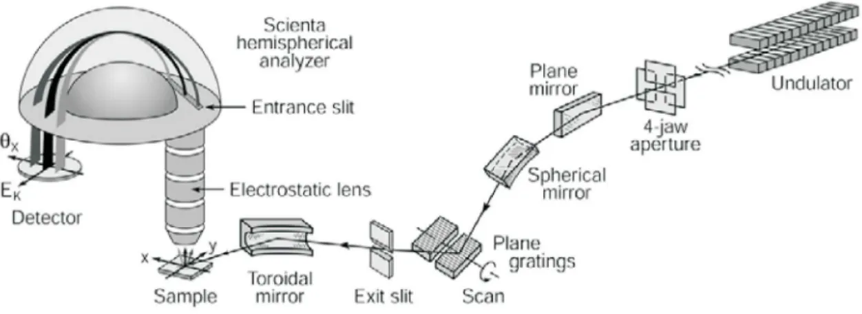
XPS measurements were carried out at beamline I311 of the MAX II storage ring of the MAX IV Laboratory in Lund, Sweden. MAX II is a third generation syn- chrotron source with a circumference of 90 m and a maximum stored current of 300 mA [116]. Inside the storage ring electrons are accelerated until they reach an energy of 1500 MeV. At this energy the electrons have a speed of 99.99999 % of the speed of light. Bending magnets, wigglers, and undulators are used to generate photons in the X-ray regime by deflecting the electrons in a magnetic field.
I311 is an undulator based soft X-ray beamline with two end stations: One dedicated to XPS and NEXAFS, the other used for LEEM and PEEM measurements. Figure 3.5 shows a sketch of a typical beamline setup for XPS measurements.
Figure 3.5 Sketch of a typical beamline setup for XPS measurements including (among others) an undulator, a plane grating monochromator, an exit slit behind the grating, and an entrance slit in front of the analyzer, the sample and a detector as well as several mirrors and lenses (from [114]).
Photoemission spectroscopy requires monochromatic X-rays of a certain energy (see Section 3.2 for how this energy is selected to achieve a maximum of surface sensi- tivity). However, the undulator emits light of a characteristic spectrum depending on the undulator gap [Fig. 3.6 (b)]. This gap is tuned to maximize the intensity of the light at the desired photon energy.
3.3 The Beamline I311 at Max-lab 31
0 123
5123667
898 8 9 8 9 8
157
8 98
527
527
5!7
Figure 3.6(a) Principle of an undulator. Permanent magnets (1) seperated by a tunable gap generate a static magnetic alternating along the length of the undulator with a wave- length λu. The electrons (2) traversing the periodic magnet field are forced to undergo oscillations and radiate (3). (from [117])
(b) Photon energy spectra generated by the undulator at I311 for different settings of the gap (from [116]). Note that for small gaps the undulator mimics the behaviour of a wiggler, giving high output with only weak undulator features over a large photon energy.
Afterwards the light is monochromated by an optical grating (Zeiss SX-700, 1220 lines/mm) and passes an adjustable exit slit. Fig. 3.7 displays the resolution of the grating as a function of photon energy for different settings of the slit. It is evident that for a given photon energy the resolution can be improved by narrowing the exit slit. However, a reduction of the slit size also reduces the number of photons reaching the sample so that measuring time is increased. A compromise must be found for each spectrum.
011 0111 0
01 011 0111
23456784934
32345674
11 01 011 1 1
Figure 3.7 Energy resolution of the Zeiss SX-700 grating at I311 as a function of photon energy for different settings of the exit slit (modified from [116]).
The light is focused by mirrors onto the grating and from there onto the sample.
The spot size on the sample is about 0.5 mm horizontally and 0.1 mm vertically, thus the area that is probed is 0.05 mm2. The exited photoelectrons are analyzed by a hemispherical Scienta SES200 Analyzer and detected by a CCD camera. The analyzer is operated in the fixed analyzer transmission mode. The energy resolution of the analyzer is given by
Res(eV) = Epass·s 2R
where s is the width of the entrance slit of the analyzer and R its radius (200mm).
The resolution can be improved by reducing the width of the entrance slit or the pass energy on the expense of intensity. A balance between intensity and resolution has to be found.
3.4 Experimental Procedures and Calculations 33
3.4 Experimental Procedures and Calculations
The Ir(111) crystal was cleaned by cycles of Ar+ (XPS) or Xe+ (STM) sputtering at room temperature with subsequent O2 treatment at 1200 K (1×10⁻⁷ mbar, 10 min), followed by vacuum annealing to above 1400 K. No subsurface Ar gas bubbles were observed with STM.
The growth of partial graphene layers with 0.2 ML, 0.5 ML or 0.95 ML coverage was performed by 1, 3 or 10 cycles of ethylene (C2H4) adsorption till saturation at room temperature followed by thermal decomposition at 1400 K [44, 86, 118]. 1 ML (monolayer) graphene corresponds here to full coverage of the Ir(111) substrate.
The resulting 0.5 ML graphene layer is not yet percolated and consists of flakes and coalesced flakes with a broad size distribution with circle equivalent (CE) diame- ters of 10 nm to 100 nm. The 0.95 ML graphene layer is percolated and displays uncovered Ir(111) patches at distances of the order of micrometers in STM.
The perfectly closed 1 ML graphene layer was grown by one cycle of adsorption and thermal decomposition followed by chemical vapor deposition of ethylene (p = 1×10⁻⁷ mbar) for 2400 s at 1170 K [13]. Graphene layers of comparable quality can also be achieved by CVD alone if the growth temperature is chosen high enough [83]. We dismissed the latter method as it would require prolonged sample heating.
For all graphene coverages these growth recipes only yield the well-known incommen- surate (9.32 x 9.32) moiré superstructure with the dense packed rows of graphene and Ir(111) in parallel with a scatter of less than±0.5◦ [86]. Consequently, the film displays no graphene edge atoms and only a marginal concentration of point defects, which accommodate the small tilts. The quality and uniqueness of orientation of the prepared graphene and the absence of differently oriented domains was checked by LEED in both the STM and the XPS chamber. In the XPS chamber the absence of CO adsorption at room temperature confirmed the closure of the 1 ML graphene layer. In the STM chamber the full coverage with graphene was directly confirmed by low magnification STM imaging all over the sample.
High purity metals (Pt, Ir, Au) were sublimated with a commercial e-beam evapo- rator, resulting in a typical deposition rate of e.g. 3×10⁻² ML/s for Pt. Coverages are defined, such that 1 ML corresponds to the surface atomic density of Ir(111).
During deposition the sample was kept at 300 K if not indicated otherwise, and the pressure remained in the low 10−10 mbar range. The evaporator was calibrated in the STM chamber by determination of the fractional area of monolayer metal is-
lands deposited onto clean Ir(111). At the I311 beamline the same evaporator as in the TuMA-III Lab was used with identical settings and distance to the sample. For Pt evaporation the STM rate calibration was confirmed in the XPS setup using the Ir 4f surface peak which vanishes at 1 ML coverage. Both calibrations agree within 10 %.
STM imaging was conducted at room temperature if not indicated otherwise. STM topographs were post-processed using the WSxM software [119]. Tunneling resis- tances of ≈ 2×10¹⁰Ω are used to avoid tip-cluster interaction. Moreover, owing to the convolution of the tip shape with the clusters, multilayered clusters tend to display a larger base area compared to 1-layered ones.
All XP-spectra were collected in normal emission. If not specified otherwise, all spectra are taken with photon energies of 190 eV for Ir 4f, Pt 4f, and Au 4f, 390 eV for C 1s, and 650 eV for O 1s, respectively. The total energy resolution of the light and analyzer is better than 45 meV, 60 meV and 200 meV for the respective core level spectra. The spectra were fitted with Doniach-Sunjic (DS) functions [120]
convoluted with Gaussians. The parametersα and the Lorentzian full width at half maximum (LFWHM) of the DS functions account for the asymmetry of the peaks, due to inelastic scattering of photoelectrons, and for the finite lifetime of the core hole, respectively. The Gaussian full width at half maximum (GFWHM) accounts for the experimental broadening. A linear background was used for the curve fitting.
All spectra are normalized to the background, and core binding energies, defined to have positive values, are referenced to the Fermi edge. Accordingly, a positive core level shift (CLS) corresponds to a binding energy increase.
Density functional theory (DFT) calculations were done by Peter J. Feibelman in order to optimize structures and to calculate core level shifts. Calculated core- level shifts were obtained in the fully-screened hole approximation, in which the total energy of the system plus core hole is computed by setting the core potential of the ionized atom to that of the same atom with the appropriate core electron missing. Total energies were evaluated using the VASP DFT code [121, 122], with a LDA Functional, based on the Ceperley-Alder Local Density Functional [123], as parametrized by [124], in the Projector Augmented Wave (PAW) Approximation [125, 126]. The LDA Functional was chosen for the present work since it describes the binding of Ir islands on graphene better than the PW91-GGA Functional [79].
As in Ref. [79], graphene/Ir(111) was modeled as a 10×10 graphene adlayer on the
3.4 Experimental Procedures and Calculations 35 upper surface of a 9×9, 4-layer, Ir(111) crystalline slab. This is a very good approxi- mation to the experimentally observed incommensurate 10.3×10.3 graphene layer on a 9.3×9.3 substrate mesh. In structural optimizations, with and without overlying Pt islands, the atoms of the bottom Ir layer were fixed in a (111) bulk, crystal plane, with an Ir-Ir nearest neighbor distance equal to 2.701 Å, the theoretical optimum.
Positions of all remaining atoms were relaxed until none experienced a force of mag- nitude > 45 meV/Å. Electronic relaxation was accelerated using Methfessel-Paxton Fermi-level smearing (width = 0.2 eV) [127], and corrected for the unphysical con- tact potential difference associated with having a graphene adlayer on one side of the Ir slab only [128]. A 400 eV plane-wave basis cutoff was used as well as a 3×3 surface brillouin zone sample for the sake of good accuracy.
4 How Pt Clusters Bind to the Graphene Moiré on Ir(111)
The results of this chapter (except Section 4.3) are published in Physical Review B 85, 035407 (2012) [84]. I was strongly involved in the XPS
measurements and conducted the STM experiments. I was involved in
discussion and analysis of the data as well as in commenting and editing of the manuscript. Section 4.3 was added by myself.
In Section2.2 the DFT based scenario of cluster binding to the graphene moiré was described [79, 80]. Despite its plausibility, there is as yet no experimental evidence for the rehybridization picture beyond agreement of the experimentally-determined binding site preference of the metal clusters with what DFT calculations predict. A way to proceed is suggested by previous investigations of the binding of graphene to different metals [87, 129] and of how differently sized graphene flakes bind to the Ir(111) substrate [90]. In this chapter, we will show XPS measurements of C 1s core level shifts for graphene/Ir(111) with and without adsorbed clusters present, and we compare them to calculated shifts based on the rehybridization picture.
To set a standard for agreement between DFT theory and XPS data, we will first compare measured and calculated C 1s CLS of graphene on Ir(111) without adclus- ters (Section4.1). The effect of cluster adsorption is the subject of Sections4.2 -4.4, where we analyze experimental and calculated results of the C 1s CLS of graphene with Pt adclusters, and of the Pt 4f7/2 CLS of the adsorbed clusters themselves.
Further, we present Ir 4f spectra showing a signature of graphene interaction with the Ir surface.
37
4.1 A Test Case: Core Level Spectrum of Pristine Gr/Ir(111)
Figure 4.1(a) shows an STM topograph of graphene on Ir(111) with the moiré unit cell indicated. Both the honeycomb structure formed by the carbon atoms and the moiré’s different high symmetry domains are visible. The latter are labeled top, hcp or fcc according to the position of the center of the carbon rings [44]. A ball model of the DFT optimized structure in Fig.4.1(b) shows the geometry of the high symmetry domains and the undulation of the graphene. C-atoms in top domains reside 3.85 Å above the Ir surface, whereas those in hcp/fcc domains lie about 0.6 Å lower. The C-atoms are grouped in Fig.4.1(b) according to their height and binding geometry. Those in threefold hollow sites are labeled by and 4, in bridge sites by and in atop sites by ◦ and ..
To understand how the graphene-Ir(111) distance and the local geometry of C-atoms affect the C 1s core level we calculated the CLS of the 200 C-atoms in the moiré unit cell using the core ionization potential of a C-atom in a isolated graphene layer as a reference. The results are shown in Fig. 4.1(c) using the same colored symbols as in Fig. 4.1(b) to distinguish atoms at different heights and adsorption sites. Com- paring C-atoms in threefold hollow [ and 4 in Figs. 4.1(b-c)] or bridge sites [ in Figs. 4.1(b-c)] it is clear that there is an approximate linear correlation between the graphene-Ir(111) distance and the C 1s core level binding energy, which is lower for atoms farther from the substrate. Core shifts estimated in the initial state approxi- mation [113], which are the main contributions to the numbers we calculated, offer insight into the sign of this effect. The key idea is that CLS’s are more negative on atoms that gain electronic charge, and more positive on those that lose it. Thus, the CLS’s on C atoms farther from the metal imply that they are somewhat negatively charged, while the atoms that lie lowest are positive. This charge redistribution is consistent with an electrostatic interaction between the mobile electrons of the graphene and the electron spillout charge of the underlying metal. That is, the positive charge of the low-lying moiré regions is favorable by virtue of attraction to the metal’s spillout electrons. Equally, the negative charge of the high-lying regions is favorable by virtue of repulsion from them.
Although this explanation of the CLS’s is convincing we want to offer an alternative interpretation. A consequence of charge transfer to or from the graphene layer is
4.1 A Test Case: Core Level Spectrum of Pristine Gr/Ir(111) 39
Height [Å]
HCP FCC
TOP TOP
Intensity (a.u.)
(d)
TOP FCCHCP
(a)
(b)
2.5 3.5 3.0
Height (Å) -0.4
-0.3
C1s CLS (eV)
3.2 3.4 Height (Å)3.6 3.8
HCP
(c)
BE (eV)
284.6 284.4 284.2 284.0 283.8 283.6
Figure 4.1 (a) STM topograph (59×84 Å2, U= 1V, I=7nA) of the graphene moiré on Ir(111). The three high symmetry domains top, fcc and hcp are indicated. (b) Schematic illustration of the DFT optimized C(10×10)/Ir(9×9) moiré unit cell showing a top view, and a side view along the unit cell diagonal. The height of the C atoms is given by the color scale. The C-atoms in threefold hollow sites are labeled by and 4, in bridge sites by and in atop sites by ◦ and . (see text). (c) Calculated C 1s CLS for the 200 atoms in the moiré unit cell. (d) Black dots represent the experimental C 1s spectrum. The gray curve is the superposition of 200 peaks with a binding energy distribution according to the DFT calculated CLS. The 5 colored components are the sums of peaks originating from C atoms marked with,4,,◦, and. in panel (b), respectively.