Surface Acoustic Waves in Strain-Engineered Thin (K,Na)NbO 3 Films:
From Basic Research to Application in Molecular Sensing
Inaugural-Dissertation zur
Erlangung des Doktorgrades
der Mathematisch-Naturwissenschaftlichen Fakultät der Universität zu Köln
vorgelegt von
Sijia Liang
aus Henan, PR China
Jülich, 2021
Berichterstatter: Prof. Dr. Roger Wördenweber Prof. Dr. Markus Grüninger Prof. Dr. Joachim Hemberger
Tag der mündlichen Prüfung: Feb. 16, 2021
I
Zusammenfassung
In dieser Arbeit zeigen wir, dass in Dünnschichtsystemen die Energie der akustischen Oberflächenwellen (SAW) im Vergleich zu kompakten Bulksystemen wesentlich stärker auf der Oberfläche konzentriert ist, wodurch diese Systeme äußerst empfindlich auf Störungen an der Oberfläche reagieren. Auf dieser Basis haben wir ein Dünnschicht-SAW-Sensorsystem mit extrem hoher Empfindlichkeit für Massenbelegung entwickelt. Aufgrund seiner hervorragenden piezoelektrischen Eigenschaften wurde K
xNa
1-xNbO
3(KNN) als Kandidat für das Dünnschichtsystem ausgewählt. Unter Verwendung epitaktischer Verspannung wurden die piezoelektrischen Eigenschaften angepasst, um das SAW-Signal und die Empfindlichkeit der Schicht zu verbessern. Abschließend wurde ein SAW-Sensor auf der Basis extrem dünner (~ 30 nm) KNN Filme entwickelt, mit dem die Abscheidung von Monolagen organischer Moleküle erfasst werden konnte.
Für die Abscheidung von epitaktischen KNN-Filmen wurden zwei Methoden verwendet - metallorganische chemische Gasphasenabscheidung (MOCVD) und gepulste Laserabscheidung (PLD). Eine Reihe unterschiedlicher Scandate (DyScO
3(DSO), TbScO
3(TSO), GdScO
3(GSO) und SmScO
3(SSO)) wurden als Substrate mit unterschiedlichen Gitterfehlanpassungen in Bezug auf die KNN-Filme und daher unterschiedlichen Niveaus der Verspannung ausgewählt. Gemäß Röntgenanalyse (ins.reziproke Raumkartierung (RSM)) zeigen die MOCVD-präparierten KNN-Proben ein perfektes epitaktisches Wachstum, während die PLD-präparierten Proben zwar epitaktisch sind, aber eine beginnende plastische Relaxation zeigen. Als Folge dessen zeigen die MOCVD-Proben das typisches konventionelle ferroelektrische Verhalten ohne merkliche Frequenzdispersion des ferroelektrischen Phasenübergangs, während die PLD-Proben ein lehrbuchartiges Relaxorverhalten mit einem frequenzdispersiven ferroelektrischen Phasenübergang zeigen. Es scheint, dass die höhere Teilchenenergie der PLD zu Inhomogenitäten der mikroskopischen Zusammensetzung führt, die die Bildung polarer Nanoregionen (PNR) nach sich zieht.
Aufgrund der kompressiven Verspannung werden die Phasenübergangstemperaturen der
MOCVD- und PLD-Proben von T
C≈ 693 K für unverspanntes KNN zu niedrigeren Temperaturen
verschoben. Zunächst wird ein „quadratisches Modell“ angewendet, um die
Dehnungsabhängigkeit der Phasenübergangstemperatur zu analysieren. Die Phasenüber-
gangstemperaturen von MOCVD-Proben zeigen eine perfekte lineare Abhängigkeit von der
Druckspannung, während die PLD-Proben keine klare Abhängigkeit zeigen. Um das Modell zu
verbessern, wird ein „vertikales Gittermodell“ (VLM) vorgeschlagen, das auf dem Poisson-
Effekt basiert. Im neuen Modell wird die Dehnung der Filme durch den vertikalen
Gitterparameter des KNN-Films dargestellt. Die Phasenübergangstemperaturen von MOCVD-
und PLD-Proben zeigen nun eine perfekte lineare Abhängigkeit vom vertikalen
Gitterparameter mit leicht unterschiedlichen Steigungen für MOCVD und PLD. Dies bestätigt
II
das neue VLM Modells zur Beschreibung der Verspannungsabhängigkeit der Phasenübergangstemperatur.
Die dielektrischen Eigenschaften der verspannten KNN-Filmen sind stark verbessert. Z.B.
ergibt sich eine maximale Permittivität von 𝜀
𝑚𝑎𝑥′≈ 13695 bei ~ 330 K und eine Raumtemperatur (RT) Permittivität von 𝜀
𝑅𝑇′≈ 5166 für einen 27 nm dicken K
0.7Na
0.3NbO
3-Film auf TSO, hergestellt durch MOCVD, im Vergleich zu 𝜀
𝑚𝑎𝑥′≈ 6400 und 𝜀
𝑅𝑇′≈ 600 für unverspanntes KNN. Weiterhin sind die dielektrischen Eigenschaften anisotrop, z.B. ist das Verhältnis der RT-Permittivität gemessen entlang der beide TSO-Hauptachsen 𝜀
[11′ ̅0]/𝜀
[001]′= 1.33.
Im nächsten Schritt wurden die SAW-Eigenschaften von MOCVD- und PLD-Proben untersucht.
Die MOCVD-Proben zeigen starke SAW-Signale bei RT (∆S
21bis ~ 4 dB), was sogar mit Bulk- SAW-Kandidaten vergleichbar ist. Darüber hinaus können höhere Harmonischer (lediglich ungerader Ordnung) erzeugt werden. Die 3. Harmonische zeigt die größte Intensität. Im Gegensatz dazu sind die SAW in PLD-Proben kaum sichtbar. Diese Situation ändert sich jedoch erheblich mit dem Anlegen einer Gleichstromvorspannung. Die SAW-Intensität steigt von ~ 0,2 dB für eine Vorspannung von Null auf ~ 4 dB für eine Gleichstromvorspannung von 40 V/mm. Die DC-Vorspannung ermöglicht so eine neuartige elektronische Abstimmung des SAW-Signals. Dies neuartige Verhalten lässt sich durch das Verhalten der PNRs der PLD-Proben erklären.
Schließlich wurde ein Gasphasen-SAW-Sensor auf der Basis der verspannten KNN- Dünnschichten entwickelt,. Der SAW-Sensor wurde erfolgreich zur in-situ Überwachung der molekularen Schichtabscheidung (MLD) eingesetzt. Eine extrem hohe Empfindlichkeit des Sensors konnte in diesen Experimenten nachgewiesen werden, sogar noch mit der Ordnung der SAW-Harmonischen zunimmt. Eine Empfindlichkeit von S
i≈ - 22,3 bis - 116,7 kHz/nm konnte abgeschätzt werden, was im Vergleich zur Empfindlichkeit von konventionellen Bulk- SAW-Sensoren eine um mindestens eine Größenordnung höhere Empfindlichkeit darstellt.
Unsere Arbeit demonstrieren die Möglichkeit, die Empfindlichkeit von SAW-Systemen durch
Verwendung extrem dünner, verspannte und piezoelektrischer Schichten enorm zu
verbessern. Die extrem hohe Empfindlichkeit, die in unserem Dünnschicht-SAW-System
gezeigt wurde, impliziert potenzielle Anwendungen, die von der In-situ-Detektion der
Monoschichtablagerung bis zur hochselektiven und sensitiven Erkennung biologischer Marker
für die Krankheitsdiagnostik (z.B. POCT) reichen.
III
Abstract
In this work we demonstrate that in thin film systems, the energy of surface acoustic waves (SAW) is more concentrated on the surface compared to bulk system, which makes this system extremely sensitive to any perturbation on the surface. On this basis we developed a thin film SAW system with extremely high sensitivity to any mass loading. Due to its outstanding piezoelectric properties, K
xNa
1-xNbO
3(KNN) was chosen as a candidate for the thin film system. Using epitaxial strain the piezoelectric properties were tailored in order to improve the SAW signal and sensitivity. Finally, a thin (~ 30 nm) film KNN based SAW sensor was developed which allows to detect monolayer deposition of organic molecules.
For the deposition of epitaxial KNN films, two methods—metal organic chemical vapor deposition (MOCVD) and pulsed laser deposition (PLD)—were used. A series of scandates, DyScO
3(DSO), TbScO
3(TSO), GdScO
3(GSO), and SmScO
3(SSO), were chosen as substrates with different lattice mismatch with respect to the KNN films and therefore different levels of compressive strain. According to X-ray analysis (reciprocal space mapping (RSM)), the MOCVD-prepared KNN samples show perfect epitaxial growth, whereas the PLD-prepared samples are epitaxy but show an onset of plastic relaxation. The MOCVD samples exhibit a typical conventional ferroelectric behavior with hardly any frequency dispersion of the ferroelectric phase transition. In contrast, the PLD samples show textbook-like relaxor behavior with a frequency dispersive ferroelectric phase transition. It seems that the higher particle energy of PLD leads to microscopic composition inhomogeneities which results in the formation of polar nanoregions (PNR).
Due to the compressive strain, the phase transition temperatures of MOCVD and PLD samples are shifted from T
C≈ 693 K for unstrained KNN to lower temperatures. A “square model” is first applied to analyze the strain dependence of the phase transition temperature. The phase transition temperatures of MOCVD samples show a perfect linear dependence on compressive strain, whereas the PLD samples show no clear dependence. In order to improve the model, a
“normal lattice model” (NLM) is proposed which is based on the Poisson effect. In the new model, the strain of the film is represented by the vertical lattice parameter of the KNN film.
The phase transition temperatures of both MOCVD and PLD samples show a perfect linearity with slightly different slopes as function of vertical lattice parameter. This supports the use of the new model for the description of the strain dependence of the phase transition temperature.
The dielectric properties of strained KNN films are highly improved, e.g. a maximum
permittivity of 𝜀
𝑚𝑎𝑥′≈ 13695 at ~ 330 K and a room temperature (RT) permittivity of 𝜀
𝑅𝑇′≈
5166 are achieved for a 27 nm-thick K
0.7Na
0.3NbO
3film on TSO prepared by MOCVD compared
to 𝜀
𝑚𝑎𝑥′≈ 6400 and 𝜀
𝑅𝑇′≈ 600 for unstrained KNN. Furthermore, the dielectric properties are
IV
anisotropic, e.g. the ratio of the permittivity measured along [11̅0]
TSOand [001]
TSOdirections is 𝜀
[11′̅0]/𝜀
[001]′= 1.33 for the MOCVD film on TSO.
In the next step, the SAW properties of MOCVD and PLD samples were investigated. The MOCVD samples show strong SAW signals at RT (∆S
21up to ~ 4 dB) which is even comparable to bulk SAW candidates. Moreover, high orders of odd harmonics can be generated and the 3
rdharmonic shows the largest intensity. In contrast, the SAW in PLD samples are hardly visible. However, this situation changes significantly with the application of a DC bias. The SAW intensity increases from ~ 0.2 dB for zero bias to ~ 4 dB for a DC bias of 40 V/mm. The DC bias allows an electronic tuning of the SAW signal. This explained by the relaxor-type behavior based on the PNRs of the PLD samples.
Finally, a gas-phase SAW sensor is developed based on KNN thin films. The SAW sensor has been successfully applied to in situ monitoring of molecular layer deposition (MLD). An extremely high sensitivity of the sensor has been demonstrated. This sensitivity even increases with the order of the SAW harmonic. A sensitivity of S
i≈ - 22.3 to - 116.7 KHz/nm is demonstrated. Compared to the sensitivity of SAW sensors based on bulk systems, the thin film SAW sensor system exhibits at least one order of magnitude higher sensitivity.
Our work provides a way of improving the sensitivity of SAW systems via applying thin films.
The extremely high sensitivity demonstrated in our thin film SAW system implies potential
applications ranging from in situ detection of monolayer deposition to highly selective and
sensitive sensing of biological markers for disease diagnosis (e.g. point-of-care-testing
(POCT)).
V
Contents
Zusammenfassung ... I Abstract ... III
1 Introduction ... 1
2 Theoretical background... 4
2.1 Fundamentals of ferroelectrics ... 4
2.1.1 Dielectricity... 5
2.1.2 Ferroelectricity ... 8
2.1.3 Ferroelectric phase transition ... 10
2.1.4 Piezoelectricity ... 11
2.2 Engineering of ferroelectricity ... 12
2.2.1 Doping ... 12
2.2.2 Strain ... 14
2.2.3 Relaxor ... 16
2.3 Surface acoustic waves ... 19
2.3.1 Surface acoustic wave modes ... 19
2.3.2 Generation and detection of surface acoustic waves ... 21
2.3.3 Surface acoustic waves sensors ... 25
2.4 Introduction to K
xNa
1-xNbO
3... 28
3 Sample preparation and experimental techniques... 30
3.1 Sample preparation ... 30
3.1.1 Metal organic chemical vapor deposition ... 30
3.1.2 Pulsed laser deposition ... 31
3.1.3 Evaporation deposition ... 32
3.1.4 Molecular layer deposition ... 32
3.2 Film characterization ... 33
3.2.1 High resolution X-ray diffraction ... 34
3.2.2 Reciprocal space mapping ... 35
3.2.3 Atomic force microscopy ... 37
3.2.4 Time-of-flight secondary ion mass spectroscopy ... 38
3.3 Electrodes fabrication ... 40
3.4 Electronic characterization ... 42
3.4.1 Temperature control ... 43
3.4.2 Permittivity measurement ... 44
3.4.3 Surface acoustic wave measurement ... 46
3.4.4 Surface acoustic wave sensor ... 47
4 Strain engineering of the ferroelectric properties of K
xNa
1-xNbO
3films ... 51
4.1 Structure, strain, and stoichiometry ... 51
VI
4.2 Strain engineering of T
C... 56
4.3 Strained conventional and relaxor-type ferroelectrics ... 62
4.4 Summary ... 66
5 SAW properties in conventional ferroelectric (K,Na)NbO
3... 67
5.1 SAW properties at room temperature ... 67
5.2 Impact of strain on SAW properties ... 76
5.3 Temperature dependence of permittivity and SAW signal ... 79
5.4 Summary ... 82
6 Tunable SAW properties of relaxor-type ferroelectric (K,Na)NbO
3... 84
6.1 SAW properties without dc bias ... 84
6.2 DC bias tuning of the SAW ... 90
6.3 PNR-model for DC bias tuning ... 94
6.4 Summary ... 98
7 KNN thin film gas-phase SAW sensor ... 99
7.1 MLD sensor system ... 99
7.2 SAW sensor operation at elevated MLD temperature ... 108
7.3 Summary ... 112
8 Conclusion ... 113
References ... 116
Appendix ... 123
Sample list ... 123
E-beam lithography and lift-off recipe ... 125
Acknowledgement... 127
1
1 Introduction
Due to their outstanding properties, surface acoustic wave (SAW) based devices are presently widely used in communications, signal processing, and transducer, actuator, and sensor techniques [1-6]. For example, the most common applications of SAWs are probably special filters in our smart phones, which make our daily life so comfortable. Maybe even more important are sensor applications which allow extremely sensitive detection of change in temperature, pressure, mechanical force and especially mass loading [7-10]. The latter is for example of interest for medical applications like the detection of bacteria or viruses. However, for the detection of many interesting biomarkers or pathogens even the sensitivity of existing SAW sensors is not good enough. The aim of this work is therefore to explore new way to improve the sensitivity of SAW sensor systems.
The working principle of SAW mass detector is based on the impact of the mass loading on the properties of the acoustic wave travelling at surface of the sensor. Since the SAW amplitude attenuates exponentially with depth into the material [11], the acoustic energy is concentrated at the surface and therefore sensitive to mechanical, chemical, optical or electrical perturbations of the surface.
First, one way to boost the sensitivity of a SAW sensor could be to confine the energy of the acoustic wave even more to the surface. Therefore, we decided to develop SAW sensor systems based on extremely thin piezoelectric films. Due to the thinness of these films, the acoustic energy of the propagating SAWs can be further concentrated on the surface, resulting in a highly increased energy density. Consequently, the SAWs generated in the thin films are more sensitive to surface perturbations and therefore possess an improved sensitivity.
Second, since most of the sensor systems are operated at or around room temperature (RT), materials with perfect piezoelectric properties around RT are required. The piezoelectric and thus SAW response is usually largest close to the phase transition temperature, which unfortunately is typically far away from RT. It means the material properties need to be tailored to meet the requirement of developing thin film SAW systems.
For this purpose we employ a strain engineering based on epitaxial growth to tailor the
structure and resulting properties (e.g. piezoelectricity, ferroelectricity) of the thin films. This
way we can either shift the phase transition temperature to a higher or lower temperature by
applying an adequate tensile or compressive strain, respectively [12,13].
2
Figure 1.1. Schematics illustrate the basic ideas and main achievements of this work. SAW devices, tunable SAW devices, and SAW gas-phase sensors based on epitaxially strained KNN films are developed and demonstrated.
Thirdly, with K
xNa
1-xNbO
3(KNN) we found a promising lead-free thin film candidate with already excellent piezoelectric properties in unstrained bulk form [14]. With strain these properties (e.g. phase transition temperature) can be tailored (e.g. the phase transition can be shifted towards RT). Consequently, improved SAW performance might be expected in the strained thin films.
Finally, we aimed to merge these components and develop a demonstrator, i.e. a SAW sensor systems based on epitaxially strained KNN thin films with extremely high sensitivity (see Fig.
1.1).
As a result, we try to discuss the following questions in this thesis:
(i) Can we achieve a better confinement of the Saw energy at the surface of the SAW device?
(ii) Can we tailor the properties of the KNN thin films via epitaxial strain to achieve large SAW signal at RT?
(iii) And how is the sensitivity of a resulting thin film SAW sensor affected by these methods?
To answer these questions, this thesis is structured as follows:
In chapter 2 the theoretical background and state of research is sketched. First, the
fundamentals of ferroelectricity, including dielectric polarization, permittivity, ferroelectricity
and piezoelectricity, are introduced. Subsequently, strategies for the engineering of
3
ferroelectricity, including doping, strain and relaxor-type ferroelectricity, are discussed. Then the fundamentals of surface acoustic waves, including their generation, detection, and applications, are introduced. Finally, the lead-free piezoelectric candidate (K,Na)NbO
3, which represent the basic of this work, is introduced.
In chapter 3 the sample preparation and characterization methods are described. First, the epitaxial growth techniques (MOCVD, PLD) are introduced and compared. Then the characterization methods are introduced comprising of HRXRD, RSM, AFM, and ToF-SIMS.
Lithography, metallization, and lift-off techniques for the fabrication of micro electrodes are introduced. Finally, the permittivity and surface acoustic wave measurements as well as the surface acoustic wave sensor experiments are introduced and their working mechanisms are illustrated.
In chapter 4 the properties of the epitaxially grown KNN films on various scandate substrates are compared. First, the structural characterization of MOCVD and PLD samples is presented.
Then the impact of strain on the phase transition temperature of the thin films is investigated.
Different models for the explanation of the shift of the phase transition with the strain are discussed. Then the structural and ferroelectric properties of MOCVD and PLD samples are compared demonstrating conventional (MOCVD) or relaxor-type (PLD) behavior. Finally, promising candidates for SAW sensor applications are selected.
In chapter 5 the SAW properties of the MOCVD samples with conventional ferroelectric behavior are discussed. First, the frequency response of the SAW structures at RT is presented.
Then the generation of SAW harmonics, the harmonic order dependence of SAW intensity and velocity are discussed. Then the anisotropy and impact of strain on SAW properties are investigated. Finally, the temperature dependence of SAW properties are studied.
In chapter 6 the SAW properties of the PLD-prepared KNN samples with relaxor-type behavior are discussed. First, the relaxor-type ferroelectric properties of the PLD samples are explicitly characterized. Then we demonstrate that the SAW properties of the relaxor-type ferroelectrics can be tuned by a DC bias. A polar nanoregions (PNR) based model is proposed to explain the novel SAW behavior of these films, the tunable SAW signal.
In chapter 7 we describe a first test of thin strained KNN films in a SAW sensor application. For this purpose we developed a setup consisting of carrier on a vacuum flanch, which allows to monitor organic molecules in the gas phase. This setup was tested in a deposition device designed for the gas phase deposition of organic molecular monolayers. After a brief description of the deposition setup, design, working mechanism and sensitivity of the SAW gas phase sensor are discussed in this chapter.
In chapter 8 the results achieved in this thesis are summarized and an outlook for the further
applications based on strained KNN film systems are presented.
4
2 Theoretical background
In this chapter the fundamentals of ferroelectricity, including dielectric polarization, permittivity, ferroelectricity and piezoelectricity, are introduced (chapter 2.1). Subsequently, strategies for the engineering of ferroelectricity, including doping, strain and relaxor-type ferroelectricity, are discussed (chapter 2.2). Then the fundamentals of surface acoustic waves, including their generation, detection, and applications, are described (chapter 2.3). Finally, the lead-free piezoelectric candidate (K,Na)NbO
3, which represent the basic of this work, is introduced (chapter 2.4).
2.1 Fundamentals of ferroelectrics
In 1920, the ferroelectric effect was discovered by J. Valasek in potassium sodium tartrate tetrahydrate (NaKC
4H
4O
6•4H
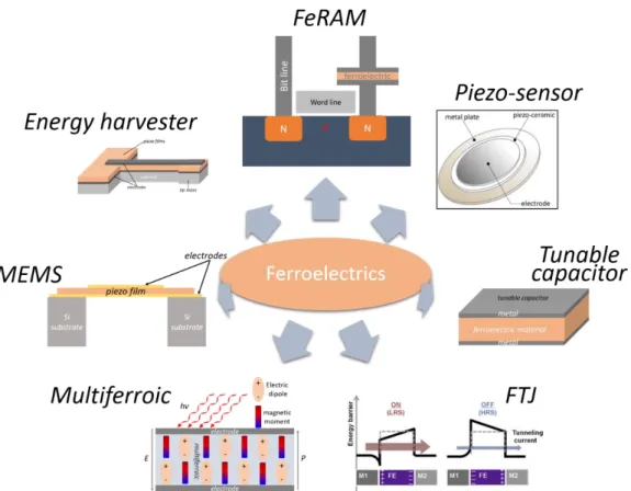
2O)—known as “Rochelle salt” [15]. Ferroelectrics show similar hysteresis behavior as known from ferromagnetics, hence the name. Since then, the research of ferroelectrics has developed for the last 100 years. Nowadays, ferroelectric materials are widely used in various fields ranging from tunable ferroelectric capacitors, piezo-sensors, actuators and microelectromechanical systems (MEMS) [16-19] to ferroelectric random- access memory (FeRAM), multiferroics, ferroelectric tunnel junctions (FTJ), and energy harvesters [20-23], as shown in Fig. 2.1.
Figure 2.1: Various applications of ferroelectrics. Ranging from tunable ferroelectric capacitors, piezo-sensors, and microelectromechanical systems (MEMS) to multiferroics, energy harvesters, ferroelectric tunnel junctions (FTJ) and ferroelectric random-access memory (FeRAM). (Ideas for sketches adapted from ref. [16-23])
5
2.1.1 Dielectricity
Ferroelectric material represents a special type of dielectric material. A key feature of dielectrics is their ability to transmit the electric fields via induction, rather than conduction.
Dielectrics will be electrically polarized if exposed to the electric field. If the applied exterior electric field is not very strong, the polarization P is considered to have a linear relationship with external electric field E:
𝑃 = 𝜀
0𝜒
𝑒𝐸 = 𝜀
0(𝜀
′− 1)𝐸 (2.1) where ε
0is the permittivity of free space, χ
eis the electric susceptibility, ε' is the relative dielectric constant, which is the real component of the dielectric constant 𝜀:
𝜀 = 𝜀
′+ 𝑖𝜀
′′(2.2) where ε'' is the imaginary component of the dielectric constant, indicating the energy loss in the dielectrics. The loss tangent is then defined by:
tan 𝛿 = 𝜀
′′𝜀
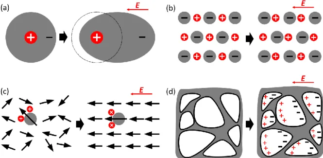
′(2.3) In general, there are four different mechanisms of polarization, i.e. electronic polarization, ionic polarization, polar orientational polarization, and space charge polarization (see Fig.
2.2).
Figure 2.2. Schematics illustrate four types of polarization mechanisms: (a) electronic polarization, (b) ionic polarization, (c) polar orientational polarization, and (d) space charge polarization.
Electronic polarization: The ions (atoms) that form the dielectrics consist of positively charged
nuclei and negatively charged electrons. In the absence of an electric field, the positively and
negatively charged centers coincide. However, in the presence of an exterior electric field,
6
the negatively charged electron cloud will be shifted with respect to the positively charged nucleus, forming an electric dipole and resulting in an electronic polarization (see Fig. 2.2(a)).
The resulting dipole has an electric dipole moment:
𝜇 = 𝑞 ∙ 𝑟 (2.4) where q is the charge and r is the relative displacement vector between the centers of positive and negative charges. In case of linear polarization, the induced dipole moment is proportional to the electric field intensity:
𝜇 = 𝛼
𝑒𝐸
𝑙𝑜𝑐(2.5) where α
eis the electronic polarizability and E
locis the local electric field at the dipole, which can differ from the external electric field E. The electronic polarizability α
eis given by:
𝛼
𝑒= 4𝜋𝜀
0𝑅
3(2.6) where R is the atomic radius. Since R is of order of 10
-10m, α
eis of the order of 10
-40F·m
2. Ionic polarization: In analogy, a relative displacement of positive and negative ions occurs in ionic crystals upon expose to an electric (see Fig. 2.2(b)). The resulting ionic polarizability α
iis given by:
𝛼
𝑖= 12𝜋𝜀
0𝑎
3𝐴(𝑛 − 1) (2.7) where a is the unit cell constant, A is the Madelung constant, n is the electronic repulsion index (in case of ionic crystal, n = 7 to 11). The ionic polarizability has a comparable order with electronic polarizability.
Orientational polarization: Polar dielectrics, e.g. water, are composed of polar molecules.
Polar molecules possess permanent electric dipole moments μ
0due to the net separation of positive and negative charges. Because of thermal motion, these dipoles are disorderly aligned, resulting in a zero macroscopic polarization. However, in the presence of E, the dipoles will be orientated. Since the dipoles have the lowest potential energy when aligned along the direction of electric field, they tend to align along the electric field direction. As a result, a macroscopic polarization is yielded and a polar orientational polarization occurs (see Fig. 2.2(c)). The polar orientational polarizability α
dis given by:
𝛼
𝑑= 𝜇
023𝑘𝑇 (2.8) where k is the Boltzmann constant. Normally, the polar orientational polarizability is much larger than the electronic polarizability (it is of the order of 10
-38F·m
2).
Space charge polarization: the space charge polarization is attributed to the existence of inhomogeneity and interfaces, e.g. grain boundary and phase boundary, in the dielectrics.
Under an applied electric field, the chaotically distributed free charges will move and
7
accumulate at these defective spaces, leading to the space charge polarization (see Fig.
2.2(d)).
The different types of polarization can be distinguished by their frequency dependence.
Generally, the formation of the electronic and ionic polarization takes only 10
-16- 10
-14s and 10
-13- 10
-12s, respectively. Consequently, under an applied ac field, the electronic polarization is able to occur even in the optical frequency regime, while the ionic polarization exists only for frequency lower than 10
13Hz (corresponding to infrared frequency). In comparison, the formation of polar orientational and space charge polarization takes even longer times—10
-10
- 10
-2s and 10
0- 10
3s, respectively. As a result, they only contribute in a relatively low frequency regime. The relationship between dielectric polarization mechanism and frequency is schematically shown in Fig. 2.3.
Figure 2.3. Frequency dependence of dielectric polarization mechanisms.
8
2.1.2 Ferroelectricity
Besides the above-mentioned four polarization mechanisms, ferroelectrics are characterized by a spontaneous polarization P
swhich is present in the ferroelectric temperature range and can be switched by a sufficient large external field. The spontaneous polarization is caused by the nonsymmetry of the crystalline structure. Among the 32 crystallographic point groups, 11 are centrosymmetric and 21 are non-centrosymmetric. Except for 432 cubic class, 20 of these 21 non-centrosymmetric classes exhibit piezoelectricity. 10 of these 20 piezoelectric classes possess spontaneous polarization and exhibit pyroelectricity. If the spontaneous polarization is reversible under electric field, the material is ferroelectric. The structural division of dielectric, piezoelectric, pyroelectric, and ferroelectric crystals is sketched in Fig. 2.4.
Figure 2.4. Relationship between crystallographic symmetry and piezoelectric, pyroelectric and ferroelectric.
The mechanism of spontaneous polarization varies for the different types of ferroelectrics.
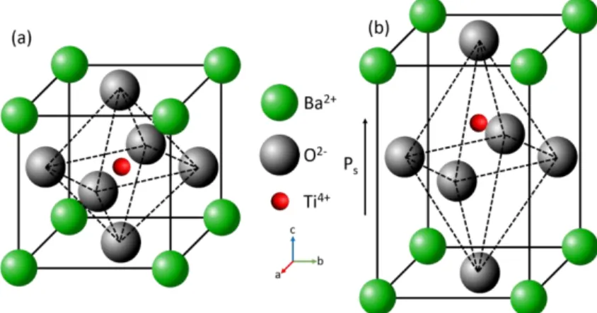
Here we take the displacive type ferroelectric BaTiO
3as an example to explain the origin of spontaneous polarization. The ferroelectricity of BaTiO
3was discovered in 1940s [24], and has attracted great interest for academic research and industrial applications due to its simple structure and excellent electronic properties. BaTiO
3is a typical ABO
3perovskite, where A- and B-site are Ba
2+and Ti
4+, respectively. Ti
4+is surrounded by 6 adjacent oxygens, forming a TiO
6octahedron (see Fig. 2.5). The spontaneous polarization of BaTiO
3exists at temperature below 393 K and disappears above Curie temperature T
C= 393K. At T > T
C, the BaTiO
3has a cubic unit cell (see Fig. 2.5(a)) since the thermal vibrational energy of Ti
4+is too large to allow a stable off-centered position. As a result, the TiO
6octahedron forms a symmetry center and 6 Ti-O electric dipole moments are equal and opposite, canceling each other (P
s= 0). At temperature below T
C, the effect of the electric interaction between Ti
4+and O
2-is stronger than the thermal perturbation, resulting in the deviation of Ti
4+from the symmetry center.
Therefore, the crystal structure is transformed to the tetragonal state (Fig. 2.5(b)), generating
a permanent electric dipole moment along the [001] direction (i.e. spontaneous polarization).
9
Figure 2.5. Structure of a BaTiO3 crystal in the (a) cubic state above the Curie temperature and (b) tetragonal state below the Curie temperature.
The unit cells in a certain small area typically have the same direction of P
sand, thus, form a ferroelectric domain. Domains are separated by domain walls. The P-E hysteresis loop represents a macroscopic description of the domain motion. Fig. 2.6 shows a P-E loop for domains with opposite directions of spontaneous polarization.
Figure 2.6. Typical P-E hysteresis loop of ferroelectrics, assuming the domains possess two opposite directions of spontaneous polarization (up and down). In the absence of E, the initial macroscopic polarization P is zero (point O). In the presence of E, domains coinciding with the direction of E extend, while those with opposite direction shrink (segment OA). The polarization increases with E, and will saturate when all the domains align along the direction of E (point B). Then P increases linearly as E (segment BC). When E is gradually decreased to 0, most of the polarization persists, resulting in a remnant polarization Pr. The remnant polarization will disappear when E reaches -Ec, which is termed as coercive electric field. A further decrease of E inverts the polarization.
10
The ferroelectric domains tend to align along the direction of E. The motion of the domains is actually realized via the formation and development of new domains as well as the motion of domain walls. Before applying an electric field, the macroscopic polarization of the crystal,
𝑃 = ∑ 𝝁
𝑉 (2.9) where μ is the dipole moment and V is the volume, is zero (initial state point O in Fig. 2.6).
When E is applied, domains coincide with the direction of E extend and those with opposite direction shrink. As a result, the polarization P increases with E, corresponding to section OA in Fig. 2.6. As E continues to increase, all the domains will align along the direction of E, leading to a saturated P (point B in Fig. 2.6). If E is further increased, P will increase linearly as E increases, just like the common dielectrics (see segment BC in Fig. 2.6). The extrapolation of BC to E = 0 defines the spontaneous polarization P
s. When E decreases gradually to 0, most of the domains still stay at the polarization direction, resulting in a remnant polarization P
r. The polarization disappears at coercive field -E
c. Further decrease E and P will saturate again.
When E starts to increase, a similar remnant and coercive P-E behavior will be observed, forming a hysteresis loop.
2.1.3 Ferroelectric phase transition
Ferroelectrics undergo a phase transition from T > T
Cdielectric to T < T
Cferroelectric phase.
In many cases, further transitions from one to another ferroelectric can follow. Generally, upon cooling, the lattice symmetry decreases. A typical phase transition sequence is the one from cubictotetragonal toorthorhombicto finallyrohombohedral, as shown in
Fig. 4.2(a) [25].
Figure 2.7. (a) Schematic illustration of the structural distortions of the perovskite BaTiO3 from cubic (T > TC) to tetragonal, orthorhombic, and finally rhombohedral structures below TC. (Reproduced from ref. [25]) (b) Temperature dependence of the permittivity of a signal-domain BaTiO3 crystal (Reproduced from ref. [26]).
11
Fig. 2.7(b) illustrates the phase transitions of a signal-domain BaTiO
3[26]. At temperatures above T
C= 120 °C, BaTiO
3has a cubic structure without spontaneous polarization. When cooled below T
C, BaTiO
3undergoes a para-to-ferro phase transition, which is resulted from a lattice distortion from the cubic to a tetragonal structure. As a result, a spontaneous polarization along the axes of the <001>
pcfamily is generated, where the subscript “pc”
represents “pseudo-cubic”. Upon cooling, a ferro-to-ferro phase transition occurs at T
O-T≈ 0
°C. This structure conversion from tetragonal to orthorhombic switches the direction of P
sto the <110>
pcfamily. Eventually, a second ferro-to-ferro phase transition appears at around - 90 °C, leading to a lattice distortion from the orthorhombic to a rhombohedral structure.
Consequently, the direction of P
sis switched to the <111>
pcfamily.
During the ferroelectric phase transitions, the properties of ferroelectrics change strongly, the T-dependence of the permittivity typically shows characteristic sharp peaks at the phase transition temperatures (Fig. 2.7(b)).
2.1.4 Piezoelectricity
In 1880, piezoelectric effect was discovered by Pierre Curie and Jacques Curie in quartz crystals. When a mechanical stress is applied on a piezoelectric crystal, opposite charges of identical amount will be generated on both sides of the crystal, i.e. piezoelectric effect. In opposite, if an external electric field is applied on a piezoelectric crystal, a mechanical strain will be generated. This is termed as the converse piezoelectric effect. Piezoelectric and converse piezoelectric effects are equivalent, i.e. materials exhibiting the piezoelectric effect also possess the converse piezoelectric effect. They can be described by:
𝐷
𝑖= 𝑑
𝑖𝑗𝑘𝜎
𝑗𝑘, 𝑎𝑛𝑑 (2.10) 𝑆
𝑖𝑗= 𝑑
𝑖𝑗𝑘𝐸
𝑘(2.11) respectively, where D
iis the dielectric displacement vector, 𝜎
jkis the stress tensor, S
ijis the strain, d
ijkis the piezoelectric coefficient, and the subscriptions i, j, and k represent three axes.
Figure 2.8. Schematic illustration of the origin of piezoelectricity in a quartz crystal showing a piezoelectric material (a) without application of mechanical stress, (b) with a x-axis compressive stress and (c) with a y-axis compressive stress.
12
It has been shown in chapter 2.1.2 that among the 32 crystallographic point groups, only 20 non-centrosymmetric classes exhibit piezoelectricity. Here quartz crystal is taken as an example to interpret the origin of piezoelectricity in crystals. The chemical formula of quartz is SiO
2, and has no center of symmetry. For the convenience of interpretation, Si and O atoms are numbered in Fig. 2.8. Without application of stress, the positive and negative charges centers coincide, i.e. no surface charge accumulation (see Fig. 2.8(a)). When a compressive strain is applied along the x axis, Si atom 1 is squeezed in between O atoms 2 and 6, while O atom 4 is squeezed in between Si atoms 3 and 5. Consequently, surface A is negatively charged, while surface B becomes positively charged (see Fig. 2.8(b)). This type of piezoelectric effect is called longitudinal piezoelectric effect. In case of a y-axis stress, O atoms 2 and 6, as well as Si atoms 3 and 5 will move simultaneously with the same displacement, therefore, no charge will appear on left and right surface. However, Si atom 1 and O atom 4 will be pushed outwards, resulting in a positively charged surface A and negatively charged surface B (see Fig. 2.8(c)). In contrast to the longitudinal piezoelectric effect, this type of piezoelectric effect is called transverse piezoelectric effect. When the quartz crystal is stretched or compressed along the z axis, no bound charges will appear at the surface.
2.2 Engineering of ferroelectricity
Typically the best ferroelectric properties, e.g. large permittivity, piezoelectricity and tunability, can be achieved at the para-to-ferro or ferro-to-ferro phase transition temperature. Unfortunately, these temperatures generally deviate from room temperature (RT) [26-29], which represents the operation T of most electronics. The most commonly used methods to modify the phase transition temperature of ferroelectrics are doping of the material with adequate elements, mechanical strain or the transformation to a so-called relaxor-type ferroelectric.
2.2.1 Doping
Doping with higher-charged or lower-charged cations can tune the lattice structure via distortion, tilting, or rotation, which automatically leads to a modification of the ferroelectric properties [30-34].
In the K
xNa
1-xNbO
3system which is the system used for this work, Li, Ta, Sb, and Mn are the most commonly used elements to shift the phase transition temperature [35]. A doping with Li will lead to an increase of T
Cwith a rate of 8 to 12 °C / mol% and a decrease of T
O-Twith a rate of 22 to 35 °C / mol% [36-39]. Elements like Sb and Ta are often used to substitute the B- site of ABO
3-type perovskites. A doping of Sb will result in a decrease of 22 °C / mol% to T
Cand 12 °C / mol% to T
O-Tin (K
0.48Na
0.52)(Nb
1-xSb
x)O
3ceramics [40]. It should be noted that Sb is toxic, which limits its application. The doping with Ta decreases T
Cand T
O-Twith a rate of 5 to 7 °C / mol% and 3 to 5 °C / mol%, respectively, in (K,Na)(Nb
1-xTa
x)O
3systems [41-43].
Furthermore, MnO
2can also markedly decrease T
O-Tin K
xNa
1-xNbO
3system [44].
13
Figure 2.9. Doping effects on the phase transition temperatures of KxNa1-xNbO3 ceramics (reproduced from ref.
[29]).
The impact of different substitutions on the phase transition temperature of K
xNa
1-xNbO
3ceramics is summarized in Fig. 2.9. Note that various co-doping strategies, e.g. Li-, Ta- and Sb-
co-doping, have been investigated recently to further tune the phase transition temperature
of K
xNa
1-xNbO
3ceramics and therefore their piezoelectric and ferroelectric properties.
14
2.2.2 Strain
In case of epitaxial strain, the lattice misfit β and the misfit-induced in-plane biaxial strain ϵ
sare defined by:
𝛽 = 𝑎
0− 𝑎
𝑠𝑢𝑏𝑎
𝑠𝑢𝑏(2.12) 𝜖
𝑠= 𝑎 − 𝑎
0𝑎
0(2.13) where a
0and a are the lattice parameters of unstrained and strained films, respectively. And a
subis the substrate lattice parameter. A positive ϵ
sindicates a tensile in-plane strain, whereas a negative ϵ
sindicates a compressive in-plane strain (see Fig. 2.10). Due to the Poisson effect, the in-plain strain will be compensated by an opposite out-of-plane strain.
Fig. 2.10. (a) tensile and (b) compressive in-plane strain in epitaxial films. The in-plane strain is compensated by an opposite out-of-plane strain due to the Poisson effect.
The lattice misfit-induced strain will (i) either introduce defects (vacancies, dislocations, or cracks) or (ii) distort the lattice structure so that the electronic properties of ferroelectric will be modified. Pertsev et al [12,13] first proposed that the epitaxial strain can induce the shift of T
Cfor epitaxially grown SrTiO
3thin films.
Based on a thermodynamic analysis and single-domain assumption, Pertsev et al [13,45]
proposed that the shift of T
Cfor a SrTiO
3thin film under a tensile strain is given by:
∆𝑇
𝐶= 2𝜀
0𝐶 𝑄
11+ 𝑄
12𝑠
11+ 𝑠
12𝜖 (2.14)
where C is the Curie-Weiss constant, Q
ijthe electrostrictive coefficients and and s
ijthe elastic
compliances.
15
Figure 2.11. Theoretical calculation of the shift of TC along the enhanced polarization direction (see arrows in the insets) for SrTiO3. The region marked by black dashed lines represents the expected range of the phase transition temperature, depending on the material constants obtained from the literatures. (Adapted from ref. [45])
The theoretical prediction ofT
Cin SrTiO
3system is shown in Fig. 2.11. The T
Calong the tensile-strain direction is always enhanced. The broad distribution of T
C(dashed area) is due to the various reported material parameters. The theoretical expectation has been verified by the experimental researches [46].
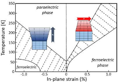
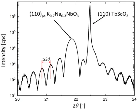
Figure 2.12. T-dependence of permittivity of unstrained bulk NaNbO3 (black line) and compressively strained NaNbO3 film (red line). The phase transition of polycrystalline NaNbO3 from R-phase antiferroelectric state to P- phase antiferroelectric state at ~ 620 – 660 K is shifted to ~ 125 K. (Adapted from ref. [50])
Cai et al [47-50] later demonstrated a decrease of T
Cin compressively strained NaNbO
3thin
films (see Fig. 2.12). Their work provided the possibility of tuning the phase transition to a
lower temperature via epitaxial strain.
16
2.2.3 Relaxor
Relaxors were first discovered in the BaTiO
3-BaSnO
3system in 1954 [51]. The phase transitions of relaxors possess the features of frequency dispersion and electric field dependence, making it convenient to tune their ferroelectricity. Therefore, the introduction of the relaxor is also widely used for the engineering of ferroelectricity.
Table 2.1. Comparison of relaxor-type ferroelectrics and conventional ferroelectrics. (Adapted from ref. [50])
Item Conventional ferroelectric Relaxor-type ferroelectric
P-E hysteresis loop
Typical P-E loop
Strong P
r Slim P-E loop
Weak P
rT-dependence of P
P decays dramatically with T
P drops down to zero above T
C P decreases smoothly with T
Non-zero P above T
maxPhase transition
Structural phase transition
Sharp and narrow peak
No frequency dispersion
Curie-Weiss law for T > T
C Transition of PNR mobility
Broad peak
Frequency dispersive
Curie-Weiss law for T > T
Burns17
Typically, relaxor properties can be introduced to epitaxial thin films, especially under the presence of plastic strain relaxation [52]. The compositional inhomogeneity in nano-scale contributes to the formation of so-called polar nanoregions (PNR), which are micro- or nano- regions with uniform dipolars. The relaxor ferroelectrics exhibit paraelectric properties at high temperature with the absence of PNRs, which is similar to the paraelectric properties of conventional ferroelectrics. Upon cooling, the relaxors will be turned into an ergodic relaxor state with the presence of randomly distributed PNRs. The PNRs can be re-orientated under E-field, which makes it possible to tailor the ferroelectric and surface acoustic wave properties of the relaxors (see chapter 6).
For better understanding, the main differences between relaxor and conventional ferroelectrics are summarized in table 2.1.
Generally, the differences between relaxors and conventional ferroelectrics are concentrated on three aspects:
(i) P-E hysteresis loop. The PNRs of relaxors tend to distribute randomly with the absence of electric field due to their thermal motion. Consequently, relaxors show a slim P-E hysteresis loop with a weak remnant polarization P
rat zero electric field. In case of conventional ferroelectrics, the spontaneous polarization persists at E = 0, therefore it shows a strong P
rand a typical P-E loop.
(ii) T-dependence of polarization. Since the PNRs persist above the temperature of maximum permittivity T
max, relaxors show a non-zero polarization above T
max. In contrast, the polarization in conventional ferroelectrics drops dramatically with temperature and reaches zero at T
C, indicating the disappearance of spontaneous polarization above T
C.
(iii) Phase transition. Unlike the structural phase transition of conventional ferroelectrics, the phase transition of relaxors implies a decrease of the mobility of PNRs.
Consequently, the relaxors normally show a broad and frequency dispersive phase transition in the vicinity of T
max. T
maxincreases with frequency. Moreover, the Curie- weiss law doesn’t apply at T < T
Burns. In contrast, the conventional ferroelectrics show a sharp and narrow phase transition with no frequency dispersion. The permittivity- versus-temperature relation follows nicely the Curie-Weiss law at T > T
C.
Researchers proposed a series of models to describe the relaxor behavior. Smolenskii et al [53] proposed an inhomogeneous micro-region model which is well accepted to explain the broad transition at the Curie temperature. Cross [54] further improved the model by analogizing local polar micro-regions to spin cluster in superparamagnets, i.e. he developed a
“superparaelectric model”. Recently, models like dipole glass model [55,56], breathing mode
model [57], and random-field model [58,59] are proposed to explain the relaxor state at low
18
temperature. The difference of these models is essentially focused on the question whether the relaxor state at low temperature is
(i) a glass state with randomly distributed PNRs that similar to dipolar glasses or
(ii) a ferroelectric state with the domains broke up into nano scale due to the quenched random electric fields.
Figure 2.13. Comparison of dipolar glass model and random-field model that describe the evolution of PNRs in an epitaxially strained (K,Na)NbO3 film. The insets show the different relaxor states at different temperatures.
(Adapted from ref. [50])
The evolution of PNRs in an epitaxially strained (K,Na)NbO
3film is described by two different
models in Fig. 2.13. At temperatures T
max< T < T
Burns, PNRs are randomly distributed in the
matrix. As temperature decreases, the dipolar glass model indicates that a dipolar glass state
is formed below the static freezing temperature T
VF≈ 200 K, below which PNRs become
immobile. In contrast, the random-field model suggests that at T
VFa ferroelectric ordered
domain breaks up into nano scale domains which is attributed to the quenched random
electric fields.
19
2.3 Surface acoustic waves
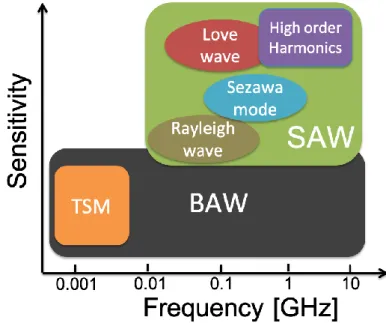
Surface acoustic waves (SAW) were first investigated by Lord Rayleigh in 1885 [60]. SAWs represent acoustic waves propagating along the surface (or interface) of materials. The amplitude of a SAW has the maximum value A at the surface, and it attenuates exponentially with depth into the material. The penetration depth d of the SAW, which is defined by the attenuation of the amplitude to a value A/e, depends on wavelength λ which is typically in the μm range. Therefore, most of the acoustic energy is concentrated near the surface, making the SAW sensitive to surface perturbations like mechanical deformation, physical absorption, or chemical reaction, and thus facilitating sensors applications. Moreover, when coupled with a fluid, the acoustically induced force or pressure can cause steady acoustic streaming that can efficiently drive the liquid or manipulate the particles, enabling a broad range of actuator applications such as liquid mixing, jetting, nebulization, particle manipulation, patterning or sorting [61]. The major applications of SAWs are shown in Fig. 2.14.
Figure 2.14. Major applications of surface acoustic waves, including liquid mixing and atomization, particle manipulation, patterning, and sorting as well as sensing. (Ideas for sketches adapted from ref. [61])
2.3.1 Surface acoustic wave modes
Based on the different vibration modes and generation systems (layered or bulk), surface
acoustic waves generally can be classified as Rayleigh mode SAW, shear horizontal mode SAW
(SH-SAW), Love mode SAW, and Sezawa mode SAW [62]. Fig. 2.15 shows the major modes of
SAWs and their vibration schematics.
20
In the Rayleigh mode, particles on the surface vibrate elliptically, i.e. the Rayleigh wave possesses two vibration components, one normal to the surface, the other parallel to the propagation direction (see Fig. 2.15(a)). The amplitude of Rayleigh waves, which is normally sub-nano meter to a couple of nanometers, decays exponentially with the depth into the substrate. In general, Rayleigh waves can only penetrate one wavelength deep into the propagation media. As a result, most energy of the Rayleigh wave is confined at the surface, which makes it very sensitive to surface perturbations, providing an advantage over bulk acoustic wave (BAW) in case of sensor applications. The Rayleigh waves can operate at fundamental mode or higher orders of harmonics. Especially in thin film systems, the high orders of harmonics can be generated to further improve the operation frequency of the SAWs, which will be discussed in Chapter 5.
Figure 2.15. Major modes of surface acoustic waves: (a) Rayleigh mode SAW (b) Sezawa mode SAW (c) Love mode SAW and (d) shear-horizontal mode SAW (SH-SAW). (Ideas of sketches adapted from ref. [62-67])
Sezawa waves represent high modes of Rayleigh waves, which are typically generated in
“slow-on-fast” layered systems. This means that, in order to generate a Sezawa wave, the acoustic wave velocity in the piezoelectric top layer (for instance a film) should be smaller than that in the non-piezoelectric bottom layer (for instance a substrate) (see Fig. 2.15(b)).
Normally the Sezawa wave propagates faster than the corresponding Rayleigh wave, yielding a higher operation frequency, which offers an advantage over fundamental Rayleigh SAWs when applied as a sensor. The effective thickness of the layered system t
e= hk, where h is the film thickness and k = 2 / is the wave vector, determines the generation of Sezawa waves.
In general, if hk << 1, the generation of Sezawa waves becomes very difficult, instead, the high
orders of Rayleigh waves are generated in the film [63-65].
21
In the Shear horizontal (SH) mode, particles on the surface vibrate in-plane and perpendicularly to propagation direction (see Fig. 2.15(d)). Since there is no out-of-plane vibration component, SH-SAWs hardly dissipate any energy into a liquid on the surface, which giving this mode an advantage over Rayleigh mode SAWs in liquid sensing applications [66].
For actuation applications, the displacement component normal to the surface is required.
Finally, Love waves are typically generated in layered systems. Generally, in order to generate Love waves, a top layer with a much lower acoustic velocity is deposited on the SH-SAW device as a wave guide (see Fig. 2.15(c)). Consequently, the acoustic energy is mostly trapped in the guiding layer, providing high energy density and thus a high sensitivity. Due to their high sensitivity and the absence of surface-normal displacement components, Love waves are widely used in liquid sensing applications [67].
Generally, compared to BAWs, SAWs have the advantages of a high sensitivity, a possible miniaturization, compactness and integration, and a low-energy cost. These are the reasons why SAWs have attracted extensive interest in academy and industry.
2.3.2 Generation and detection of surface acoustic waves
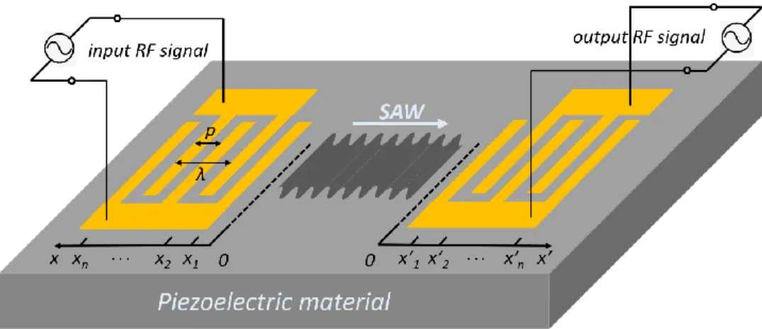
Based on R. M. White and F. W. Voltmer’s work in 1965 [68], SAWs can directly be generated and detected by spatially periodic electrodes, i.e. interdigital transducers (IDT), which can be positioned directly on the surface of a piezoelectric material (see Fig. 2.16).
Figure 2.16. Schematic of SAW generation and detection with IDTs on a piezoelectric material.
Input and output IDTs can be used as generator and receiver of SAWs. A periodic electric field
is produced when an ac voltage is applied to the input transducer, resulting in a periodic strain
field due to the inverse piezoelectric effect. As a consequence, a traveling SAW is generated
that propagates bidirectionally with sub-nanometer surface displacement normal or/and
parallel to the surface.
22
The strongest response of the transducer can be achieved if the SAW wavelength is equal to the interdigital period 2p, where p is the electrode pitch, see Fig. 2.16. It corresponds to the fundamental mode of the SAW at the center frequency:
𝑓
0= 𝑣
2𝑝 (2.15) where v is the SAW phase velocity in the piezoelectric media. Table 2.2 gives typical phase velocities of SAWs in commonly used piezoelectric materials [69-73].
Table 2.2: Properties, including parameters of the SAW velocity v, the temperature coefficient of frequency (TCF), the electromechanical coupling coefficient K2, and the permittivity ε', of commonly used piezoelectric materials for SAW applications.
Material v (m/s) TCF (ppm/K) K
2(%) ε'
YZ LiNbO
3[69] 3488 -94 4.5 46
128°YX LiNbO
3[69] 3979 -75.4 5.4 55
XY20°LiNbO
3[69] 3727 -65 1.6 74
XY120°LiNbO
3[69] 3403 -75.7 4.1 52
ST-X Quartz [70] 3159.3 0 0.11 3.7
Y-Z LiTaO
3[70] 3230 35 0.74 -
X-112°Y LiTaO
3[70] 3301 18 0.64 52
La
3Ga
5SiO
14[71] 2765 7 0.51 -
(001)-<110> GaAs [70] 2864 35 0.07 12.9
ZnO [70] 2645 15 1.8 10
(0001) AlN [70] 5607 19 0.30 8.5
PZT:Nb [72] 2102 - 54 1242
(Na
0.5K
0.5)NbO
3-SrTiO
3[73] 3120 -345 36.1 888
A delta-function model has been proposed by D. Morgan et al to evaluate the transducer
response [74]. In this model, every electrode is regarded as a wave source and electrodes
reflections are considered to be negligible. Under these assumptions, each electrode can
launch a SAW with phase velocity v and wavenumber k = ω/v, where ω = 2πf. In a linear
23
system, the SAW at any position can be termed as a superposition of SAWs generated by each electrode. The following discussion partially follows the discussion in ref. [74].
The electrical potential φ
sassociated with the wave generated by the n
thelectrode is:
𝜙
𝑠𝑛(𝑥, 𝜔) = 𝑉𝐸(𝜔)𝑃̂
𝑛𝑒𝑥𝑝[𝑖𝑘(𝑥 − 𝑥
𝑛)] (2.16) where V is the input voltage, 𝑃̂
𝑛is defined as the polarity of electrode n with 𝑃̂
𝑛=1 for the live electrodes and 𝑃̂
𝑛= 0 for the grounded electrodes, 𝐸(𝜔) is an element factor which allows for physical processes. Assuming a linear system, the total wave amplitude can be obtained by summing the contribution of each electrode. Defining 𝜙
𝑠(𝜔) as the summation potential of N fingers at x = 0 (see Fig. 2.16) we obtain:
𝜙
𝑠(𝜔) = ∑
𝑁𝑛=1𝜙
𝑠𝑛(0, 𝜔) = 𝑉𝐸(𝜔) ∑
𝑁𝑛=1𝑃̂
𝑛𝑒𝑥𝑝(−𝑖𝑘𝑥
𝑛) (2.17) For simplicity, an array factor A(ω) is introduced:
𝐴(𝜔) = ∑ 𝑃̂
𝑛𝑁
𝑛=1
𝑒𝑥 𝑝(−𝑖𝑘𝑥
𝑛) (2.18)
Combining eq. 2.17 and eq. 2.18, we obtain 𝜙
𝑠/𝑉 = 𝐸(𝜔)𝐴(𝜔).
In a uniform IDT, as shown in Fig. 2.16, the coordinates of electrode centers are 𝑥
𝑛= 𝑛𝑝, with 𝑃̂
𝑛= 0, 1, 0, 1, … Then A(ω) becomes a sum of 𝑁
𝑝= N/2 terms:
𝐴(𝜔) = ∑ 𝑒𝑥𝑝 (−2𝑖𝑛𝑘𝑝)
𝑁𝑝
𝑛=1
= 𝑠𝑖𝑛 𝑁
𝑝𝑘𝑝
𝑠𝑖𝑛 𝑘𝑝 𝑒𝑥𝑝[−𝑖(𝑁
𝑝+ 1)𝑘𝑝] (2.19) Eq. 2.19 gives a series of maxima at kp = n𝜋, i.e. at f
n= nf
0.
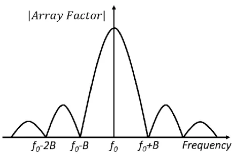
The amplitude difference between fundamental and harmonics is not reflected in A() since the element factor E() effect has to be considered [75,76].
In the fundamental mode, kp . Defining 𝜃 = 𝑘𝑝 − 𝜋 = 𝜋(𝑓 − 𝑓
0)/𝑓
0, then 0 and sin(kp) = sin(-𝜃) -𝜃, and the magnitude of the array factor can be approximated by:
|𝐴(𝜔)| ≈ 𝑁
𝑝| sin (𝑁
𝑝𝜃)
𝑁
𝑝𝜃 | (2.20) Assuming that the element factor E() is constant, then the frequency response of A() represents the frequency response of the transducer, which is shown in Fig. 2.17. The strongest response occurs at the center frequency f
0and attenuates as the operation frequency deviates from the center frequency. The zeros next to the fundamental center frequency f
0occur at:
𝑓 − 𝑓
0= ± 𝑓
0𝑁
𝑝= ±𝐵 (2.21)
24
where B=𝑓
0/𝑁
𝑝is defined as the transducer bandwidth.
Figure 2.17. Frequency response of array factor A(ω) in the region of the fundamental response. The bandwidth B=f0/Np is marked in the figure.
In practice, the SAW system shown in Fig. 2.16 is regarded as a two-port network, the SAW is normally detected by measuring the frequency spectrum of the insertion loss IL(dB)=
10 log
10(𝑃
𝑖𝑛/𝑃
𝑜𝑢𝑡), where 𝑃
𝑖𝑛is the input power, 𝑃
𝑜𝑢𝑡is the power received at the output port. The frequency spectrum of insertion loss shows a characteristic sin(X)/X behavior, as shown in Fig. 2.18. The SAW information such as bandwidth B, center frequency f
0, and phase velocity v can be extracted from the frequency spectrum and will be discussed in chapter 5.
Figure 2.18. Frequency response of insertion loss in a two-port SAW system. The inset shows the layout of a two- port SAW system.