Charging phenomena in single molecules
and ordered molecular islands
DISSERTATION ZUR ERLANGUNG DES DOKTORGRADES DER NATURWISSENSCHAFTEN (DR. RER. NAT.)
DER FAKULT¨AT F ¨UR PHYSIK DER UNIVERSIT¨AT REGENSBURG
vorgelegt von:
Philipp Thomas Scheuerer aus Regensburg
Im Jahr 2020
Pr¨ufungsausschuss:
Vorsitzender: Prof. Dr. J¨org Wunderlich 1. Gutachter: Prof. Dr. Jascha Repp 2. Gutachter: PD Dr. Andrea Donarini Weiterer Pr¨ufer: Prof. Dr. John Lupton
Contents
1 Introduction 1
2 Theoretical background 3
2.1 Scanning Tunneling Microscopy . . . . 3
2.1.1 Scanning Tunneling Spectroscopy . . . . 5
2.1.2 Double barrier tunneling junction . . . . 6
2.2 Atomic Force Microscopy . . . . 7
2.2.1 Kelvin probe force spectroscopy . . . . 9
2.2.2 Dissipation . . . . 11
2.3 Charge transfer processes in SPM . . . . 13
2.4 Alternate-charging scanning tunneling microscopy . . . . 16
2.5 AFM with functionalized tips . . . . 17
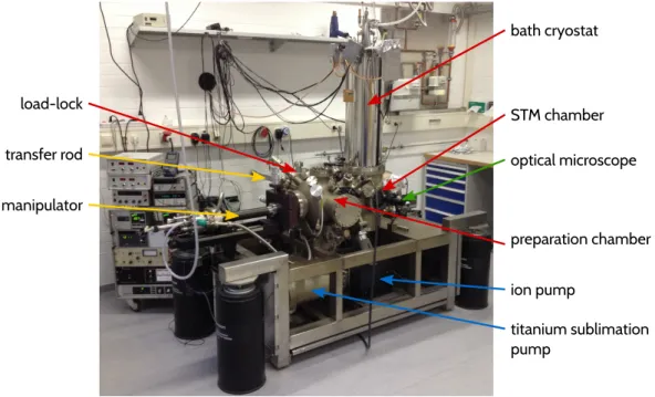
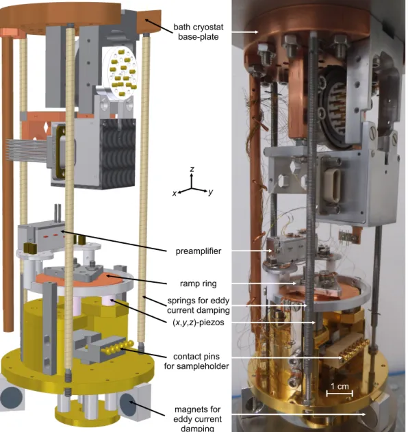
3 Experimental setup and methods 19 3.1 Experimental setup . . . . 19
3.1.1 The scan unit . . . . 19
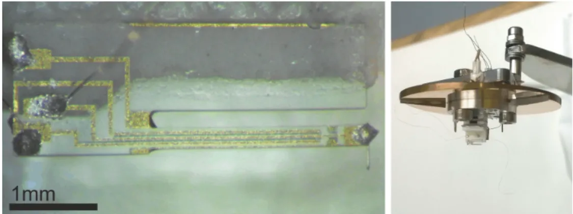
3.1.2 qPlus sensor . . . . 20
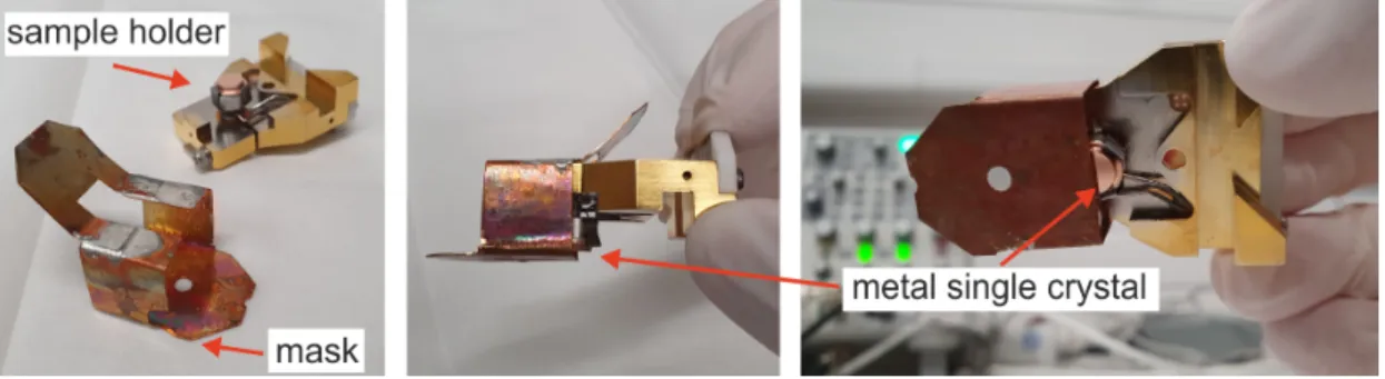
3.2 Sample preparation . . . . 22
4 Determination of structural relaxations in a single molecule upon charging 25 4.1 Introduction . . . . 26
4.2 Methods . . . . 27
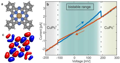
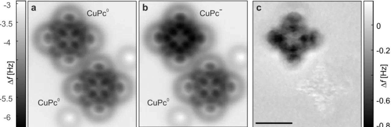
4.3 Charge bistabiltiy of CuPc . . . . 27
4.4 Analysis of the AFM contrast . . . . 28
4.5 Electrostatic contributions to AFM contrast . . . . 32
4.5.1 Disentanglement of geometrical and charge contributions . . . 33
4.5.2 Role of a possible tip polarization . . . . 35
4.6 Structural changes upon charging . . . . 36
4.7 Conclusion . . . . 38
5 Molecular self-assembly on insulating films 39 5.1 Introduction . . . . 39
5.2 Au(110) . . . . 40
5.3 Growth Characterization of NaCl/Au(110) . . . . 41
5.4 Molecular self assembly of PTCDA on NaCl/Au(110) . . . . 43
5.5 NaCl-induced reduction of the sample work function . . . . 45
6 Probing the electron distribution and electron transfer in charged self-
assembled PTCDA islands 47
6.1 Introduction . . . . 48
6.2 Sample preparation and methods . . . . 50
6.3 Geometrical structure of self-assembled PTCDA islands . . . . 50
6.4 Determination of the charge state of PTCDA on NaCl(22ML) . . . . 51
6.5 Controlled charging and charge-state detection of a self-assembled PTCDA island . . . . 53
6.6 Spatial dependence of the charging with one excess electron . . . . . 54
6.7 AFM images at different bias voltages . . . . 58
6.8 Origin of the dissipation signatures . . . . 61
6.9 Possible mechanisms for tip-induced energy level shifts . . . . 62
6.10 Electrostatic model of the energy level alignment . . . . 64
6.11 Simulated spatial dependence of the electron distribution . . . . 67
6.12 Estimation of tunneling rates . . . . 69
6.13 Contrast changes induced by a defect in proximity to the island . . . 70
6.14 Probing the electron distribution in a 2-by-2 and 2-by-4 island . . . . 73
6.15 Conclusion . . . . 77
7 Stabilizing a confined out-of-equilibrium state by polaronic shifts 79 7.1 Introduction . . . . 79
7.2 Sample preparation . . . . 81
7.3 Geometric structure of self-assembled PTCDA islands . . . . 81
7.4 Switching of PTCDA molecules within self-assembled PTCDA islands 82 7.4.1 Switching PTCDA molecules . . . . 82
7.4.2 Switching single PTCDA molecules within an island: STS- measurements . . . . 85
7.4.3 The effect of switching on the local contact potential difference 86 7.4.4 Structural changes upon switching . . . . 88
7.4.5 Further observations . . . . 91
7.5 Switching of individual PTCDA molecules . . . . 92
7.5.1 Determination of the charge state . . . . 92
7.5.2 Changes in the electronic structure of PTCDA upon switching 95 7.5.3 Structural changes of individual PTCDA upon switching . . . 97
7.6 Proposed mechanism for the switching of PTCDA . . . . 99
7.7 Conclusion . . . 103
8 Summary 105
Bibliography 109
Abbreviations 129
Acknowledgement 131
1 Introduction
Electron transfer is ubiquitous in nature and plays a central role, for example, in chemical reactions such as photosynthesis or corrosion, as well as organic light- emitting diodes, transistors, and photovoltaic devices.
Even though electron transfer processes are generally well understood, their investi- gation at the atomic-scale could provide novel insights and push forward the ongoing development of organic electronics.
Scanning tunneling microscopy (STM) and atomic force microscopy (AFM) have made tremendous progress since their invention in the 1980s [1, 2]. Especially within the past 20 years, those techniques have become powerful tools for atomic-scale surface characterization, and in particular, for the investigation of single atoms or molecules and their properties in real space.
Already shortly after its invention, STM was used to controllably move single Xe atoms on a metallic surface [3]. Another impressive example was the measurement of vibrational and rotational excitations of single molecules, adsorbed on a surface [4, 5].
After it was found that ultra-thin insulating films can be used to decouple a molecule from the supporting conductive substrate [6], scanning tunneling microscopy has been exploited for electronic structure investigations of single molecules, for example, to map the frontier orbitals of an individual molecule [6]. One of the most relevant applications of STM for this thesis is the possibility to resolve and manipulate charge states of single atoms and molecules [7, 8]. This possibility of charge state control was utilized to derive the distribution of an excess electron within a molecule, based on the electron’s impact on the tunneling barrier [8].
Also, AFM has provided fascinating insights into physical and chemical processes at the atomic scale. Whereas STM primarily measures the electronic properties of single molecules, the strength of atomic force microscopy is its sensitivity to the geomet- ric structure of single molecules, which makes those two techniques complementary.
The discovery that AFM with CO-functionalized tips enables to resolve the details of the chemical structure within single molecules represents another recent break- through [9]. This technique was proven to be even sensitive enough to distinguish bond order differences within single molecules [10].
Furthermore, it was shown that charge states of single molecules can be resolved and manipulated by means of AFM [11]. Recently, it was demonstrated how bond orders within a molecule change upon charging by combining the ability of charge manipulation and structural resolution [12].
Those examples show that STM and AFM, in combination, provide us with a com-
plete toolbox for the investigation of electron transfer processes within single mole- cules.
In this thesis, we make use of STM and AFM to study and resolve the structural and electronic effects accompanying electron transfer reactions within single molecules and small ordered islands of molecules with atomic-scale resolution. The experiments, which will be presented in this thesis, can be divided into three projects:
The effect of charging on the geometric structure of a single molecule.
In chapter 4, AFM experiments of individual molecules adsorbed on ultrathin NaCl films, which were grown on a supporting metal surface, are presented. Individual molecules were controllably switched between two different charge states using scan- ning probe microscopy. We acquired AFM images of single molecules in both charge states and analyzed the differences in image contrast. From those contrast changes in AFM images due to charging and supporting density functional theory (DFT) simulations, the geometrical changes of a molecule upon charging were elucidated.
The stability of electron distributions within molecular islands in different charge states, and the role of electrostatic interactions.
Chapter 6 is the main project of this thesis. For these experiments, we grew highly- ordered islands, consisting of a few tunnel-coupled molecules, by a thermally activated diffusion process known as molecular self-assembly [13]. The islands were grown on a many monolayers thick NaCl film on a supporting Au(110) substrate, to suppress charge transfer between molecular islands and the metal substrate. We probe and manipulate the charge state of self-assembled molecular islands with single-electron control by means of AFM [14, 15]. From imaging and spectroscopy, we could gain insight into the distribution of excess electrons within an island. We found that the islands exhibit a probe-driven intra-island electron transfer in most charge states.
This allows us to directly observe and simulate the mutual interactions between in- dividual charges and the stability of specific charge configurations within atomically- precise ordered molecular structures.
We find that the total number of excess electrons within a molecular island has a cru- cial influence on the stability of their distribution. Finally, we estimate the tunneling rates of the intra-island charge transfer from the experimental data.
A novel tentative mechanism of charge stabilization in a single molecule, based on strong polaronic shifts due to charge confinement.
In chapter 7, experiments on self-assembled PTCDA islands and individual PTCDA molecules on ultrathin NaCl films are presented. It was found that PTCDA mole- cules can be switched by applying voltage pulses. STM and AFM images suggest that this switching is related to charging, accompanied by structural changes. How- ever, instead of occupying the lowest unoccupied molecular orbital, the experiments suggest that the excess charge could be localized at a molecule’s functional group.
There, it might be stabilized due to an exceptionally large energy gain, arising from strong spatial confinement of the excess electron.
2 Theoretical background
In this chapter, the imaging techniques and the underlying principles of scanning tunneling microscopy (STM) and atomic force microscopy (AFM) are introduced, which are commonly summarized under the term scanning probe microscopy (SPM).
Further, a brief overview of specific imaging techniques will be given that were used in the experiments.
2.1 Scanning Tunneling Microscopy
In 1981 Binnig et al. reported on an experimental setup that enabled tunneling through a vacuum gap with precise control of the tunnel barrier width [16]. Shortly afterwards, they presented the first scanning tunneling microscope, which allowed to resolve conductive surfaces with atomic-scale resolution [1, 17].
Figure 2.1a shows the basic setup of an STM. It consists of an atomically sharp metal tip, whose position can be controlled with sub-angstrom accuracy in x-,y- and z-direction, and a flat conductive sample to be probed. If the tip is positioned sufficiently close (a few angstroms) to the sample surface and a bias voltage is applied, there is a finite probability for electron tunneling between tip and sample through the vacuum barrier, which gives rise to a measurable tunneling current. By recording this tunneling current while raster-scanning the sample, atomic-scale surface profiles can be obtained. This can be done in two different operational modes: in constant- height modethe tip is raster-scanned at a pre-defined plane above the sample surface.
The obtained image contrast is then based on variations in the measured tunneling current.
Alternatively, as depicted, in constant-current mode the vertical position of the tip is adjusted by a feedback loop to keep the tunneling current at a predefined value.
The working principle of STM is based on the effect of quantum mechanical tunneling.
In a one-dimensional picture of tunneling through a potential barrier, tip and sample can be considered as two metal electrodes separated by a potential barrier of height Φ and width 2a, corresponding to the vacuum gap between tip and sample (see Fig.2.1b). For simplicity, it is assumed that the work functions Φ of tip and sample are identical. By applying a positive bias voltage to the sample with respect to the tip, the Fermi levels are shifted with respect to each other, such that in the sample unoccupied states become available for electrons below the Fermi level in the tip.
In the following consideration it is assumed that the potential Φ is constant within
−a < z < a (the latter is valid in the limit of small bias voltages V << Φ/e). In a classical picture, an electron of energy E < Φ, propagating in +z-direction, would simply be reflected at the barrier. In quantum mechanics, an electron is described by a wave function ψ(r, t), and its probability density is given by |ψ(r, t)|2[18].
tip vac sample
z a
-a b
a
x,y
tip
sample voltage V
I z
sample
tip height
Re(Ψ)
F
EF,S
EF,T
F Evac
I e|V|
0
z x,y
Figure 2.1: a The operation principle of an STM, using constant-current mode.
b Schematic picture of quantum mechanical tunneling through a one- dimensional potential barrier. Tip and sample resemble the two elec- trodes separated by a potential barrier of height Φ. Further, the real part of an electron wave function of energyE < Φ is depicted, for prop- agation in +z-direction. after [19, 20]
To obtain the transmission probability for an electron of energyE through the barrier, the stationary Schr¨odinger equation has to be solved separately for the tip, sample, and vacuum region [18]. Outside the vacuum gap, where the electron can freely propagate, the solution is given by
ψ(z) =Aeikz+Be−ikz for z <−a (2.1)
ψ(z) =F eikz +Ge−ikz for a < z (2.2) with a wave number k=√
2mE/¯h. Within the vacuum gap the solution reads as ψ(z) = Ce−κz+Deκx for −a < z < a (2.3) with a wave numberκ=p
2m(Φ−E)/¯h. The prefactors can be determined by using the boundary conditions at the sample/tip-vacuum interface z = +/-a. From this coefficients, one can approximate the transmission probability |S(E)|2 =|F|2/|A|2 through the barrier to [18]
|S(E)|2 ≈e−2
√
2m(Φ−E)2ah . (2.4)
2.1 Scanning Tunneling Microscopy This consideration shows that the tunneling probability scales exponentially with the barrier width 2a (the vacuum gap) separating the two electrodes.
In the limit of E << Φ, the decay constant may be expressed as κ = √
2mΦ/¯h.
For typical metal work functions of Φ ≈ 5eV this yields a decay constant κ ≈ 10 nm−1[20]. Hence, it becomes clear that the tunneling current is reduced by one order of magnitude if the vacuum gap is increased by 1 ˚A. If one considers that monoatomic step edges at metallic surfaces have a height on the order of 2 ˚A, this underlines the large sensitivity of STM to atomic-scale distance variations.
A more realistic treatment of the tunneling between two electrodes in three dimen- sions was developed by Bardeen [21] and applied to STM by Tersoff and Hamann for the case of an s-wave tip [22, 23]. They found that for small bias voltages, the tunneling current is proportional to the local density of states (LDOS) of the probed surface. Hence, images measured at constant current resemble a topographic map of constant LDOS at the surface [22, 23].
For a spherically symmetric tip, in the limit of small temperatures, and under the assumption that the tip density of states is constant within the range (EF −eV), it can be shown that the tunneling current at a finite bias voltage may be expressed as [20]
I ∝ Z eV
0
ρs(EF +, ~r0)d , (2.5) where ρs denotes the local density of states of the sample and ~r0 is the position of the tip. Hence, the measured tunneling current is proportional to the surface LDOS integrated over the range of the applied bias voltage.
2.1.1 Scanning Tunneling Spectroscopy
Apart from the capability to image conductive surfaces with atomic resolution, STM can be used to probe the local electronic structure at a surface, which opened the door for the investigation of the electronic structure of single molecules [6, 24].
The derivative of the expression for the tunneling current from eq. 2.5 with respect to the voltage, reads [20]
dI
dV (V)∝ρs(EF +eV, ~r0) . (2.6) From this, it becomes clear that the differential conductance is proportional to the LDOS of the sample. Hence, the energy-dependent density of states of single mol- ecules can be probed by recoding the current vs. voltage characteristics and then taking the numerical derivative of the measured signal. Alternatively, as was done for alldI/dV measurements throughout this thesis, thedI/dV signal can be directly
measured by lock-in detection. To this end, a small sinusoidal modulation voltage Vmod is added to the applied bias voltage, while the latter is swept within the range of interest.
2.1.2 Double barrier tunneling junction
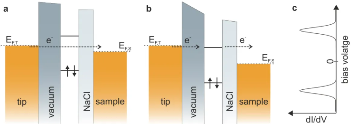
As mentioned above, STS opens up the possibility to characterize the electronic structure of individual molecules and to resolve their frontier orbitals. However, molecules that are adsorbed on a metallic surface exhibit a large level broadening due to hybridization with the metal surface [6]. In 2005 Repp and coworkers showed that this electronic coupling to the supporting substrate can be avoided by using a few monolayers (ML) thin insulating NaCl separation layer [6]. Due to the large band gap of NaCl a strong hybridization of a molecule’s frontier orbitals is prevented, whereas tunneling through such thin NaCl films occurs at rates that enable STM operation [6].
STM on such ultra-thin films can be described in the picture of a double barrier tunneling junction, as shown in Fig. 2.2. Here, tip and sample correspond to the two metal electrodes, and the vacuum gap and the NaCl layer correspond to the two tunneling barriers, separating the molecular levels from the two electrodes. EF,T and EF,S refer to the Fermi level of tip and sample, respectively. For simplicity, it is assumed that the work functions of the tip and the sample are identical. The molecular states are indicated as discrete levels, however, in practice these levels generally experience a broadening of ≈300 meV due to coupling of molecular states to phonon modes of the NaCl film [25].
tip sample
EF,T
vacuum NaCl tip sample
EF,S
vacuum NaCl
e- e-
EF,T
a b
e-
EF,S
bias volatge
dI/dV c
0
Figure 2.2: Tunneling through a double barrier tunneling junction. a Direct tun- neling at small voltages (in gap). b Sequential tunneling through an unoccupied molecular state in resonance with the Fermi level of the tip.
Electrons can tunnel from the tip into a molecular state, which is rapidly emptied via tunneling of the electron to the sample. cIdealized differen- tial conductance curve.
2.2 Atomic Force Microscopy By applying a positive bias voltage to the sample with respect to the tip, the Fermi levels are shifted relative to each other such that electrons from occupied states in the tip can tunnel into empty states at the surface. At a small bias voltage (Fig. 2.2a), no unoccupied states are available in the molecule, and electrons can only tunnel directly from the tip to the sample. If the bias voltage is large large enough that the Fermi level of the tip aligns with an unoccupied molecular state, electrons can resonantly tunnel from the tip to a molecular level to the sample (Fig. 2.2b). The additional possibility of resonant tunneling through a molecular level, gives rise to a peak in the conductance dI/dV at the corresponding voltage (Fig. 2.2c).
Similarly, at a sufficiently large negative sample voltage, tunneling from the sample via occupied molecular levels into free states in the tip can occur, also giving rise to a peak in differential conductance at negative bias voltage.
2.2 Atomic Force Microscopy
In 1986 Binnig, Quate, and Gerber introduced the atomic force microscope (AFM) [2].
Analogous to STM, an atomic-scale sharp tip is used to scan a surface. Instead of measuring tunneling currents, the working principle of AFM is based on the detection of the tiny forces that act between a tip, which is mounted to a flexible cantilever, and the sample surface. A force, acting between tip and sample, will cause a deflection of the cantilever. This force can be determined by measuring the cantilever deflection.
Since AFM is based on measuring forces, it is not limited to conductive materials, thereby enabling the atomic-scale surface investigation of insulating materials.
An AFM can be operated in several different modes. The simplest one is the static mode, where the tip-sample force is directly determined from the static deflection of the cantilever. However, in static AFM the interacting forces between tip and sample can lead to a jump-to-contact, which occurs because of the requirement to use very soft cantilevers in order to measure tiny forces [26, 27].
For non-destructive measurements with ultimate resolution, it is required to oper- ate in a dynamic mode, where the cantilever is externally driven to oscillate at or close to its resonance frequency. In general, there are two methods for dynamic operation, namely, amplitude-modulation (AM) and frequency-modulation (FM) mode [26]. Throughout this thesis, we exclusively used FM-AFM. Hence, only this operational mode will be discussed in the following. FM-AFM was first proposed by Albrecht et al. [29] and its operating principle is shown Figure 2.3a.
In this mode, the cantilever is driven to oscillate at its resonance frequency f0, and when being brought close to a surface, the interaction with the surface causes a mea- surable frequency shift ∆f. For this operational mode, several external circuits are necessary which will be described in the following. The deflection of the cantilever is recorded and amplified. A phase-locked loop detects the frequency shift with respect to the resonance frequency f0 of the unperturbed cantilever. Additionally, an auto- matic gain control is used to keep the cantilever oscillating at a constant oscillation
x,y sample
tip-sample force z
a
oscillating cantilever automatic gain control phase locked loop
dissipation
amplitude Δf
excitation multiplier
f+Δf
b
m
sample k
kTS
xyz-control preamplifier tip
tip height
Figure 2.3: a Schematic picture of the operation principle of an AFM in frequency modulation mode. b Mass and spring model of cantilever and tip-sample forces. After [28].
amplitude. To this end, the output signal of the automatic gain control and the resonance frequencyf+ ∆f are multiplied, and applied as an excitation signal to the cantilever [28, 29]. Analogous to STM, there are two common operational modes. In constant-height mode the tip is scanned in a plane parallel to the sample surface, to map the local frequency shift variations.
Alternatively, the AFM can be operated in constant-∆f mode, where the tip-sample distance is adjusted by an additional feedback loop to maintain a cantilever oscillation at constant amplitude at a predefined ∆f set point.
In the following, it will be derived how the frequency shift relates to the forces that act between tip and sample according to reference [28]. As illustrated in Fig 2.3b, the oscillating cantilever can be considered as a mass m∗ attached to a spring with an effective stiffness k and hence its unperturbed resonance frequencyf0 is given by
f0 = 1 2π
r k
m∗ . (2.7)
The force Fts arising from the tip-sample interaction potentialUts can be considered as an additional spring of stiffness kts attached to the tip,
Fts =−ktsz , (2.8)
wherekts =−∂F∂zts is the effective spring constant, andz the tip-sample distance. This approximation is only valid in the limit of small cantilever oscillation amplitudes, for which kts can be assumed as constant within the range of the cantilever oscillation
2.2 Atomic Force Microscopy (for the experiments, shown in this thesis, the oscillation amplitude was ≤ 2 ˚A).
Under this assumption, the resonance frequency of the perturbed cantilever may be expressed as
f = 1 2π
rk+kts
m . (2.9)
If it is further assumed that k >> kts, f can be written as f =f0
1 + kts 2k
. (2.10)
This is justified since our AFM cantilevers have stiffnesses ofk = 1800 N/m[28], while tip-sample stiffnesses are typically below 10 N/m . Hence, the frequency shift ∆f can be given as
∆f =f−f0 ≈f0kts
2k0 =− f0 2k0
∂Fts
∂z = f0 2k0
∂Uts2
∂z2 . (2.11)
Equation 2.11 shows that the measured frequency shift is proportional to the gradient of the force that acts between tip and sample and hence proportional to the second derivative of the tip-sample interaction potential Uts.
In general, there are several types of forces, with different decay lengths that can act between the tip and a surface [28]. For resolving the structure of individual molecules, the relevant forces are the rather long-range attractive van der Waals forces and short range Pauli repulsion [9]. The interaction potential corresponding to these force contributions is often empirically modeled with a Lennard-Jones potential [28, 30].
Further, electrostatic forces play a crucial role for detecting charge states of atoms or molecules and charging events by means of AFM [11, 31]. Thus, their role will be discussed in more detail in the next section.
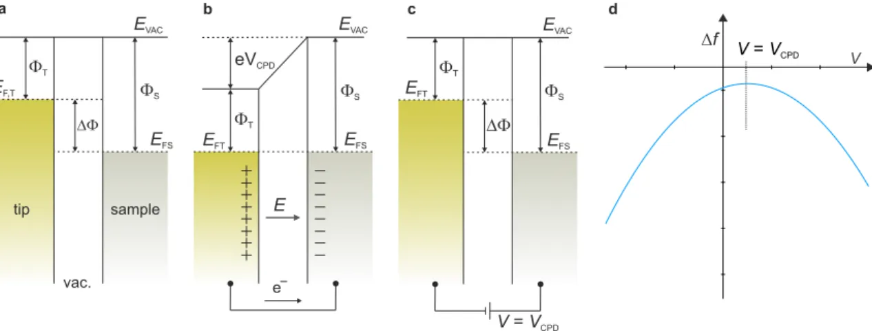
2.2.1 Kelvin probe force spectroscopy
Kelvin probe force spectroscopy (KPFS) is a method by which local variations of the sample work function can be detected. It is related to the Kelvin Probe method, which was first reported by Lord Kelvin in 1898 [32]. In this technique, two metals plates of different materials, which are in electrical contact, are being brought close.
If the distance between these plates is modulated at a frequency ω the capacitance periodically changes, causing an alternating current between the two plates. The resulting current is minimized if an additional bias voltage is applied between the two plates that equals the contact potential difference of the two metal plates [33]. This can be rationalized in the following picture, where the tip and sample are considered as the two metal electrodes with distinct work functions ΦT, ΦS, as shown in Fig. 2.4.
For the electrodes being not in electric contact, the difference between their Fermi levels is given by their difference in work functions ∆Φ = ΦT −ΦS (Fig. 2.4a).
Upon electric contact formation, charge carriers will flow from the electrode with the
a
FS
DF FT
sample EVAC
EFS
EF,T FS
FT
EVAC
EFS
EFT
FS
DF FT
EVAC
EFS
EFT
vac.
eVCPD
V = VCPD
e
b c
tip E
V = VCPD V d
Δf
Figure 2.4: Principle of KPFS. a Tip and sample before electric contact formation.
b Tip and sample in electric contact. Surface charges accumulate upon alignment of the Fermi levels, which gives rise to an electrostatic force.
c A voltage VCP D is applied to compensate for this electrostatic force.
d Schematic ∆f(V) curve. The electrostatic force contribution becomes minimal atV =VCP D. Figure after [34].
lower work function to the one with the larger work function until their Fermi levels align (Fig. 2.4b). This gives rise to an electrostatic potential commonly referred to as contact potential differenceVCP D = ∆Φ/eand hence to an electrostatic force between the electrodes. This contact potential difference and the resulting electrostatic force can be compensated by applying a bias voltage V = VCP D between the electrodes (Fig. 2.4c). Hence, for the case of the Kelvin Probe method, the current will go to zero if the contact potential is compensated.
Instead, KPFS relies on the sensitivity of AFM to electrostatic forces. In the fol- lowing, it will be briefly explained how the electrostatic force and the resulting fre- quency shift depend on the applied voltage. If the curvature of the tip is neglected, tip and sample can be described as a plate capacitor, with tip and sample as the two plates [33]. If one takes into account the contact potential difference between tip and sample, the energy Uel stored in the capacitor is given by
Uel = 1
2C(z) (V −VCP D)2 , (2.12) where z denotes the tip-sample distance, C the tip-sample capacitance and V the applied bias voltage. According to eq. 2.11 the dependence of the frequency shift, arising from electrostatic forces, on the applied bias voltage reads as
∆fel∝ ∂Fel
∂z ∝ ∂Uel2
∂z2 ∝ 1 2
∂C2
∂z2 (V −VCP D)2 . (2.13) From this relation, one can see that the frequency shift has a square dependence
2.2 Atomic Force Microscopy of the applied bias voltage. Hence, the electrostatic contribution to the measured frequency shift becomes minimal, when the applied sample voltage equals theVCP D. In KPFS, the frequency shift ∆f is recorded as a function of the applied bias voltage, which is schematically shown Figure 2.4d. The horizontal shift of the minimum of the parabolic curve gives the contact potential difference between tip and sample.
Nonnenmacher and colleagues first applied the principle of minimizing the electro- static forces to AFM, when they proposed the method of Kelvin Probe Force Mi- croscopy [35]. This method allowed them to detect local work function differences while at the same time recording topographic images of a surface by means of AFM with a spatial resolution below 50 nm.
This opended the door to the distinction of different charge states of atoms and molecules [11, 12, 14, 15, 36] and even to the detection of subtle work function vari- ations caused by a non-homogeneous distribution of charges within single molecules by means of KPFS [37–39].
Since AFM measures contact potential differences with high spatial resolution, the voltage needed to compensate the contact potential difference (VCP D) is often referred to as local contact potential difference (LCPD).
2.2.2 Dissipation
Dissipative forces will be important for the interpretation of the results presented in chapter 6. Therefore, a brief introduction into their role in FM-AFM will be given and what physical origins can potentially give rise to dissipation in experiments.
A freely oscillating cantilever can be described as a weakly damped harmonic oscil- lator, and hence its energy loss per oscillation cycle ∆Ecantilever is given by
∆Ecantilever = 2πE
Q, with E =kA2
2 , (2.14)
where E is the energy stored in a cantilever oscillating at an amplitude A, k its stiffness and Q the quality factor [26, 28]. When the AFM tip is brought close to a surface, tip-sample forces arise. In FM-AFM, conservative forces lead to a change in the resonance frequency, whereas non-conservative forces cause dissipation [26, 40]. If the tip-sample forces occurring during image acquisition are conservative, the tip-sample force will result only in a frequency shift of the cantilever. Since this intrinsic dissipation of the cantilever depends on fixed parameters, it will not lead to any spatial signatures in AFM measurements, irrespective of local tip-sample force variations.
However, a non-conservative tip-sample force can lead to an additional energy change
∆Ets per cycle [26].
Such a non-conservative tip-sample interaction is schematically shown in Fig. 2.5.
Variations of the force, for example, arising from charging a single molecule [36],
can give rise to abrupt shifts in a measured F(z) curve. Under the condition that charging and discharging occur at different cantilever positions, this will open up a hysteresis in the probed F(z) signal and hence give rise to an increase or decrease in dissipation, depending on the direction of the force shifts.
Hence, ∆Ets per cycle is given by the integral of the tip-sample force Fts along the cantilever pathway within one oscillation cycle [26]
∆Ets = I
Fts(z+q0)dq0. (2.15) This additional contribution will affect the measured dissipation. In general, such dissipative forces can be of different origins. For example, Lotze et al. found that molecular hydrogen trapped between tip and surface can drive an AFM cantilever by inducing motions of the molecular hydrogen via inelastic electron tunneling [41]. Fur- ther, such non-conservative forces can arise from variations of the electrostatic force during a cantilever oscillation cycle. This was exploited in the group of Grutter, for example, to map single-electron charging events of quantum dots [42–44]. Ondr´aˇcek, Hapala and Jel´ınek, simulated how such perodic charge modulations affect the can- tilever dynamics [45]. Further, Steurer and colleagues examined the relation between tunneling rate and dissipation for the sequential tunneling through vacancy states in
Force
0
Tip-sample distance, z 2 A0
ΔE
oscillating cantilever
Figure 2.5: Cantilever dissipation due to non-conservative forces. The vertical range of cantilever motion is defined by the cantilever oscillation amplitude (width of grey shaded area). The orange area corresponds to the dissi- pated energy. Arrows indicate trajectory of the force curve.
2.3 Charge transfer processes in SPM NaCl [46]. Recently, we made use of dissipative forces to image molecular orbitals on insulators [36].
In our experimental setup, the dissipated energy is not directly measured, instead the excitation signalA is recorded that is needed to keep the cantilever oscillate at a constant amplitude. However, it can be derived that the microscopic dissipation can be quantified by relating the measured excitation signal A to the excitation of the unperturbed cantilever A0, using [26, 28]
∆Ets = 2πE Q
A−A0 A0
. (2.16)
2.3 Charge transfer processes in SPM
Since charge transfer processes play a central role in all the experiments presented in this thesis, a brief literature overview of charge state manipulation and detection by means of SPM will be given. Further, the concept of Marcus reorganization energy [47], which is an important mechanism for charge stabilization, will be briefly explained.
In 2004 Repp and colleagues investigated individual Au atoms adsorbed on an ul- trathin decoupling NaCl layer, grown on a Cu(111) substrate, by means of STM [7].
They found that the charge state of Au atoms can be switched by applying voltage pulses and, moreover, that the atoms exhibit charge bistability, which means that an atom can stably exist, either, in its neutral or singly negative charge state within a certain range of the applied bias voltage [7]. Shortly after, such bistability was also observed for single molecules by Wu et al. [48, 49], Leoni et al. [50], and Swart et al.[8].
Further, it was found by Olsson and colleagues [51] and Steurer and colleagues [31]
that atoms can be stable in three different charges states on thin NaCl films.
Since the early 1990s several pioneering studies have appeared that demonstrated the capability of AFM to measure charge state transitions with single electron sensitiv- ity [52–56]. In 2009 Gross et al. demonstrated that AFM can even resolve different charge states of individual Au atoms, adsorbed on ultrathin insulating films by means of KPFS [11].
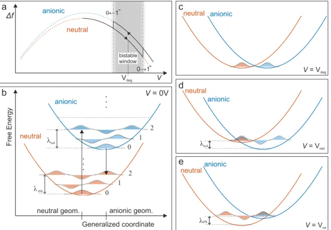
As discussed in section 2.2.1, the measured ∆f signal has a square dependence of the applied bias voltage. Upon charging, the electrostatic contribution to the force will change. Furthermore, the additional charge will affect the local work function and hence distinct charge states are assigned to distinct parabolic ∆f(V) curves [11].
Such parabolic curves are schematically shown in Fig. 2.6a for two distinct charge states as dashed red and blue curves. The horizontal shift of the parabolas is related to the change of the LCPD due to the additional charge. However, the vertical shift is in many cases difficult to interpret and can not straightforwardly be assigned to a difference in electrostatic forces [31]. For example, vertical relaxations of the probed
atom or molecule upon charging can also account for a vertical shift of a ∆f(V) curve. In AFM measurements, such charge state transitions appear as distinct steps in ∆f(V) due to the fact that each charge state is assigned to a distinct parabolic curve [11, 31]. Such a charging spectra is schematically depicted as a solid black curve in Fig. 2.6a, with a hysteresis due to charge bistability.
The aforementioned studies on charging single adsorbates were predominantly car- ried out for adsorbates on thin insulating films [7, 8, 31, 48–51], where the tunnel coupling to the conductive substrate is very large and hence a transiently occupied state would in most cases be immediately emptied. However, if the electron affinity of an adsorbate is close to the Fermi level of the substrate, a transiently occupied state can shift across the Fermi level of the substrate, and hence be stabilized, due geometrical relaxations of the adsorbate and the NaCl film as a response to the ad- ditional charge in the adsorbate [7, 8, 51]. This energy gain upon relaxations of the molecular geometry and its environment is commonly known as Marcus reorganiza- tion energy [47, 57–60].
Beyond experiments on ultrathin films, where charge bistability is only possible with certain restrictions, AFM enabled to investigate charge state transitions for mole- cules adsorbed on insulating substrates, where tunneling is only possible between tip and molecule [14, 15, 60].
Following reference [60], the concept of reorganization energy for a single molecule can be explained in a Franck-Condon picture. As shown in Fig. 2.6b, each charge state is attributed to a distinct potential energy curve with corresponding vibra- tional states. The horizontal axis refers to the generalized coordinate, which takes into account the geometric structure of the molecule and its environment. The un- derlying idea of the Franck-Condon principle is that electronic transitions occur fast compared to the timescales of nuclear motions, for which reason only vertical transi- tions are allowed [61]. This picture is often used in the context of optical spectroscopy, where these vertical transitions correspond to the absorption and emission of photons.
There, both curves represent electronic states with the same number of electrons.
In contrast, here, transitions require an electron exchange with the tip. Therefore, the free energies of the two charge states have to be considered with respect to elec- tron exchange with the tip and thereby the free energy curves are shifted vertically with respect to each other by the applied bias voltage.
At the voltage Vdeg that corresponds to the degeneracy of the neutral and anionic vibrational ground states, a charge transfer is very unlikely due to the weak spatial overlap of the vibrational wave functions (wave functions of the nuclear coordinates - see Fig. 2.6c). If the bias voltage is increased further (V =Vred, Fig. 2.6d), the vibra- tional ground state of the neutral molecule energetically aligns with an vibrationally excited anionic state, whose vibrational wave function has a significant spatial overlap with the vibrational wave function of the neutral molecule, and hence a charge state transition can occur with significant probability. Once being charged, the molecule- substrate system relaxes into the anionic vibrational ground state. The resulting energy gain is called relaxation energy λred[60].
2.3 Charge transfer processes in SPM
Generalized coordinate
Free Energy λred
λox
neutral geom. anionic geom.
λox
λred V = Vred
V = Vox
V = 0V
V = Vdeg
neutral anionic
b
e d c
neutral anionic
anionic neutral neutral
anionic
Vdeg
Δf
V neutral
anionic
a
bistable window
0→1- 0←1-
0
0
2 1
2 1
Figure 2.6:aSchematic picture of an electron transfer processes as observed in AFM
∆f(V) spectroscopy experiments. The solid curve indicates a ∆f spec- trum and dashed curves correspond to the parabolic ∆f curves of two distinct charge states. b-e Electron transfer in a Franck-Condon Picture.
bFree energy curves of a molecule in the neutral an anionic state and the corresponding vibrational modes, without applied bias voltage. c Both charge states are brought to degeneracy by an applied bias voltage Vdeg. d Reduction occurs if a transition between the neutral vibrational ground state and an vibrational state of the anionic molecule, with significant spatial overlap, becomes energetically allowed (V =Vred). e Similarly, at V =Vox oxidation takes places if the anionic vibrational ground state en- ergetically aligns with an excited neutral state with significant vibrational wave function overlap. The figure was adapted from [60].
Fully analogous, the discharging can only occur with significant probability if the anionic vibrational ground state energy intersects with a neutral state with a large overlap of the respective vibrational wave functions, being accompanied by a re- laxation energy λox (V = Vox, Fig. 2.6e). The reorganization energy is defined as Ereorg =λox+λredand is responsible for the hysteretic nature of the charge transfer in single molecules [60]. For adsorbates on NaCl, this reorganization energy was re- ported to be in the order of 1 eV [7, 60].
In experiments, however, we observe that the hysteresis can be much narrower than one would expect from those values. Furthermore, the width of the observed hystere- sis reduces with reduced tip-sample distance and ultimately collapses. The reason behind this is that the strength of the tunnel coupling to the conductive electrodes is not taken into account in the above model. If this tunnel coupling becomes large, charge transitions can even occur at V = Vdeg. Further taking into account that all the levels exhibit a broadening of ≈ 300 meV [25], it becomes clear that the transi- tions voltagesVoxandVredare not discrete values but underlie a certain stochasticity, for which reason the transitions of the bistable window are indicated as blurred in Fig. 2.6a. Hence, the observed hysteresis width must not be directly interpreted as a measure for the reorganization energy, but rather reflects the product of tunnel coupling and reorganization energy.
2.4 Alternate-charging scanning tunneling microscopy
The use of insulating films as a decoupling layer [6] has become indispensable for the investigation of the electronic structure of individual molecules in scanning probe mi- croscopy. Especially AFM allowed to gain fascinating insights into electron transfer processes at the single-molecule scale [12, 14, 31, 60]. To access such out of equilib- rium charge states, in most cases, a thick insulating NaCl film is required to suppress charge transfer to the conductive substrate. Thereby, the characterization of the electronic structure by means of STM is inhibited.
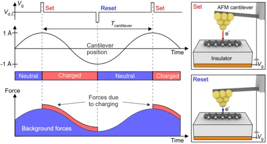
Recently, we developed a novel imaging technique that enables the mapping of molec- ular orbitals on insulators with atomic-scale resolution, which is called alternate- charging scanning tunneling microscopy (AC-STM) [36, 62–64].
Figure 2.7 shows the working principle of this technique. The d.c. bias voltageVd.c. is chosen to lie within the bistable window of a certain charge state transition of a mol- ecule to be investigated (compare Fig. 2.6a). By applying suitable voltage pulses of opposite polarity (Set and Reset, t ≈100 ns), synchronized with the AFM cantilever oscillation, the charge state is periodically switched. Importantly, the phase of the pulses with respect to the cantilever motion is chosen such that theSet pulse occurs at the upper and the Reset pulse at the lower turnaround point of the cantilever.
This results in different electrostatic forces acting on the cantilever during up- and downward movement and, hence, causes a measurable dissipation of the cantilever motion [36].
The key to spatial resolution is the exponential nature of tunneling. Given an ampli- tude of A = 1 ˚A the tunneling probability at the upper turnaround point is reduced by a factor of ≈100. In experiments, the tip height is chosen such that the efficiency of switching the charge state of the molecule with the Reset pulse is one irrespective of the spatial tip position above the molecule. In contrast, the efficiency of switching the charge state with theSet pulse is strongly reduced since it occurs at significantly larger tip height. Hence, theSetpulse becomes sensitive to the spatial orbital density,
2.5 AFM with functionalized tips and thereby enables to obtain images of the latter based on the spatial modulation of tunneling probability.
For a detailed description of the experimental technique and its applications, it is referred to [36, 62, 64].
Background forces Background forces
Set Reset Set
Neutral Charged Neutral Charged
1 Å
-1 Å
Tcantilever
Forces due to charging
Set
Reset
AFM cantilever
Insulator e
e Vd.c.
Vg
Vg
Vg Cantilever
position Time
Time Force
-
-
Figure 2.7: Working principle of AC-STM. Pulses of opposite polarity (Set,Reset) are used to charge and discharge a molecule, synchronized with the oscillatory motion of the cantilever. This causes periodic changes of the measured force thereby leading to an increase in dissipation. The schematic pictures indicate the direction of electron transfer corresponding to the Set and Reset pulses. The figure was adapted from [36].
2.5 AFM with functionalized tips
In 2009 Gross et al. demonstrated that AFM can be used to resolve the chemical structures of single molecules [9]. To this end, a single carbon monoxide (CO) mole- cule was transferred to apex of the tip. When imaging individual molecules with such a CO-functionalized tip, sharp lines appear in the AFM image contrast that resemble the chemical structure of the probed molecule. This technique has become a pow- erful tool for resolving the chemical structure of individual molecules at the atomic scale and enabled characterizing of on-surface reactions [65–71] adsorption geome- tries [72, 73], and even distinguishing bond orders within a single molecule [10, 12].
It was found that the observed intramolecular contrast in such images originates from Pauli repulsion, arising from the overlap of electron densities of the CO mol- ecule at the tip and the probed molecule at the surface at very small tip-sample distances [9, 30]. Van-der-Waals (vdW) forces, instead, only lead to a featureless attractive background signal, due to their long-range nature [9, 30]. Further, Hapala et al. found that the low lateral stiffness of the CO molecule at the tip leads to
an additional contrast sharpening and the observation of sharp ridges in the image contrast that have a close resemblance to chemical structure drawings [74]. However, those sharp ridges can not always be simply interpreted as actual bonds. Instead, they could also result from the specific interaction potential landscape, as shown in studies by Pavliˇcek et al. and H¨am¨al¨ainen et al. [75, 76]. The fact that the CO molecule easily bends at the tip due to the tip-sample interactions can give rise to strong distortions of the apparent molecular structure in AFM images [74, 76, 77].
Apart from CO, several other tip functionalizations have been reported to be useful for specific aspects of AFM. For example, M¨onig et al. found that an oxygenated copper tip enables much less distorted imaging of individual molecules [78]. Further, Br-terminated tips were reported to be useful for lateral manipulation of molecules on an insulating surface, and Xenon tips were recommended for KPFS measurements by Mohn and colleagues [79].