Chapter 5
Semiconductor-based detectors: An introduction
Most of today’s detectors of light used in astronomical instruments are based on semicon- ductors. In this chapter the very basics of such technology is reviewed. A more in-depth and broad treatment will be given by A. Quirrenbach lateron in the course. And R. van Boekel will discuss the practical issues an observer will have to deal with when using CCDs and related technology.
Literature:
P. L´ena, F. Lebrun, F. Mignard, “Observational Astrophysics”
C.N. Kitchin, “Astrophysical Techniques”
F. Graham Smith, T.A. King and D. Wilkins, “Optics and Photonics”
5.1 Conductors, insulators, semi-conductors
In an isolated atom, the electron quantum states have discrete energies. All electrons are clearly associated (bound) to this single atomic nucleus. In a molecule, the low-lying electron levels are still bound to their respective atom, but the levels in the outer shell (called the valence shell) may be shared by neighboring atoms. This leads to covalent bonds, i.e. molecular bonds. However, the electrons in one molecule are still isolated from any neighboring molecules. As a result of this localization, the electron energy levels are still discrete energies.
In metals, however, the valence electrons are shared by all atoms in the metal. Each valence level splits into a (semi-) infinite number of sub-levels, creating a valence band.
The different energies within this band are associated to different momenta (movement) of the electrons, or in other words with different!k of their wave functions. Metals are good conductors because the electrons in these valence bands are not fixed to their atoms. But that is not the only condition for conduction. What makes a metal a conductor is that if you apply an external electric field to it (a potential difference), the electrons will start to accelerate and move. Normally, the probability distribution of !k of the electron “cloud”
has zero average: !!k" = 0. If you apply an electric field E, the electrons start moving on! average a bit more in the direction of −E. That is:! !!k" becomes non-zero. In quantum terms this means that electrons start to, on average, occupy higher |!k| states. This is,
Conduction band Conduction band
Conduction band
Conductor Semiconductor Insulator
E
Conductor Valence band
Valence band Valence band
Valence band
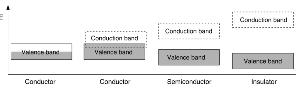
Figure 5.1: Energy diagrams of metal-like materials. Left two panels: conductive metals.
Far right: insulator. Mittle-right: semiconductor. For the insulator and the semiconductor the energy difference ∆E between the valence and conduction bands are called the band gap.
however, only possible if there are such states available. If each state of the valence band is occupied, then no such !k-adjustment can take place. In such a case, in spite of the electrons being delocalized, the solid is an insulator.
There are two ways a metal can be a conductor (Fig. 5.1, left two panels). One is that its valence band is only partially filled. Since electrons have always two spin states, each band has at least the possibility of being 0% filled, 50% filled or 100% filled. In the 50%
case there is sufficient “space” left for the electrons to adjust their !k in response to an external potential. Another possibility is if you have overlapping bands. While the valence band might be 100% filled, electrons can also occupy the lower states of the next higher energy band if this band energetically overlaps with the valence band. Such a band is called the conduction band. The lower part of this conduction band have the same energy as the upper parts of the valence band. In this case there is also plenty of “space” for electrons to adjust their states.
Going back to the example of the insulator: Also insulators have higher-energy “conduc- tion bands”, but they do not energetically overlap with the (filled) valence band (Fig. 5.1, right two panels). There is aband gap between the valence and conduction bands. If the band gap ∆E is large compared to the temperature of the material, i.e. if ∆E $kT, then the chance that en electron gets “accidently” thermally excited to the conduction band is so low that this virtually never happens. That is why such a material is an insulator.
However, for materials with a very shallow band gap, where ∆E ! kT, the conduction band is easily thermally filled. These materials do conduct. For intermediate cases, with
∆E still substantially larger than kT, but still small enough that thermal excitation (or absorption of a photon!) can every now and then excite an electron from the valence band into the conduction band, we have low but not zero conductivity. Such materials, where the conductivity depends on thermal or photon excitation of electrons into the conduction band, are called semiconductors.
The most well-known semiconductor is Silicon (Silicium). Pure silicon can exist in metallic (amorphous) form or in crystalline form. It has a band gap energy ∆E = 1.12 eV at 300 K, which amounts to ∆E/kT = 43 at this temperature, meaning that indeed not many of the electrons are expected to be in the conduction band.
However, suppose that some other process excites electrons into the conduction band, for instance the absorption of a photon. We then have a mobile electron that contributes to conductivity. But we also have a positively charged vacancy, called a “hole”. The hole can
acceptor
semiconductor donor semiconductor
Conduction band Conduction band
E
p−type n−type
Valence band Valence band
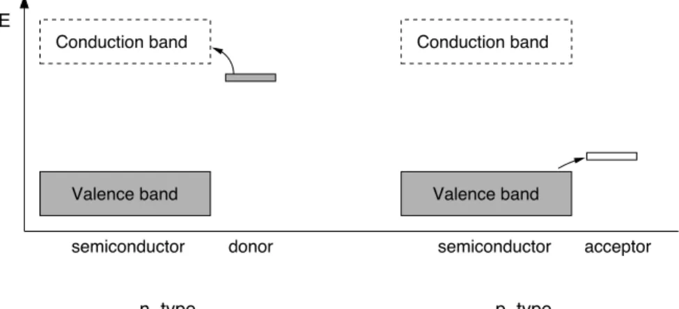
Figure 5.2: Energy diagrams of doped semiconductors (called “extrinsic semiconductors”).
In each of the two panels the left bands are those of the semiconductor (note: the vertical scale is now scaled up compared to Fig. 5.1), and the right band is the energy level of the valence shell of the dopant. In the left case we get an n-type semiconductor. In the right case we get a p-type semiconductor.
now also move around, as if it is a positively charged particle in itself. If an electric field is applied to the material, the free electrons in the conduction band move in −E! direction while the holes move in +E! direction. Both movements contribute to the conduction.
5.2 Doping of semiconductors: n-type and p-type
A semiconductor like silicon has a band gap that is large enough that thermal excitations of electrons from the valence band into the conduction band are rare at room temperature.
However, even very tiny amounts of pollutants may act as electron donors or acceptors.
Consider injecting phosphorous atoms into a silicon crystal, one phosphorous atom for each 106 silicon atoms for instance. This process is calleddoping, and phosphorous acts as a dopant. The average distance between two phosphorous atoms, in this example, is then about 100 silicon atoms in the silicon lattice. Phosphorous happens to have a valence shell energy that is very close to the lower energy of the conduction band of silicon. This means that ∆E between the phosphorous valence shell and the silicon conduction band is much smaller than the ∆E of the silicon band gap (see Fig. 5.2-left). At room temperature the electrons of phosphorous occupying this state can thus easily get thermally excited into the conduction band of silicon. The electron is now free to move. This dopant thus acts as a donorof an electron. The hole, however, is stuck to the phosphorous atom. Since the next phosphorous atom is about 100 silicon atoms away, there is no chance that this hole can tunnel to the next dopant atom. These dopant holes are therefore immobile and do not contribute to the conduction. In such a situation we thus have one current carrier only:
the electrons. Such a doped semiconductor is called ann-type semiconductor, because the conduction is provided by negatively charged particles.
Consider now instead to dope the silicon with Boron, in an equally rarified amount.
Boron has a valence shell energy that is slightly above the upper bound of the valence band of silicon, and this energy level is still unoccupied (see Fig. 5.2-right). Thermal fluctuations can now easily inject a silicon valence band electron into this shell. The dopant acts thus
as a acceptor of an electron and becomes negatively charged. This negative charge is now fixed to the boron atom and is immobile. The hole in the valence band of the silicon, however, is now mobile and contributes to the conductivity of the semiconductor. Such a doped semiconductor is called ap-type semiconductor, because the conduction is provided by positively charged “particles”: the holes.
Both n-type and p-type semiconductors are conducting reasonably well, each in their own way. Such semiconductors are calledextrinsicsemiconductors. Non-doped pure semi- conductors are called intrinsic semiconductors or i-type semiconductors. Typically one must make semiconductor materials extremely pure (apart from the dopants of course) in order to get the proper behavior.
5.3 The photoconducting effect and the dark current
It was already briefly mentioned that apart from thermal fluctuations, also the absorption of a photon can put an electron into the conduction band. This property is extremely useful for making detectors of light. The simplest of these principles is to simply measure the conductivity of a piece of i-type semiconductor as light falls onto it. This is simply done by applying a voltage over the semiconductor and measuring the current. The more light is absorbed, the more electron-hole pairs are produced and the larger the current will be. This is called the photoconducting effect. A detector of this kind can only measure photons that have hν ≥∆E of the band gap. For silicon, with ∆E = 1.12 eV, the longest wavelength that can be measured is thus λ=1.1 µm. Visible light is thus well within this range.
If your semiconductor is of n-type, the ∆E between the dopant and the conduction band is much smaller than thus much longer wavelength photons can be measured. Typ- ically you would like to have pretty strong doping, so that the chance of a photon being detected is large (goodquantum efficiency). But too many dopant atoms would destroy the semiconducting property. A special class of detectors, theblocked impurity band detectors (BIBs), tries to separate the two spatially, thus aquiring the best of both.
However, for such doped semiconductors sensitive to long wavelength ratiation, also thermal excitation becomes much more of a problem. Even without photons reaching the semiconductor there would then be a current due to the thermal excitation. This is called the dark current. It is therefore important to cool the detector to very low temperatures to reduce the dark current to low enough levels that meaningful observations can be made.
The temperature down to which you have to cool is in fact not much dependent on the type of detector: it depends on physics, on the ratio hν/kT. You want this ratio to be large enough that thermal noise is not going to disturb your sensitive measurements.
Since in astronomy we are always looking for the weakest signals, you can imagine that even for optical astronomy you may want to cool your detector.
5.4 p-n Junctions and the photovoltaic effect
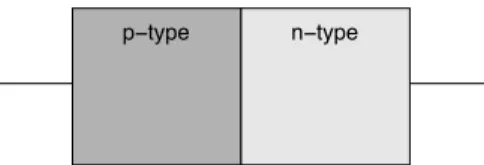
One of the most basic building blocks of modern electronics is thep-n junction (Fig. 5.3).
It a p-type semiconductor and an n-type semiconductor are joined at an interface (the p-n junction) one obtains a diode: current can be made to flow in the direction from p
p−type n−type
Figure 5.3: Schematic view of a p-n junction.
to n, but not from n to p. One can see this in the following way. If we put a potential difference on the junction with positive slope from p to n (abackward bias), then the holes in the p semiconductor will be pushed away from the junction, and the electrons in the n semiconductor will also be pushed away from the junction. The region around the junction thus becomes devoid of current carriers (it becomes “depleted”) and no current can flow.
Reversing the potential (a forward bias) would push the holes toward the junction, and the electrons as well. At the junction the electrons and the holes will recombine so that no charges build up. There will be no depleted zone and a current can continue to flow. By the way, the recombination of holes and electrons at the junction produce photons: this is how a light emitting diode (LED) works.
There is, however, another interesting effect at a p-n junction. Suppose we do not add any external potential. Then there is no force pushing the holes or the electrons anywhere.
But there is still the thermal diffusive motion of the holes and electrons. This means that some electrons will randomly stray into the p-type semiconductor and will there recombine with the holes. Likewise the holes may randomly stray into the n-type semiconductor and recombine with the electrons. This means that even without an external potential there will be a thin depletion layer around the junction. As this layer becomes thicker due to continuing diffusion, a potential builds up, because in the absense of holes in the p- type junction we are left with the negatively charged dopants which are immobile, and on the n-side in the absense of the electrons we are left with the positively charged dopants which are also immobile. This charge separation will lead to a potential difference across the junction which starts to counteract the diffusion. At some point an equilibrium is obtained where the diffusion is quenched by the potential difference. This sets the width of the depletion zone.
Now consider what happens if a photon ejects an electron out of the valence band in the depletion zone into the conduction band (photoelectric effect). Due to the strong electric field the electron is pushed toward the n-type semiconductor while the hole is pushed toward the p-type semiconductor. These new charges create now a minor opposing potential. The original potential difference across the junction was an equilibrium state and would not be able to drive a current in a circuit. But the opposing potential difference by the mobile charges produced by the photoelectric effectdoes produce a potential difference that can lead to a current. So by measuring this current one measures the amount of photons that have interacted with the junction. This is called the photovoltaic effect. One could in fact tap energy from this current, and this is the way a solar cell works.
5.5 MIS capacitors: Detecting photons one-by-one
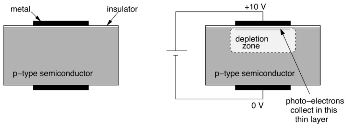
Metal-Insulator-Semiconductor(MIS) capacitors, or its subclassMetal-Oxide-Semiconductor (MOS) capacitors, are photon detection devices that can measure and store information of
insulator metal
0 V +10 V
p−type semiconductor p−type semiconductor
depletion zone
photo−electrons collect in this
thin layer
Figure 5.4: Schematic view of a MIS or MOS type capacitor, which stands at the basis of CCD technology for electronic photography. Left: the structure of a MIS/MOS device.
Right: when a voltage (a “bias”) is applied.
the number of photons that have passed through the device during an exposure to light.
They form the basis of CCD technology described below.
The idea is to have a layered structure with a metal anode or cathode on top, a semiconducting material on the bottom and a thin layer of insulating material separating the two. This is the MIS structure. If the insulating layer is simply a layer of oxide (e.g.
SiO2) then it is called a MOS structure. On the very bottom we would again have a metal cathode/anode, so that the cathode/anode pair can induce a potential difference across the semiconductor.
Suppose we choose an p-type semiconductor for this construction. The mobile charges are holes. If we now put a positive voltage, say 10 V, on the top metal (keeping the bottom metal at 0 V), then the mobile holes in the n-type semiconductor will be pushed away from the positive anode. The region below the 10 V anode will thus become depopulated: it will be devoid of charge carrying holes.
Now consider a photon entering the device and creating an electron-hole pair inside the depopulated region. Because this region has a strong electric field pointing away from the anode, the electron will be rapidly pulled toward the anode, while the hole is pushed away deeper into the semiconductor. Due to the thin layer of insulating material, however, the electron gets stuck just below the anode. In will stay there for as long as the voltage is kept on the device. Every photon of the right energy that enters the semiconductor and creates an electron-hole pair adds an electron to this thin negative charge layer right below the anode. Once we wish to read out how many charges have been collected there, “all” we have to do is to measure somehow the potential induced by this layer of electrons. Once we release the voltage on the anode, the electrons can recombine with the holes and we can start over again.
A MIS or MOS is thus a device that measures the integrated amount of light that has fallen onto the device during some integration time τ. This makes for interesting and extremely useful properties. Such a device has a pretty good linear response. It is very sensitive, having a high quantum efficiency (the ratio of detected photons over incident photons). Also, it allows for long integration times.
p−type semiconductor
No. 1 No. 2 No. 3
measuring device for the charge
Figure 5.5: Schematic view of a CCD: Each pixel has 3 electrodes. By putting the elec- trodes (1,2,3) successively at e.g. (10,2,2), (2,10,2) and (2,2,10) volts and repeating this N times (where N is the number of pixels in this row) one can move the electrons that have collected below the insulator layer in all the pixels to the right where they can be successively read out.
5.6 Charge-Coupled Devices (CCDs): Destructive read- out
Typically a MIS chip is divided into many square zones, each zone being a pixel of the image you want to make. Since we ideally want to have many pixels (high resolution image), we will thus have a huge amount of such zones that we need to read out. Therefore, the read-out of such devices is a non-trivial matter. The charge coupled device is a read-out scheme that has turned out to be very succesful. The idea is that each “pixel” has not one, but three anodes (Fig. 5.5). Let us call these three electrodes 1, 2 and 3. Only one of them is put at a high voltage, the other two at a much smaller voltage. If we start with electrode 1 at high voltage, then all collected electrons in each pixel will be located just below electrode 1 in their respective pixels. If we now gradually increase the voltage on electrode 2 (again in each pixel), then the charges spread out between electrodes 1 and 2. Now reduce the voltage on 1, and all charges move below electrode 2. They have thus moved 1/3 of a pixel. Repeating this in the obvious way two times more will move the charges a full pixel widths. The entire “image” is thus shifted 1 column to the right. At the very right of the CCD we collect the charges on a column of cells which have their 3 electrodes arranged from top to bottom instead of left to right. We can now do the same trick for this collection column and move the charges down to a single point on the CCD.
At this single point we collect the charges, amplify them and create a digital signal of it that is proportional to the number of electrons we picked up. Once the column is empty, we go back to shifting the entire image again one column to the right and again empty the collection column. In this way we have turned a 2-D image into a 1-D sequence of numbers, each representing the charge collected on a pixel.
While this mechanism of readout has been very succesful, there are also some typical problems. One is that if a single pixel is somehow bad (due to manufacturing errors), then all the pixels to the left will have to pass through this pixel, and may thus be affected too.
This will give a horizontal stripe on your image originating at the bad pixel. Likewise a
very strongly exposed pixel may not be perfectly shifted during the readout process, thus also affecting neighboring pixels. Furthermore, any camera based on MIS or MOS pixels can have hot pixels, cold pixels, or can be hit by a cosmic ray (giving a bright pixel) etc.
And because manufacturing of CCDs is a difficult process, the response of pixels is not perfectly the same in all pixels: There can be pixel-to-pixel variations as well as gradients in sensitivity over the image. However, with proper data reduction techniques most of these effects can be removed.
The CCD was originally designed as a form of computer memory, but that application has never become practical. Currently, the word CCD stands for the combined photon collection and readout device. CCDs are used in many astronomical instruments, and are also the chips used in consumer electronic digital cameras.
5.7 Direct Voltage Readout (DVR): Non-destructive read-out
One of the main disadvantages of CCDs is that once you read it out, the signal is lost.
This is so-calleddestructive readout. For long integrations you can thus not have a look at intermediate results. More importantly, you cannot measure the charges multiple times to decrease read-out noise. It would be much nicer if one can measure the charge collected at each pixel simply by measuring the voltage without destroying the charge itself. This is, however, technically much harder to realize. But such deviced exist, and are often used in infrared detectors. For instance, the HAWAII-2 focal plane array (FPA) developed by Rockwell and the Institute for Astronomy in Hawaii is a 2048x2048 pixel near infrared array with direct non-destructive read out. One can address each pixel individually with two registers. This detector is based on HgCdTe material and is sensitive in the λ= 1−5µm wavelength range and has physical pixel sizes of 18x18 µm. By being able to read out a pixel multiple times you can reduce the readout noise.