Klausur zur Vorlesung Schaltungstechnik
TU Berlin, Sommersemester 2011, 22.07.2011
Name (Nachname, Vorname):
Matr.-Nr.:
Studiengang:
BSc / MSc / Diplom:
Erasmus- oder Gast-Student/in:
Ja Nein
Aufgabe: Punkte:
1 / 18
2 / 20
3 / 42
4 / 16
5 / 24
Gesamt: / 120
Note: Datum: Unterschrift:
Aufgabe 1:
Gegeben ist der folgende logische Ausdruck:
x1 x2 x3 x1 x2 x3 x2 x3 x4 x1 x2 x4 x2 x3 x4 x1 x3 x4
y
a) Setzen Sie diesen Ausdruck direkt (d.h. ohne Optimierung / Vereinfachung) in eine Schaltung um, welche aus Invertern, NAND-Gattern und NOR-Gattern (mit beliebig vielen Eingängen) besteht.
4
b) Berechnen Sie die Anzahl der benötigten Transistoren der Schaltung aus a). Gehen Sie davon aus, dass für die Inverter und Gatter-Schaltungen Standard-CMOS-Logik verwendet wird.
2 c) Zeichnen Sie ein KV-Diagramm, welches den oben angegebenen Ausdruck
repräsentiert.
Ermitteln Sie aus diesem KV-Diagramm einen logischen Ausdrucks für y (Achtung: gefragt ist nach dem Komplement der oben angegebenen Funktion, nicht nach y !). Falls sinnvoll, optimieren Sie den erhaltenen Ausdruck weiter. Skizzieren Sie die entsprechende Schaltung.
Verwenden Sie dazu Inverter, NAND-Gatter und NOR-Gatter.
6
d) Entwerfen Sie eine Schaltung ausschließlich aus Invertern und NAND-Gattern, die den logischen Ausdruck für y aus Aufgabenteil d) realisiert.
Geben Sie dazu einen mit den De-Morgan‘schen Gesetzen umgeformten logischen Ausdruck an und skizzieren Sie die erhaltene Schaltung.
4
e) Erweitern oder modifizieren Sie die Schaltung aus Aufgabenteil d), um den oben angegebenen Ausdruck y zu realisieren? Welche Maßnahme oder Änderung ist dazu notwendig. (Antwort in Textform oder durch Angabe eines Schaltbildes).
2
Summe: 18
Englisch Translation:
Consider the logic expression given below:
x1 x2 x3 x1 x2 x3 x2 x3 x4 x1 x2 x4 x2 x3 x4 x1 x3 x4
y
a) Transfer this expression directly (i.e. without optimization / simplification) into a circuit diagram using inverters, NAND gates, and NOR gates (with an arbitrary number of inputs).
4 b) Calculate the number of transistors used in the circuit diagram developed in a). Assume that
standard CMOS logic is used to realize the inverters and logic gates.
2 c) Sketch a KV diagram representing the given logic expression.
On the basis of this diagram develop a logic expression for y (Note: requested is the complementary logic expression with respect to logic expression given above, not y !). If reasonable further optimize the achieved expression. Sketch the related circuit diagram. For this purpose use inverters, NAND and NOR gates.
6
d) Design a circuit using inverters and NAND gates only to realize the logic expression for y developed in part d).
For that purpose provide an adopted logic expression using De-Morgan’s laws and sketch the related circuit diagram.
4
e) Extend or modify the circuit achieved in part d) to realize the expression for y as given above?
Which change is required for this purpose? (Solution can be provided as a short text or by means of a circuit diagram).
2
Sum: 18
Aufgabe 2:
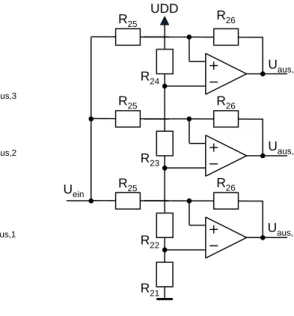
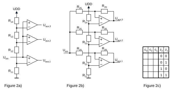
Gegeben ist die in Abbildung 2a) skizzierte Schaltung aus drei Komparatoren und einem Spannungsteiler R1 … R4. für die Generation der jeweiligen Schaltschwellen der Komparatoren. Die positive Betriebsspannung der Komparatoren UDD beträgt 5 V, die negative Betriebsspannung USS ist mit Massepotential identisch (= 0 V). Die angelegte Eingangsspannung Uein kann Werte zwischen Massepotential und UDD annehmen.
a) Die Schaltschwellen der jeweiligen Komparatoren sollen 0.25 UDD, 0.5 UDD und 0.75 UDD betragen, R11 = 10 k. Berechnen Sie bzw. geben Sie die Werte an der Widerstände R12, R13
und R14.
2
b) Skizzieren Sie die Ausgangsspannungen der Komparatoren Uaus,k mit k = 1, 2, 3 als Funktion von Uein in einem Diagramm. Tragen Sie dabei quantitative Werte (d.h. Spannungen in V) an den Achsen auf.
2
c) Die an den Ausgängen der Komparatoren erhaltenen Spannungen können als (5 V-kompatible) Logiksignale interpretiert werden mit
ck = 1 wenn Uaus,k = UDD = 5 V und ck = 0 wenn Uaus,k = USS = 0 V für k = 1, 2, 3 Tragen Sie diese Signale in die in Abbildung 2c) gegebene Tabelle ein. Die erste Zeile soll die Situation für Uein = 0 V darstellen, die folgenden Zeilen alle anderen Möglichkeiten für steigende Werte von Uein.
2
d) Konstruieren und skizzieren Sie eine Logikschaltung, die die drei logischen Ausgangssignale der Komparatoren (c1, c2, c3) in die in den beiden zusätzlichen Spalten der Tabelle angegebenen logischen Signale z1 und z2 umcodiert.
Geben Sie die logischen Ausdrücke für z1 und z2 an und skizzieren Sie eine geeignete Schaltung.
Es können alle Ihnen bekannten Gatter verwendet werden.
4
e) Die Schaltung aus Abbildung 2a) wird nun so erweitert, dass jeder Komparator eine Hysterese aufweist (Abbildung 2b)). Die jeweiligen Schaltschwellen sollen nun liegen bei Uein = 1.25 V ± 10 mV, 2.5 V ± 10 mV, 3.75 V ± 10 mV (d.h. 1.24 V und 1.26 V, …).
Dimensionieren Sie die Widerstände R26 unter der Bedingung R25 = 100 , und geben Sie die Werte der Widerstände des Spannungsteilers R21 … R24 unter der Bedingung R21 + R22 + R23 + R24 = 40 k an, so dass das gewünschte Verhalten erreicht wird.
10
Summe: 20 (English translation see next page)
Uein
Uaus,1 R26
Uaus,2 Uaus,3 UDD
R26
R26 R25
R25 R25
R22 R23 R24
R21 Uein
Uaus,1 Uaus,2 Uaus,3 UDD
R12
R11 R13 R14
c3 c2 c1 z2 z1 0 0 0 1 1 0 1 1
Abbildung 2a) Abbildung 2b) Abbildung 2c)
English Translation:
Consider the circuit given in Figure 2a) consisting of three comparators and a voltage divider R1 … R4 to generate the switching thresholds of the respective comparators. The positive supply voltage UDD equals 5 V, the negative supply voltage USS is at ground potential (= 0 V). The input voltage applied can have values between ground potential and UDD.
a) The threshold voltages of the respective comparators shall be 0.25 UDD, 0.5 UDD und 0.75 UDD, R11 = 10 k. Calculate and provide the values of the resistors R12, R13, and R14.
2
b) Sketch the comparators‘ output voltages Uaus,k with k = 1, 2, 3 as a function of Uein using a diagram. Provide quantitative values (i.e. voltages given in V) at the diagram axes.
2
c) The voltages achieved at the outputs of the comparators can be interpreted as (5 V compatible) logic signals with
ck = 1 if Uaus,k = UDD = 5 V and ck = 0 if Uaus,k = USS = 0 V for k = 1, 2, 3
Add these signals to the table given in Figure 2c). The first row reflects the situation for Uein = 0 V, the following rows provide all further possibilities for increasing values of Uein.
2
d) Design and sketch a logic circuit which transfers the logic output signals of the comparators (c1, c2, c3) into the code provided in the two additional columns of the table with signals z1 and z2.
Provide the logic expressions for z1 und z2 and sketch a suitable circuit.
All types of logic gates are allowed to be used.
4
e) The circuit given in Figure 2a) is now extended in a manner that every comparator provides hysteresis (Figure 2b)). The respective switching thresholds shall be Uein = 1.25 V ± 10 mV, 2.5 V ± 10 mV, 3.75 V ± 10 mV (i.e. 1.24 V und 1.26 V, …).
Provide dimensions for the resistors R26 under condition R25 = 100 , and provide values for the resistors of the voltage divider R21 … R24 under condition R21 + R22 + R23 + R24 = 40 k, so that the requested behavior is obtained.
10
Sum: 20
Uein
Uaus,1 R26
Uaus,2 Uaus,3 UDD
R26
R26 R25
R25 R25
R22 R23 R24
R21 Uein
Uaus,1 Uaus,2 Uaus,3 UDD
R12
R11 R13 R14
c3 c2 c1 z2 z1 0 0 0 1 1 0 1 1
Figure 2a) Figure 2b) Figure 2c)
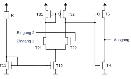
Aufgabe 3:
Abbildung 3 zeigt einen einfachen Operationsverstärker. Die Betriebsspannung UDD beträgt 3.3 V.
Technologie- bzw. Transistorkenngrößen sind Lmin = 0.35 µm, kn = 150 µA / V2, Uth,n = 0.6 V, kp = 60 µA / V2, Uth,p = 0.8 V, n = p = 0.1 / V. Alle Transistoren haben eine Kanallänge L = 1 µm.
a) Identifizieren und benennen Sie bekannte Teilschaltungen. 4
b) Welches ist der invertierende, welches der nicht-invertierende Eingang (kurze Begründung angeben oder skizzieren).
2
c) Berechnen Sie die Weite von T11 (Formel und Wert), so dass T11 mit einer effektiven Gatespannung von 300 mV betrieben und von einem Strom von 54 µA durchflossen wird.
4
d) Berechnen Sie den zugehörigen Wert des Widerstandes R. 2
e) Dimensionieren Sie die Weiten von T12, T21 und T22, so dass der Strom durch jeden Zweig der Eingangsstufe 108 µA beträgt. Alle drei Transistoren sollen die gleiche effektive Gatespannung haben.
2
f) Aufgrund der speziellen Form der Ausgangsstufe soll die Ausgangsspannung der Eingangsstufe bei einer Differenzeingangsspannung von 0 V eine Ausgangsspannung von UDD/2 liefern.
Berechnen Sie unter dieser Bedingung die effektive Gatespannung und die Weite der Transistoren T31 und T32 (Formeln und Werte). Geben Sie die Weite auf 100 nm genau an.
6
g) Bestimmen Sie den maximalen Bereich der Common-Mode-Eingangsspannung unter der Bedingung, dass alle Transistoren der Eingangsstufe (einschl. T12) im Sättigungsbereich betrieben werden.
Geben Sie dazu jeweils eine kurze Skizze (oder Erklärung) und die entsprechenden Spannungswerte an.
6
h) Wählen Sie für T4 die Weite 80 µm. Berechnen Sie die Weite von T5 unter der Bedingung, dass die Ausgangsstufe bei einer Spannung von UDD/2 am gemeinsamen Gateknoten von T4, T5 am Ausgang ebenfalls eine Spannung von UDD/2 liefert. Geben Sie die Weite von T5
auf 1 µm genau an.
4
i) Berechnen Sie die Gesamtleistung der Schaltung, die die Schaltung konsumiert unter der Bedingung, dass alle Transistoren in Sättigung betrieben werden und die Ausgangsspannung UDD/2 beträgt (d.h. unter identischen Bedingungen wie in den Aufgabenteilen e), f) und h) angenommen).
4
k) Geben Sie die Gesamtverstärkung der Schaltung an (Formel(n) und Wert). 8 Summe: 42 (English translation see next page)
R
T21 T22
T11 T12
T5
T4
T31 T32
Eingang 1 Eingang 2
Ausgang
Abbildung 3
English Translation:
Figure 3 shows a simple operational amplifier. Supply voltage UDD is 3.3 V. Technology and transistor parameters are Lmin = 0.35 µm, kn = 150 µA / V2, Uth,n = 0.6 V, kp = 60 µA / V2, Uth,p = 0.8 V, n = p = 0.1 / V.
All transistors have a channel length of L = 1 µm.
a) Identify and name known subcircuits. 4
b) Which input is the inverting one, which one is the non-inverting (sketch or give a short explanation).
2
c) Calculate the width of T11 (equation and value), so that T11 is operated at an effective gate voltage of 300 mV at a current of 54 µA.
4
d) Calculate the related value of resistor R. 2
e) Provide dimensions of the widths of T12, T21 und T22, so that the current through every branch of the input stage is 108 µA. All three transistors shall be operated at same effective gate voltage.
2
f) Due to the particular design of the output stage, the output voltage of the input stage shall be UDD/2 under condition that the differential input voltage is 0 V.
Under this condition calculate effective gate voltage and width of transistors T31 und T32
(equations and values). Provide the width with an accuracy of 100 nm.
6
g) Determine the maximum range of the common mode input voltage under condition, that all transistors (including T12) are operated in the saturation region.
Provide a brief sketch (or explanation) for the respective cases and provide the related values of the voltages.
6
h) For T4, choose width = 80 µm. Calculate the width of T5 so that the output stage delivers a voltage of UDD/2 at ist output under condition that the voltage at the common gate node of T4, T5 equals UDD/2, too. Provide the width of T5 with an accuracy of 1 µm.
4
i) Calculate the total power consumption of the entire circuit under condition that all transistors are operated in the saturation region (i.e. under same conditions as assumed in parts e), f) and h)).
4
k) Calculate the total gain of the circuit (equation(s) and value). 8 Sum: 42
R
T21 T22
T11 T12
T5
T4
T31 T32
Eingang 1 Eingang 2
Ausgang
Abbildung 3
4 3 2
3 x x x
y
4 3 2
3 x x x
y
Aufgabe 4:
Gegeben sind drei logische Funktionen y1, y2, y3. Dabei ist - y1 gegeben durch das unten angegebene KV-Diagramm, - y2 gegeben in Form der unten angegebenen Wahrheitstabelle, - y3 durch die logische Funktion
a) Gesucht ist die Funktion . Geben Sie diese in möglichst einfacher Form an.
8
b) Realisieren Sie die Funktion z ausschließlich durch Verwendung von NAND-Gattern (mit einer beliebigen Anzahl von Eingängen) und von Invertern und skizzieren Sie die Schaltung.
4
c) Realisieren Sie die Funktion z nun ausschließlich durch Verwendung von NAND-Gattern mit 2 Eingängen und von Invertern und skizzieren Sie auch diese Schaltung.
4
Summe: 16
Englisch Translation:
Three logic functions, y1, y2, y3, are given with - y1 defined by the KV diagram depicted below, - y2 defined by the truth table depicted below, - y3 defined by the logic equation
a) Function of interest is . Provide this function in as far as possible simplified form.
8
b) Realize this function by using NAND gates (with an arbitrary number of inputs) and inverters and sketch the related circuit.
4
c) Realize this function now by using NAND gates with 2 inputs and inverters and sketch this circuit, too.
4
Sum: 16
y1: y2:
x1 0 1 1 0
x2 0 0 1 1
x3 x4
0 0 1 1 0 0
1 0 0 0 1 1
1 1 0 1 0 1
0 1 1 0 1 1
y2 x1 x2 x3 x4
0 0 0 0 0
0 1 0 0 0
1 0 1 0 0
0 1 1 0 0
0 0 0 1 0
1 1 0 1 0
0 0 1 1 0
1 1 1 1 0
1 0 0 0 1
0 1 0 0 1
0 0 1 0 1
1 1 1 0 1
1 0 0 1 1
1 1 0 1 1
0 0 1 1 1
0 1 1 1 1
3 2
1 y y
y
z
3 2
1 y y
y
z
Aufgabe 5:
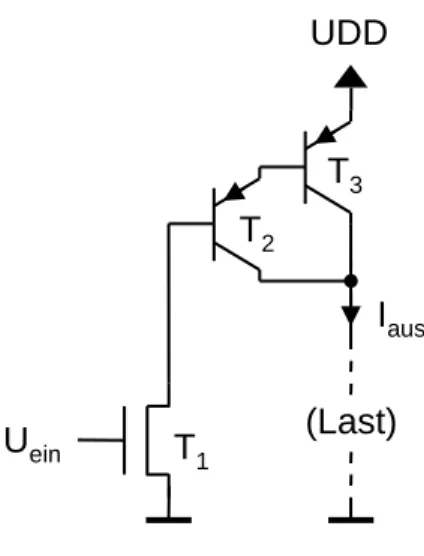
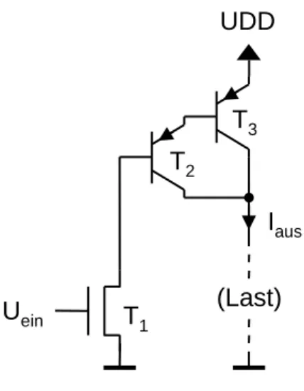
Abbildung 5 zeigt eine einfache spannungsgesteuerte Stromquelle bestehend aus einem n-MOS-Transistor T1 und zwei pnp-Bipolar-Transistoren T2 und T3.
Die Kenngrößen des n-MOS-Transistors sind kn = 110 µA / V2, Uth,n = 580 mV, L = 1 µm, W = 1.5 µm. Für die Bipolar-Transistoren können Sie von einer konstanten Stromverstärkung = 50 und von einem konstanten Basis-Emitter-Spannungsabfall von UBE = 650 mV (Betrag) ausgehen. Die Betriebsspannung UDD beträgt 2.5 V.
Die Abhängigkeit der Kollektorströme von T2 und T3 von der jeweiligen Kollektor-Emitter-Spannung können vernachlässigt werden. Die Abhängigkeit des Drainstromes von T1 von dessen Drain-Source-Spannung kann ebenfalls vernachlässigt werden, sofern T1 in Sättigung betrieben wird.
a) Die Eingangsspannung Uein kann über den Bereich von 0 V bis UDD variiert werden. Geben Sie die minimale Eingangsspannung Uein,min an, die notwendig ist, damit die Schaltung von Strom durchflossen wird.
2
b) Identifizieren Sie die Intervalle der Eingangsspannung Uein, in denen T1 im Sättigungsbereich und im Triodenbereich betrieben wird.
4
c) Berechnen Sie den Ausgangsstrom Iaus als Funktion der Eingangsspannung Uein (Formeln).
Geben Sie den Wert von Iaus an für den Wert von Uein, bei welchem der Arbeitspunkt des Transistors T1 vom Sättigungsbereich in den Triodenbereich übergeht.
Geben Sie ferner den Wert von Iaus an für Uein = UDD.
Skizzieren Sie den Ausgangsstrom Iaus als Funktion der Eingangsspannung Uein.
10
d) Belasten Sie den Ausgang nun mit einem Widerstand R gegen Masse. Geben Sie eine Abschätzung für den Wert von R an (Formel und Wert), der nicht überschritten werden darf, damit die an diesem Widerstand abfallenden Spannung (Uaus) über den ganzen Bereich der Eingangsspannung Uein auch wirklich eine Funktion von Uein ist.
Nehmen Sie bei dieser Betrachtung an, dass der Emitter-Kollektor-Spannungsabfall an den Bipolartransistoren vernachlässigbar klein, jedoch nicht negativ sein darf.
4
e) Skizzieren Sie die zu der angegebenen Schaltung komplementäre Schaltung. 4 Summe: 24 (English translation see next page)
Uein
T2
Iaus UDD
T1
T3
(Last)
Abbildung 5
English Translation:
Figure 5 shows a simple voltage controlled current source consisting of n-MOS transistor T1 and two pnp- bipolar transistors T2 and T3.
The characteristic parameters of the n-MOS transistor are kn = 110 µA / V2, Uth,n = 580 mV, L = 1 µm, W = 1.5 µm. For the bipolar transistors a constant current gain = 50 is assumed and a constant base-to- emitter voltage drop of UBE = 650 mV (absolute value). Supply voltage UDD is 2.5 V.
The dependence of the collector currents of T2 und T3 on the respective collector-to-emitter voltage can be neglected. The dependence of the drain current of T1 on its drain-to-source voltage can be neglected, too, if T1 is operated in the saturation region.
a) The input voltage Uein can vary within the range of 0 V to UDD. Reveal the minimum input voltage Uein,min which is required to make the circuit drive current.
2
b) Identify the intervals of the input voltage Uein where T1 is operated in the saturation region and in the triode region, respectively.
4
c) Calculate the output current Iaus as a function of the input voltage Uein (equations).
Provide the value of Iaus for the value of Uein which coincides with the transition of the operating point of transistor T1 from saturation into triode region.
Furthermore, provide the value of Iaus for Uein = UDD.
Sketch the output current Iaus as a function of input voltage Uein.
10
d) As a load for the output, add a resistor R between output node and ground now. Estimate a value for R (equation and value) which must not be exceeded in order to make the voltage drop at that resistor (Uaus) within the entire range of input voltages Uein indeed a function of Uein.
For this estimation, assume that the emitter-to-collector voltage drop of the bipolar transistors may be negligibly small but not negative.
4
e) Sketch the complimentary circuit with respect to the circuit given in Figure 5. 4 Sum: 24
Uein
T2
Iaus UDD
T1
T3
(Last)
Figure 5