• Keine Ergebnisse gefunden

Materials Chemistry C

N/A
N/A
Protected

Academic year: 2021

Aktie "Materials Chemistry C"

Copied!
11
0
0

Wird geladen.... (Jetzt Volltext ansehen)

Volltext

(1)

Cite this:J. Mater. Chem. C,2017, 5, 4752

Designing 3D topological insulators by 2D-Xene (X = Ge, Sn) sheet functionalization in GaGeTe-type structures†

F. Pielnhofer, *

a

T. V. Menshchikova,*

b

I. P. Rusinov,

bc

A. Zeugner,

d

I. Yu. Sklyadneva,

befg

R. Heid,

f

K.-P. Bohnen,

f

P. Golub,

d

A. I. Baranov,

dh

E. V. Chulkov,

bcgij

A. Pfitzner,

a

M. Ruck

dh

and A. Isaeva *

d

State-of-the-art theoretical studies anticipate a 2D Dirac system in the ‘‘heavy’’ analogues of graphene, free-standing buckled honeycomb-like Xenes (X = Si, Ge, Sn, Pb, etc.). Herewith we regard a 2D sheet, which structurally and electronically resembles Xenes, in a 3D periodic, rhombohedral structure of layered AXTe (A = Ga, In; X = Ge, Sn) bulk materials. This structural family is predicted to host a 3D strong topological insulator with Z

2

= 1;(111) as a result of functionalization of the Xene derivative by covalent interactions. The parent structure GaGeTe is a long-known bulk semiconductor; the ‘‘heavy’’, isostructural analogues InSnTe and GaSnTe are predicted to be dynamically stable. Spin–orbit interaction in InSnTe opens a small topological band gap with inverted gap edges that are mainly composed of the In-5s and Te-5p states. Our simulations classify GaSnTe as a semimetal with topological properties, whereas the verdict for GaGeTe is not conclusive and urges further experimental verification. The AXTe family structures can be regarded as stacks of 2D layered cut-outs from a zincblende-type lattice and are composed of elements that are broadly used in modern semiconductor devices; hence they represent an accessible, attractive alternative for applications in spintronics. The layered nature of AXTe should facilitate the exfoliation of their hextuple layers and manufacture of heterostructures.

Introduction

Surface properties originating from global and crystal-lattice symmetries have attracted a great deal of attention in the past decade.

1

This interest may be fuelled in the foreseeable future by the Nobel Prize in Physics awarded in 2016 for the discovery of topological phases of matter and topological transitions.

Materials hosting 2D and 3D Dirac fermions are believed to foster new types of devices and to complement or even excel classic semiconductor transistors. Over just a few years, various types of topological materials, e.g. topological insulators,

2

topological crystalline insulators and superconductors,

3

non- symmorphic crystalline insulators,

4

Weyl semimetals,

5,6

etc.

have been discovered. Herewith, we suggest a new platform for 3D strong topological insulators: GaGeTe-type layered bulk materials that are structurally related to both basic zincblende- type semiconductors and 2D-Xene materials.

7

The progenitor GaGeTe has been synthesized as bulk crystals.

8,9

It has a layered crystal structure stacked from six- atom-thick

2N

[Te–Ga–Ge–Ge–Ga–Te] building blocks (denoted henceforward as a hextuple layer of GaGeTe) separated by van der Waals gaps. Each hextuple layer can be considered as a buckled two-atom-thick germanium sheet in the armchair

a

University of Regensburg, Institute of Inorganic Chemistry, Universita ¨tsstr. 31, 93053 Regensburg, Germany. E-mail: florian.pielnhofer@ur.de

b

Tomsk State University, pr. Lenina, 36, 634050 Tomsk, Russia.

E-mail: menshikova_t@mail.ru

c

St. Petersburg State University, Universitetskaya nab., 7/9, 199034 St. Petersburg, Russia

d

Technische Universita ¨t Dresden, Department of Chemistry and Food Chemistry, Helmholtzstraße 10, 01069 Dresden, Germany. E-mail: anna.isaeva@tu-dresden.de

e

Institute of Strength Physics and Materials Science, pr. Academicheskii 2/1, 634021, Tomsk, Russian Federation

f

Karlsruher Institut fu ¨r Technologie, Institut fu ¨r Festko ¨rperphysik, D-76021 Karlsruhe, Germany

g

Donostia International Physics Center (DIPC), Paseo de Manuel Lardizabal, 4, 20018 San Sebastia ´n/Donostia, Basque Country, Spain

h

Max Planck Institute for Chemical Physics of Solids, No ¨thnitzer Str. 40, 01187 Dresden, Germany

i

Departamento de Fı´sica de Materiales, Facultad de Ciencias Quı´micas, UPV/EHU, 20080 San Sebastia ´n/Donostia, Basque Country, Spain

j

Centro de Fı´sica de Materiales CFM-MPC, Centro Mixto CSIC-UPV/EHU, 20080 San Sebastia ´n/Donostia, Basque Country, Spain

†Electronic supplementary information (ESI) available: Further details of electronic structure calculations, relaxation of bulk, chemical bonding analysis, QTAIM effective charges and delocalization indices, and short nomenclature discussion.

See DOI: 10.1039/c7tc00390k Received 23rd January 2017, Accepted 18th April 2017 DOI: 10.1039/c7tc00390k

rsc.li/materials-c

Materials Chemistry C

PAPER

Published on 18 April 2017. Downloaded by Universitaetsbibliothek Regensburg on 30/06/2017 10:14:34.

View Article Online

View Journal | View Issue

(2)

configuration wrapped in a four-atom-thick structural fragment of the b-GaSe-type structure.

10

While further relevant structural peculiarities of GaGeTe are detailed in the next section, the immediate discussion focuses on the corrugated germanium fragment. It bears a striking structural similarity to germanene

11

and other 2D monolayers of group IVA atoms (graphene,

12

silicene,

13,14

stanene

15

) that are under intense spotlight nowadays due to the high mobility of charge carriers and are envisioned as components of future transistors. These artificial 2D materials coined Xenes (X = IVA elements), which accommodate X atoms in the buckled honey- comb arrangement, are predicted to exhibit the quantum spin Hall effect (QSHE), possibly even persisting up to room temperature.

7

Furthermore, some proposals advocate that topological states emerge in the covalently functionalized Xane derivatives. For instance, a 2D topological insulator is expected in halogen- functionalized germanane GeX (X = H, F, Cl, Br), methyl- substituted GeCH

316–18

and ethynyl derivatives of germanene GeC

2

X (X = H, halogen)

19

under sizeable tensile strain. Ethynyl- or methyl-functionalized stanene

20,21

and halide-functionalized plumbene

22

exemplify the case of heavier elements. On the other hand, ionically functionalized Xene-like structural fragments in Zintl compounds MX

2

(M = Ca, Sr, Ba; X = Si, Ge, Sn) may account for an entire family of topological materials ranging from topological nodal-line semimetals to presumably Dirac semimetals and even a strong topological insulator with Z

2

= 1;(001) in BaSn

2

, as has been very recently found by first-principles calculations.

23–25

Experimental confirmation of these perspectives has been so far strongly challenged.

7

An impressive achievement is the recently reported synthesis of germanane GeH, a hydrogen-saturated analogue of graphane,

26,27

that has been obtained via hydrolysis of the bulk b-CaGe

2

precursor.

28,29

GeH is a trivial wide-gap semiconductor with a band gap of 1.56 eV,

16

and its electronic structure can be flexibly varied by chemical pressure so that the band gap size changes by ca. 15%.

30

Herewith, we demonstrate by means of a first-principles study that covalent functionalization of an Xene-like structural fragment may implicate topological order in the bulk GaGeTe- type structure. Up to now, scarce characterization of the physical properties

31–33

and the absence of any band-structure calculations have kept GaGeTe away from the mainstream research. We aim to fill in this gap and to entice further experimental verification of the predicted properties.

The present contribution focuses on the electronic structures of bulk GaGeTe and its hypothetical, isostructural analogues, GaSnTe and InSnTe, with stronger spin–orbit coupling. While the latter compounds are predicted to be topological materials on all levels of theory applied (DFT, screened hybrid functional, GW correction), the case of the forerunner remains inconclusive.

Being a narrow-gap TI within DFT, GaGeTe is rendered a trivial semiconductor with a much larger band gap by the HSE06 functional and the GW-approach. Lately, theory has helped to identify many TI candidate materials with the aid of the Z

2

classification,

34–37

and ensuing experiments confirmed or disproved these predictions for a considerable number of

‘‘contenders’’.

2

In the course of that pursuit, the problem of

false-positive TI prospects churned out by DFT calculations was identified and the rather resilient GW-method was proposed to ameliorate it.

38,39

Noteworthy, the hybrid HSE functional, which is traditionally regarded as superior to the standard DFT ones, was also found to yield false-negative results in the search for new TIs, as opposed to DFT and GW calculations.

38

Thus, the contradictory theoretical predictions for GaGeTe urge experimental efforts such as transport measurements and spectroscopy studies for ultimate clarification.

Methods

Electronic structures

Electronic structure calculations were carried out within the framework of density functional theory (DFT). Various program packages were used complementarily in order to verify the obtained electronic properties.

Structural optimizations and calculations of the AXTe (A = Ga, In; X = Ge, Sn) band structures were performed using the projector augmented-wave (PAW) method

40

as implemented in the VASP (Vienna ab initio simulation package) code.

41–43

In the VASP code, the exchange–correlation energy was treated using the generalized gradient approximation (GGA) with the Perdew–

Burke–Ernzerhof (PBE)

44

parametrization. Scalar-relativistic corrections were included in the Hamiltonian and the spin–

orbit coupling (SOC) was taken into account by the second variation method.

45

A k-point mesh of 7 7 7 was used after the preliminary tests showed that an increased mesh did not affect the obtained spectra. Bulk relaxation of AXTe was carried out by the DFT+D3 method that correctly describes the van der Waals interactions.

46,47

Furthermore, the topological character of the AXTe electronic structures has been tested by the calculations using the exact exchange functional HSE06

48,49

which includes a Hartree–Fock term in the exchange part. This functional is known to represent the band structures of semiconductors with higher accuracy with respect to DFT.

50

Z

2

invariants were computed via the parities of the wave functions according to the Fu and Kane formalism

51

and by the method implemented in Z2Pack.

52,53

The results obtained by both approaches are in full agreement.

GW calculations were performed using VASP

41–43

and WANNIER90

54,55

codes. In the first stage, DFT calculations employing the PBE functional were performed without including the spin–orbit coupling. For the calculation of the dielectric function, 300 bands were chosen that correspond to an energy window up to 100 eV above the Fermi level. The k-point mesh was chosen to be 7 7 7. The SOC was taken into account using an a posteriori treatment method

39

on the basis of the Wannier interpolation technique.

Furthermore, full structural optimizations were carried out using the linear combination of atomic orbitals (LCAO) method as implemented in CRYSTAL14

56

for GaGeTe as well as for the hypothetical model compounds GaSnTe and InSnTe. Apart from the PBE parametrization plus Grimme’s D2 dispersion correction,

57

local density approximation (LDA) in the Vosko–Wilk–Nusair

Published on 18 April 2017. Downloaded by Universitaetsbibliothek Regensburg on 30/06/2017 10:14:34.

(3)

(VWN)

58

parametrization was applied. The total energy was converged on a k-mesh with 10 10 10 k-points. Besides adjusted all-electron basis sets for Ga (86-4111d41G),

59

Ge (97-631d61G),

60

In (97-63111d631G)

61–63

and Sn (97-63111d631G),

64

an all-electron basis set for Te

65

and a pseudopotential basis set (m-pVDZ-PP) for a scalar-relativistic description of Te

66

were used.

The electronic structures of AXTe were additionally assessed by the full potential local orbital (FPLO) method

67

as implemented in the FPLO program (version 14.00-45). The PBE functional and LDA with the Perdew–Wang (PW91)

68

parametrizations were applied. For GaGeTe, the experimental structure and geometries optimized using the CRYSTAL calculations and FPLO-LDA approach were considered as an input for band structure calculations. The hypothetical GaSnTe and InSnTe structure models were derived solely from the CRYSTAL calculations. A full-relativistic Hamiltonian (Dirac–Coulomb) was applied in the FPLO calculations and the total energy was converged on a k-mesh with 12 12 12 k-points.

Full-potential (L)APW+lo+LO LDA

68

DFT calculations were performed using the ELK code.

69

A scalar-relativistic Hamiltonian by Koelling and Harmon was used.

45

Spin–orbit coupling was taken into account perturbatively in the second variational step and included only the spherical part of the Kohn–Sham potential inside muffin-tin spheres as implemented in the ELK code. A k-mesh of 11 k-points inside the irreducible part of the Brillouin zone for the primitive lattice was used. The RGk

max

parameter and angular momentum cut-off used for the wave function expansion inside the muffin-tin spheres were chosen equal to 8.

Further computational details can be found in the ESI† (Table S6).

The dielectric function and corresponding optical coefficients of GaGeTe were also calculated using the ELK code

69

on the 7 7 7 k-point grid. Preliminary tests showed that an increased k-point mesh and switched-on spin–orbit coupling did not bring in any qualitative changes in the computed dielectric function. The ELK results appeared to be in full accordance with the above-mentioned VASP results.

Projector-augmented-wave GGA

44

calculations were performed using the ABINIT code.

70

Modified ABINIT datasets

71

were used and the plane wave cut-off energy was equal to 20 a.u. Further information on computational parameters can be found in Table S6 in the ESI.†

In terms of the electronic structures, the results of ELK and ABINIT codes were completely in accordance with those obtained by the above-mentioned VASP and FPLO codes. Hence, the results of the former were used further as an input for the analysis of the chemical bonding.

For the calculation of the phonon-dispersion spectra, the electronic structure calculations of GaSnTe and InSnTe were performed using the mixed-basis pseudopotential approach

72

with the exchange and correlation energy functional evaluated within the generalized gradient approximation.

44

Spin–orbit coupling was incorporated into the pseudopotential scheme via Kleinman’s formulation and treated fully self-consistently.

73

Elastic moduli were calculated from the obtained phonon spectra. Phonon dispersions were calculated using the linear response technique

74

in combination with the mixed-basis pseudopotential method.

75

Evaluation of chemical bonding

Evaluation of quantum theory of atoms in molecules (QTAIM) basins was performed

76

using the electron density computed for AXTe (A = Ga, In; X = Ge, Sn) on a discrete grid with a B0.05 a.u. step using the program DGrid.

77

The same code was used to compute the delocalization indices

78–81

between the QTAIM basins from the (L)APW and PAW results.

82,83

Delocalization indices characterize the degree of electron pair exchange between the basins (two atoms) and can be interpreted as the covalent-bond order.

81

For spinor wave functions employed in the calculations including spin–orbit coupling, the delocalization indices were computed according to the method reported in ref. 84.

Additionally, the QTAIM basins were computed for an optimized bulk structure of GaGeTe from the electron densities calculated from all-electron basis sets using the CRYSTAL code and analyzed using TOPOND.

85

The results are fully consistent with those obtained by the above-mentioned method.

ELI-D (electron localizability indicator) is a real-space bonding indicator

86,87

that partitions the crystal-lattice space into non- overlapping regions (basins) designating atomic cores, penultimate valence shells, electron lone pairs and regions of pairwise or multi- centre bonds. Moreover, integration of the electron density within these basins (similar to the QTAIM concept

88

) allows quantifying the electron count for each bond, while the polarity index (p)

89

determines the bond polarity through the ratios between the electronic contributions of all bonding constituents.

Results and discussion

Crystal structures of bulk AXTe (A = Ga, In; X = Ge, Sn) The periodic layered structure of GaGeTe

9

can be understood as a stack of 8.17 Å thick, layered packages with a diamond-like atomic arrangement (Fig. 1). Furthermore, these hextuple layers are stacked with anti-phase boundaries, making it impossible to derive the entire GaGeTe bulk structure from a zincblende-type 3D lattice with regular voids in the 6c Wyckoff site. Instead GaGeTe adopts an ABC stacking sequence of the hextuple layers along the c axis resulting in a trigonal unit cell (sp. gr. R 3m, no. % 166), so the otherwise tetrahedral coordination polyhedron of each Te atom remains incomplete due to the missing vertex (Fig. 1). Like quintuple layers in Bi

2

Te

3

, hextuple layers in GaGeTe are separated by van der Waals gaps of about 3.41 Å (defined as a normal between the adjacent Te atomic planes).

The shortest interlayer Ga Te distances for the atoms in the eclipsed position are equal to 4.670 Å, while the shortest interlayer Te Te distances (van der Waals gaps) amount to 4.131 Å. The prominent layered nature of GaGeTe accounts for abundant stacking faults in the crystals of this material.

32

To the best of our knowledge, isostructural analogues of GaGeTe have not been reported. Since topological order is favoured by stronger spin–orbit coupling, we consider a possibility of isovalent substitutions of germanium and gallium by ‘‘heavier’’

analogues, tin and indium, respectively. Earlier studies of phase equilibria in the A–Sn–Te (A = Ga, In) systems revealed only two quasi-binary sections in each system, e.g., A

2

Te

3

–SnTe and

Published on 18 April 2017. Downloaded by Universitaetsbibliothek Regensburg on 30/06/2017 10:14:34.

(4)

ATe–SnTe, and one stable ternary compound Ga

6

SnTe

10

.

90

Additionally, SnTe-based solid solutions with a rock-salt-type structure are known to incorporate several at% of indium.

Our structural optimization of the unit cell parameters and atomic positions of the hypothetical GaSnTe and InSnTe under a space-group restraint within the DFT+D3 scheme yields plausible interatomic distances and coordination polyhedra (Table 1 and Table S1 in ESI†). The functionalized stanene- like fragment with interatomic Sn–Sn distances of 2.746 Å (GaSnTe) and 2.784 Å (InSnTe) is compressed in comparison with the optimized free-standing 2D-material

18

(2.88 Å) and resembles more the elemental tin (2.81 Å in a-Sn). On the other hand, it is less stretched out than in BaSn

2

(2.919 Å). The degree of buckling in ASnTe (Table 1) accords well with the experi- mental data for stanene on a substrate (ca. 1.2 Å

15

). The A–Te distances in ASnTe (2.752 Å for A = Ga, 2.901 Å for A = In) are widened in comparison with the typical values for the corres- ponding ATe binaries (cf. Ga–Te 2.64–2.69 Å in GaTe,

91

In–Te 2.82 Å in the tetrahedral units in InTe

92

). The most peculiar A–Sn bonding contacts in AXTe echo the rare examples of polyanionic, helical fragments in NaInSn

2

,

93

NaGaSn

294

and NaGaSn

5

.

95

In these Zintl compounds, indium/gallium and tin atoms occupy mixed atomic sites with (distorted) tetrahedral coordination that reside at distances of 2.792 Å (NaInSn

2

), 2.733–2.766 Å (NaGaSn

2

), and 2.763 Å (NaGaSn

5

). LiInSn

96

with a zincblende structure accommodates both In and Sn in the mixed anionic site with an interatomic distance of 2.891 Å.

Along with the credible crystallochemical features, the dynamic stability of the discussed AXTe is corroborated by calculations of their phonon-dispersion spectra

97

and elastic moduli. Positive elastic moduli are one of the parameters indicating a dynamically

stable compound. This requirement is fulfilled for both GaSnTe (C

11

= 37.36 GPa, C

12

= 21.49 GPa, C

44

= 12.31 GPa, C

0

= 7.9 GPa) and InSnTe (C

11

= 36.77 GPa, C

12

= 25.77 GPa, C

44

= 9.9 GPa, C

0

= 5.5 GPa).

To conclude, there is room for justified optimism that the considered ‘‘heavy’’ representatives of GaGeTe-type structures could be synthesized by optimized synthetic routes. As the recent example of layered Ge

4

Se

3

Te shows, even sliced-and-diced systems like Ge–Te and Ge–Se do have structural novelties to unravel.
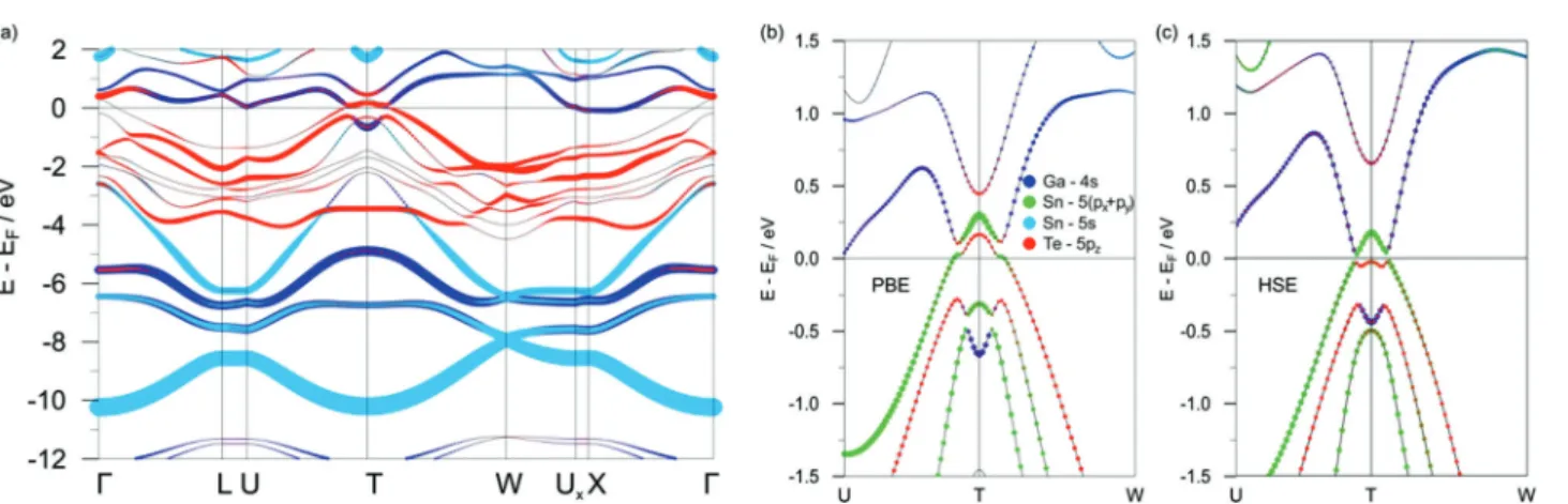
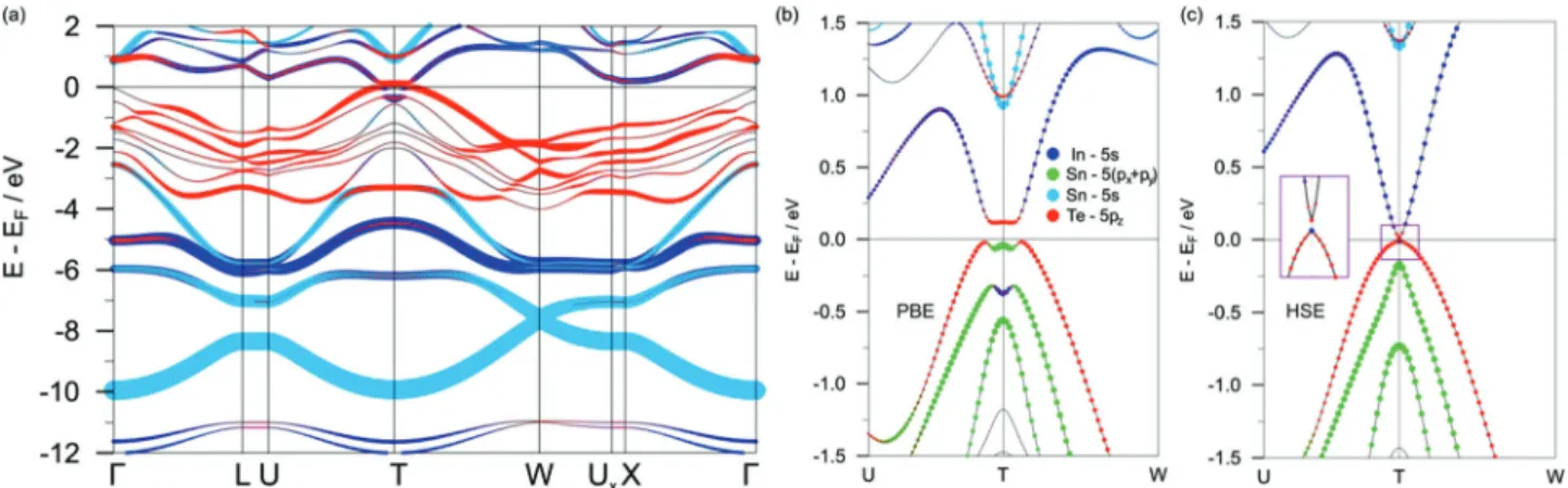
98

Electronic structures of AXTe (A = Ga, In; X = Ge, Sn)

The bulk band structures of AXTe were calculated using a variety of DFT-based codes and exchange–correlation functionals (Table 1). The corresponding geometry optimization data for bulk are summarized in Table S1 in the ESI.† Note that the following discussion is based on the primitive unit cell (rhombohedral setting) which is outlined in Fig. S1 in the ESI.† For structural description (Fig. 1) the conventional unit cell (hexagonal setting) is chosen.

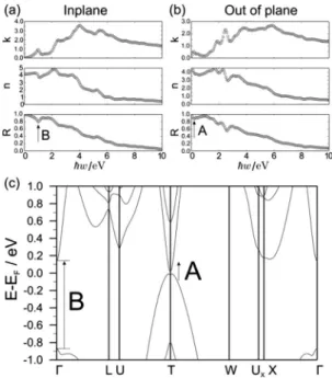
GaGeTe demonstrates a gapless band structure in the scalar- relativistic case (Fig. S2a in ESI†). The valence band (VB) maximum predominantly consists of the Te-5p

z

states, whereas the minimum of the conduction band (CB) has mainly the Ge-4s character. When spin–orbit interaction is taken into account within the PBE functional, the electronic spectrum of GaGeTe gaps out. Four distinct regions with different atomic contributions can be traced in the resultant electronic structure (Fig. 2) and in the projected density of states (Fig. 3a). The top part of the GaGeTe electronic spectrum, the conduction band, is formed by Te p-orbitals, Ga and Ge s-orbitals. The next region, the top of the VB, extends from the vicinity of the Fermi level down to ca. 4 eV. This broad continuum is constituted by strongly intermixed p-states of the tetrahedrally coordinated Ga, Ge and Te atoms with a predominant contribution from the latter. The third region lies between 4 and 7 eV and is characterized mainly by the s-orbitals with a sizeable contribu- tion from the Ga atoms. The last part of the electronic structure at ca. 10 eV is governed by quasi-2D Dirac-cones centered at the W points of the 3D Brillouin zone (Fig. 2a). These states are composed largely of the Ge-4s orbitals; hence they can be attributed to Ge bonding within the buckled layer (Fig. 2b).

The deeper lying Te-5s states represent the non-interacting lone pairs which are typical for layered compounds with van der Waals interactions.

The above-described general characteristics of the GaGeTe electronic structure are not affected in the wide energy range by the choice of exchange–correlation functional or addition of many-body contributions within the GW approximation. The key influence of the chosen functional manifests itself near the Fermi level.

In the framework of the PBE functional, the VB and CB are inverted at the T point of the 3D Brillouin zone and a narrow indirect band gap opens (see Fig. 2c). Its size is quite small due to the moderate hybridization of the states (cf. Table 1). Along the other directions of the Brillouin zone there is a sizeable gap of ca. 2 eV. The topological nature of the resultant semiconducting Fig. 1 Selected views of the bulk GaGeTe structure (conventional unit cell

outlined) with the notions used for the structural fragments in the text. The coordination polyhedra emphasize structural relations with a diamond-like lattice. Note the missing vertex of the Te-centered polyhedron (see text).

DGe defines the buckling of the Ge fragment as a normal between two Ge atomic planes.

Published on 18 April 2017. Downloaded by Universitaetsbibliothek Regensburg on 30/06/2017 10:14:34.

(5)

ground state is identified by the calculation of the four topological Z

2

invariants n

0

;(n

1

n

2

n

3

) as proposed by Fu and Kane.

51

The products of the parity eigenvalues at all time- reversal-invariant-momenta (TRIM) classify the bulk GaGeTe as a strong topological insulator with n

0

;(n

1

n

2

n

3

) = 1;(111) as calculated for the primitive unit cell or, equally, with n

0

;(n

1

n

2

n

3

) = 1;(001) as calculated for the conventional unit cell (see Table S2 in the ESI† for the respective parity eigenvalues at the TRIM points).

Many-body effects are known to have a great impact on the gap edge states in semiconductors. Contradictory to above, calculations using the exact exchange–correlation HSE06 functional yield a dramatically increased band gap of 550 meV in bulk GaGeTe which entails the trivial character of the electronic spectrum (calculated Z

2

= (0;000)). It is also reflected by the changed dispersion of the valence-band edge near the T point (Fig. 2c). Furthermore, the applied GW correction also results in a transition from a topological to a trivial insulator, Table 1 A summary of selected optimized geometrical parameters and electronic band gaps (SOC included) calculated for the bulk AXTe (A = Ga, In; X = Ge, Sn) using various DFT-based codes and parametrisation. Relaxation was performed under a space-group restraint (no. 166), whereas the unit cell parameters and atomic coordinates were allowed to vary. Since structure relaxation cannot be performed using the HSE06 functional in the VASP code, the geometry obtained using the PBE functional was used instead

Computational details

(method-functional) a/Å c/Å V/Å

3

Interlayer d/Å d(X–X)/Å d(X–A)/Å d(A–Te)/Å + X–X–X/ 1 DX/Å Band gap/meV Experimental geometry of GaGeTe

7

FPLO-LDA

a

4.048 34.731 492.87 3.408 2.457 2.442 2.657 110.90 0.759 57

FPLO-PBE

a

29

FPLAPW-LDA

b

70

PAW-PBE

c

33

Optimized geometry of GaGeTe (cf. Table S1, ESI)

FPLO-LDA

a

4.027 34.400 483.16 3.295 2.458 2.415 2.650 110.02 0.797 21

PAW-PBE+D3

c

4.086 34.583 500.11 3.271 2.491 2.451 2.683 110.20 0.800 55

PAW-HSE

c

4.086 34.583 500.11 3.271 2.491 2.451 2.683 110.20 0.800 550

GW 4.086 34.583 500.11 3.271 2.491 2.451 2.683 110.20 0.800 298

Optimized geometry of GaSnTe (cf. Table S1, ESI)

PAW-PBE+D3

c

4.318 35.754 577.33 3.172 2.746 2.631 2.752 103.68 1.151 0

PAW-HSE

c

4.318 35.754 577.33 3.172 2.746 2.631 2.752 103.68 1.151 0

LCAO-LDA/FPLO-LDA

d

4.283 34.984 555.76 3.112 2.706 2.578 2.726 104.65 1.098 0

LCAO-PBE+D2/FPLO-PBE

d

4.296 35.372 565.48 3.123 2.730 2.592 2.743 103.79 1.140 0 Optimized geometry of InSnTe (cf. Table S1, ESI)

PAW-PBE+D3

c

4.482 37.113 645.64 3.111 2.784 2.805 2.901 107.22 1.026 137 (indirect)

PAW-HSE

c

4.482 37.113 645.64 3.111 2.784 2.805 2.901 107.22 1.026 20 (direct)

LCAO-LDA/FPLO-LDA

d

4.450 36.766 630.38 3.069 2.775 2.788 2.871 106.61 1.049 8

LCAO-PBE+D2/FPLO-PBE

d

4.465 37.321 644.35 3.058 2.796 2.819 2.901 105.99 1.082 150 (indirect)

a

FPLO software package.

67b

ELK software package.

69c

VASP software package.

41–43d

Structure optimization using the CRYSTAL code

56

and band structure calculated using the FPLO code. DX defines the height of the buckled germanium/tin fragment (cf. Fig. 1).

Fig. 2 (a) 3D Brillouin zone for the primitive unit cell of GaGeTe. (b) Bulk band structure of GaGeTe with spin–orbit coupling. In panel (c), the bulk band structure calculated within PBE and HSE functionals is enlarged in the vicinity of the Fermi level. The color-coding of the atomic contributions is identical in both panels. Filled circles denote atomic compositions with s- and p

z

-symmetries for the Ga, Ge and Te atoms, respectively.

Published on 18 April 2017. Downloaded by Universitaetsbibliothek Regensburg on 30/06/2017 10:14:34.

(6)

although the band gap expands less drastically (Table 1 and Fig. S2b, ESI†).

The confronting results of the calculations cannot be unequi- vocally juxtaposed with the published transport properties of bulk GaGeTe which raises concerns and requires careful revision.

Optical measurements

32

on GaGeTe crystals with GaTe impurities (documented by X-ray experiments) reported two transmittance maxima at 0.4 and 1.0 eV. The authors ascribed the first one to intraband transitions due to p-doping of the sample and the second one to interband transitions. This finding accords in principle with the earlier mentioned band gap of 1.1 eV

9

that, nonetheless, was not supported by any experimental evidence.

In order to re-interpret the optical experimental investigation,

32

we computed the absorption index (k), refractive index (n), and refractivity (R) on the basis of the dielectric function obtained within the random phase approximation. These quantities derived

from the in-plane and out-of-plane components of the dielectric function are shown in Fig. 4a and b. Two peculiarities at B0.2 eV and B1 eV (denoted henceforward as A and B, respectively) are clearly visible. The former is observed for the out-of-plane component and is poorly resolved, whereas the latter is more pronounced for the in-plane component. The occurrence of these peaks can now be rationalized on the basis of the available GaGeTe band structure (see Fig. 4c). The first peak (A) corresponds to interband optical transitions in the area of the T point. Due to the finite size of the q-point mesh used in our calculations, e.g. 7 7 7, the location of this peak has falsely shifted in the direction of higher energies. Based on this, the transmittance maximum registered at 0.4 eV

32

may be associated with the optical band gap, with a caveat that the earlier interpretation

32

cannot be ruled out either. The second peak (B) can be explained by interband optical transitions near the G point and is in full agreement with the previous experimental observations.

32

The discussed transitions are schematically presented in Fig. 4c. To conclude, our results offer a new interpretation of the experimental data

32

and a plausible explanation of the observed discrepancy between the bandgap estimated from the optical experiment

32

(1 eV) and our computations (55–550 meV dependent on the chosen functional).

If GaGeTe is a trivial semiconductor as found within the HSE functional, artificial augmentation of spin–orbit strength may be considered as a means to evoke a topological phase transition from the trivial insulator into the topological insulator phase.

One possible way to trigger the topological transition could thus be chemical substitution by an isovalent element with a higher atomic number and, respectively, the stronger effective Fig. 3 DOS plots for GaGeTe (a), GaSnTe (b) and InSnTe (c) with the

atomic orbital projected-DOS (full-relativistic FPLO-LDA).

Fig. 4 Absorption index (k), refractive index (n), and refractivity (R) calcu- lated for GaGeTe on the basis of the in-plane (a) and out-of-plane (b) components of the dielectric function. (c) Bulk electronic structure of GaGeTe near the Fermi level. The arrows define the optical transitions corresponding to the peaks in (a) and (b).

Published on 18 April 2017. Downloaded by Universitaetsbibliothek Regensburg on 30/06/2017 10:14:34.

(7)

spin–orbit coupling interaction. In this line of thought, two hypothetical compounds, namely GaSnTe and InSnTe, were further considered. Structural optimisation within the DFT+D3 scheme has confirmed that they are isostructural to GaGeTe.

Tin substitution for germanium resulting in GaSnTe corre- sponds to the increment in the intrinsic spin–orbit strength parameter l

0

from 0.29 (Ge) to 0.8 (Sn).

97

Furthermore, InSnTe possesses the largest effective spin–orbit strength in this series thanks to the l

0

values increasing from 0.174 (Ga) to 0.392 (In).

99

The electronic structure of GaSnTe (Fig. 3b and 5a) considered in the framework of the PBE functional demonstrates strong similarities to GaGeTe in the broad range of energies. For instance, the Dirac cone located at the W point at about 8 eV is in this case formed by the Sn s-orbitals and is thus attributed to the Sn bonding in the stanene-like fragment. Decisively for the present discussion, the bulk band structure of GaSnTe demon- strates qualitative differences close to the Fermi level as it retains the semimetallic character when spin–orbit interaction is accounted for. Moreover, a complex inversion of four bands takes place and involves the Ga s-states, Te p

z

-orbitals, and Sn p

x

- and p

y

-states. This inversion generates several local hybridization gaps between the inverted bands (Fig. 5b). As a result, the emergence of surface states with topological nature can be readily expected which would enable us to classify GaSnTe as a semimetal with topological properties. Similar features were found for the Bi

x

TeI (x = 2, 3) family of topological materials.

100,101

The observed metallic character is maintained with a few minor changes in the vicinity of the T point when the electronic structure is treated by the HSE exact exchange functional (Fig. 5c). Similarly to the PBE case, local hybridization gaps are also found.

As anticipated, in the case of InSnTe (Fig. 3c and 6) the presence of elements with stronger effective spin–orbit coupling interaction with respect to GaGeTe leads to a topological phase transition. Both PBE and HSE exchange functionals concertedly yield an inverted energy gap in the bulk electronic structure of InSnTe. The topological Z

2

invariants n

0

;(n

1

n

2

n

3

) = 1;(111) calculated from the products of the parity eigenvalues at all time-reversal-invariant-momenta (TRIM) and following the method

proposed in Z2Pack

52,53

coincide with those obtained for GaGeTe in the PBE case (cf. Table S2, ESI†). Nevertheless, the size and character of the gap edge dispersion differ significantly for both parametrisations (Fig. 6b, c and Table 1). In the PBE case, an indirect bulk band gap is observed and three bands partake in the complex inversion similarly to the previously discussed GaSnTe spectrum calculated within the PBE functional. The electronic structure of InSnTe obtained in the HSE case is characterized by a direct, small band gap of ca. 20 meV. The gap edges are also inverted but this time only two bands are involved. The analysis of the atomic composition within the HSE functional demonstrates that InSnTe is in proximity to a transition to the trivial phase (Fig. 6c).

Chemical bonding in AXTe (A = Ga, In; X = Ge, Sn) and comparison with functionalized Xenes

Despite notable differences in the electronic structures near the Fermi energy, chemical bonding, as evaluated by means of positional-space bonding analysis, appears very similar in all AXTe (the quantitative results are summarized in Tables S3–S5 of the ESI†). The effective charges of QTAIM atoms indicate electron transfer from gallium/indium to tellurium, while the Ge/Sn atoms remain almost neutral (Tables S3 and S5 in ESI†).

The resultant effective atomic charges for all AXTe generally are in accord with the Ga

2+

Ge

0

Te

2

charge scheme derived earlier

9

from the structural considerations.

Tetrahedral atomic coordination in AXTe signifies strong covalent intralayer bonding between the nearest neighbors as revealed by delocalization indices close to 1, indicating essential electron sharing between the covalently bonded atoms. For instance, d(Ge,Ge) = 0.80, d(Ge,Ga) = 0.73, d(Ga,Te) = 0.70 in GaGeTe, and d(Sn,Sn) = 0.80, d(Sn,In) = 0.70, d(In,Te) = 0.67 (cf. Table S4 in ESI†).

Interactions between more distant atoms are more difficult to analyse since no ELI-D basins are present and the delocalization indices are much smaller. In the following section, the case of GaGeTe is considered in detail. The DI value between the next- nearest Ge atoms (2NN) from the same Ge layer is d(Ge,Ge) = 0.046 (at the distance of 4.048 Å). The DI value between two 3NN

Fig. 5 Bulk band structure of GaSnTe with spin–orbit coupling. The color-coding for the atomic contributions is identical in both panels. Filled circles correspond to the atomic compositions with s-, p

x+y

- and p

z

- symmetries for Ga, Sn and Te.

Published on 18 April 2017. Downloaded by Universitaetsbibliothek Regensburg on 30/06/2017 10:14:34.

(8)

(next-next-nearest neighbors) Ge atoms is one order of magnitude smaller ( d (Ge,Ge) = 0.005 for the distance of 4.736 Å). The observed ratios between the DI values resemble those in diamond (d(C,C) = 0.91 for the first coordination sphere; d(C,C) = 0.039 for the second coordination sphere; d(C,C) = 0.008 for the third coordination sphere)

82,83

as opposed to graphite (the respective values are d(C,C) = 1.20, 0.058 and 0.038).

82,83

These findings highlight the similarity between the buckled germanium layer in GaGeTe and GeH and are consistent with the semiconducting behavior of GaGeTe.

As it follows from the charge analysis, the buckled Ge/Sn fragment within the hextuple layers of AXTe can be placed alongside Xanes

7

as yet another example of Xene functionalization.

Notably, the geometrical characteristics of the germanium sheet (interatomic distances, bonding angles and buckling) are almost identical in GaGeTe and GeH, and bear salient structural similarities to the respective fragment in the Zintl compound b -CaGe

2

which acts as a precursor for germanane

28

(Fig. 7 and Table 2). Similar tendencies are observed in the series InSnTe (GaSnTe)–SnH (stanane)

102

–BaSn

2

(Table 2), although it should be noted that stanane has not been experimentally characterized yet. On the other hand, the chemical bonding scenarios differ in these series of compounds; we again depict it in the example of germanium. The negatively charged germanium sheet with slightly longer Ge–Ge distances and more pronounced buckling than in germanene (cf. Table 2) is incorporated in an ionic

arrangement of Ca

2+

cations in b-CaGe

2

, whereas its analogue is covalently functionalized in GeH and GaGeTe. Two types of functionalizations entail prominently different electronic properties.

Ionic functionalization in b-CaGe

2

results in a semimetallic ground state, whereas germanane which is covalently functionalized via hydrogenation is a topologically trivial wide-gap semiconductor,

16

and its band-gap size can be flexibly varied by chemical pressure up to 15%.

30

Similarly, stanane

103

is expected to be trivial, whereas halogen-functionalized stanene

102

is theoretically predicted to be topological. In GaGeTe, which exhibits covalently bonded, almost neutral germanium sheets sandwiched between the Fig. 6 Bulk band structure of InSnTe with spin–orbit coupling. The color-coding for the atomic contributions is identical in both panels. Filled circles correspond to the atomic compositions with s-, p

x+y

- and p

z

-symmetry for In, Sn and Te, respectively.

Fig. 7 Layered fragments of crystal structures of b-CaGe

2

,

108

(left) and GaGeTe (right) compared to germanane GeH (center). Atomic coordinates of GeH are taken from ref. 28 and 29. The Xene (i.e. germanene in this case) fragment is highlighted in yellow colour. Its geometrical characteristics are summarized in Table 2 together with the respective data on stanene.

Table 2 Comparison of geometric characteristics of germanene/

stanene-like structural fragments incorporated in selected 2D Xanes, Zintl phases and AXTe materials. The degree of buckling DX is defined as a normal between two X atomic planes

Material d(X–X)/Å + X–X–X/ 1 DX/Å

Germanene-like structural fragment

b-CaGe

2108

2.519 104.6 1.02

GeH

28,29

2.435 109.8 0.80

GaGeTe

9

2.457 110.9 0.76

Stanene-like structural fragment

BaSn

2

2.919 105.66 1.14

SnH

109

2.88 — 1.2

GaSnTe (this work) 2.746 103.68 1.15

InSnTe (this work) 2.784 107.22 1.03

Published on 18 April 2017. Downloaded by Universitaetsbibliothek Regensburg on 30/06/2017 10:14:34.

(9)

GaTe fragments, a non-conducting ground state is realized.

Given the stronger spin–orbit coupling interaction, like in InSnTe, a transition into the topological state may occur.

Unlike the considered GaGeTe-type compounds with formally neutral hextuple layers, topological Zintl phases MX

223–25

(M = Ca, Sr, Ba; X = Si, Ge, Sn) are bound to uncompensated surface charge upon cleaving, which interferes with the observations of the topological states by e.g. transport measurements. These hindering effects were examined in detail, for instance, for a weak topological insulator built by alternating charged layers.

104

Hence, GaGeTe-type topological materials may be much easier to handle than Zintl phases.

Conclusions

First-principles calculations identify GaGeTe-type periodic structures as a potential host for topological phases. The layered InSnTe bulk material is predicted to be a 3D strong topological insulator with Z

2

= 1;(111). Unlike structurally related Xenes (2D TI) or stanene-based BaSn

2

(3D TI), whose valence and conduction bands are dominated by atomic-orbital contributions of the buckled honeycomb structural fragment, the complex band inversion in InSnTe, as found within the PBE functional, is realized by the In-5s, Sn-5s and Sn-5p states of the Xene-like sheets and the SOC-split Te-5p states. Thus, covalent functionalization of the Xene-like building block in the periodic 3D stack of GaGeTe-type struc- tures implicates a topological state. Experimental confirmation is urgently called for hypothetical GaSnTe and InSnTe materials which are shown to be dynamically stable.

As far as the series of forerunner GaGeTe is concerned, transport experiments and spectroscopy studies are currently underway to confront the contradictory theoretical predictions.

The measurements on GaGeTe appear feasible thanks to its high stability in contrast to air-sensitive Zintl compounds and artificial 2D materials. In contrast to germanane which quickly becomes amorphous above 75 1 C,

28

GaGeTe offers both thermal (melts peritectically at 800 1 C

9

) and chemical (resistant to air, water and NaOH(aq)

9

) stability.

Although the tetrahedral atomic coordination in GaGeTe- type structures closely resembles that of the topological materials with diamond-like cubic lattices,

105–107

there is no direct similarity between the inversion mechanisms in these two groups. Further- more the GaGeTe structure cannot be derived directly from a diamond-like 3D lattice. Unlike HgTe-based topological insulators with isotropic diamond-like cubic lattices, GaGeTe-type structures feature van der Waals gaps and are thus promising candidates for engineering of superlattices, innately related to PbTe, SnTe, HgTe, GeTe, GaAs, etc. Being composed of accessible elements, which are neither refractory nor too volatile or corrosive, GaGeTe-type structures may be suitable for thin film manufacture.

Chemical modification of the parent GaGeTe compound seems feasible. One of the possible ways to induce topological order could be partial doping with larger isovalent p-elements, and structurally-related zincblende-type semiconductors offer a vast playground for that. Furthermore, the effects of magnetic

doping as well as intercalation of magnetic dopants into van der Waals gaps on the topological properties can be explored further.

Author contributions

The manuscript was written by A. I., F. P., T. V. M. and I. P. R.

through the contributions of all authors. F. P., T. V. M., I. P. R., and A. I. B. performed DFT and GW calculations and analyzed the data under supervision of A. P. and E. V. C. F. P., A. I., A. Z.

and M. R. analyzed the crystallochemical data. I. Y. S. and I. P. R. calculated and analyzed the optical properties and phonon spectra under supervision of R. H., K.-P. B. and E. V. C. P. G., A. I. B.

and A. I. performed chemical bonding analysis. F. P., T. V. M. and A. I. supervised and coordinated the project.

Acknowledgements

F. P., A. I., A. Z., A. P., and M. R. acknowledge the financial support by the German Research Foundation (DFG) in the framework of Special Priority Programme ‘‘Topological insulators’’

(SPP 1666) and ERANET-Chemistry. T. V. M. and I. P. R. acknow- ledge support by the ‘‘Tomsk State University competitiveness improvement programme’’ and the Saint Petersburg State University project no. 15.61.202.2015. I. P. R. acknowledges support by the Ministry of Education and Science of the Russian Federation within the framework of the governmental program ‘‘Megagrants’’ (state task no. 3.8895.2017/P220). T. V. M.

and I. P. R. have performed the calculations on the SKIF-Cyberia supercomputer of Tomsk State University. E. V. C. acknowledges the Spanish Ministry of Science and Innovation (grant no.

FIS2013-48286-C02-02-P and FIS2013-48286-C02-01-P) and the Basque Departamento de Educacion, UPV/EHU (grant IT-756-13).

P. G. and A. B. acknowledge the German Research Foundation (grant BA-4911/1-1) and ZIH TU Dresden for the provided computational facilities. The authors are indebted to R. Weih- rich (University of Augsburg, Institute of Materials Resource Management) and V. M. Silkin (Donostia International Physics Center (DIPC)) for fruitful discussions and critical reading.

References

1 M. Z. Hasan and C. L. Kane, Rev. Mod. Phys., 2010, 82, 3045–3067.

2 Y. Ando, J. Phys. Soc. Jpn., 2013, 82, 102001.

3 Y. Ando and L. Fu, Annu. Rev. Condens. Matter Phys., 2015, 6, 361–381.

4 K. Shiozaki, M. Sato and K. Gomi, Phys. Rev. B: Condens.

Matter Mater. Phys., 2016, 93, 195413.

5 S.-Y. Xu, I. Belopolski, N. Alidoust, M. Neupane, G. Bian, C. Zhang, R. Sankar, G. Chang, Z. Yuan, C.-C. Lee, S.-M.

Huang, H. Zheng, J. Ma, D. S. Sanchez, B. K. Wang, A. Bansil, F. Chou, P. P. Shibayev, H. Lin, S. Jia and M. Z. Hasan, Science, 2015, 349, 613–617.

6 B. Yan and C. Felser, Annu. Rev. Condens. Matter Phys., 2017, 8, 1–11.

7 A. Molle, J. Goldberger, M. Houssa, Y. Xu, S.-C. Zhang and D. Akinwande, Nat. Mater., 2017, 16, 163–169.

Published on 18 April 2017. Downloaded by Universitaetsbibliothek Regensburg on 30/06/2017 10:14:34.

(10)

8 G. Kra, R. Eholie and J. Flahant, Ann. Chim., 1978, 3, 257–277.

9 D. Fenske and H. G. von Schnering, Angew. Chem., 1983, 95, 420–421.

10 L. I. Tatarinova, Yu. K. Auleitner and Z. G. Pinsker, Kristallografiya, 1956, 1, 537–541.

11 A. Acun, L. Zhang, P. Bampoulis, M. Farmanbar, A. van Houselt, A. N. Rudenko, M. Lingenfelder, G. Brocks, B. Poelsema and M. I. Katsnelson, J. Phys.: Condens. Matter, 2015, 27, 443002.

12 K. S. Novoselov, A. K. Geim, S. V. Morozov, D. Jiang, Y. Zhang, S. V. Dubonos, I. V. Grigorieva and A. A. Firsov, Science, 2004, 306, 666–669.

13 B. Lalmi, H. Oughaddou, H. Enriquez, A. Kara, S. Vizzini, B. Ealet and B. Aufray, Appl. Phys. Lett., 2010, 97, 223109.

14 P. Vogt, P. De Padova, C. Quaresima, J. Avila, E. Frantzeskakis, M. C. Asensio, A. Resta, B. Ealet and G. Le Lay, Phys. Rev. Lett., 2012, 108, 155501.

15 F. F. Zhu, W.-J. Chen, Y. Xu, C. L. Gao, D.-D. Guan, C.-H. Liu, C.-D. Qian, S. C. Zhang and J. F. Jia, Nat. Mater., 2015, 14, 1020–1026.

16 C. Si, J. Liu, Y. Xu, J. Wu, B.-L. Gu and W. Duan, Phys. Rev.

B: Condens. Matter Mater. Phys., 2014, 89, 115429.

17 J. E. Padilha, L. B. Abdalla, A. J. R. da Silva and A. Fazzio, Phys. Rev. B: Condens. Matter Mater. Phys., 2016, 93, 045135.

18 Y. Ma, Y. Dai, W. Wei, B. Huang and M. H. Whangbo, Sci.

Rep., 2014, 4, 7297.

19 R.-W. Zhang, W.-X. Ji, C.-W. Zhang, S.-S. Li, P. Li and P.-J. Wang, J. Mater. Chem. C, 2016, 4, 2088.

20 R.-W. Zhang, C.-W. Zhang, W.-X. Ji, S.-S. Li, S.-J. Hu, S.-S. Yan, P. Li, P.-J. Wang and F. Li, New J. Phys., 2015, 17, 083036.

21 Y.-P. Wang, W.-X. Ji, C.-W. Zhang, P. Li, F. Li, P.-J. Wang, S.-S. Li and S.-S. Yan, Appl. Phys. Lett., 2016, 108, 073104.

22 H. Zhao, C.-W. Zhang, W.-X. Ji, R.-W. Zhang, S.-S. Li, S.-S. Yan, B.-M. Zhang, P. Li and P.-J. Wang, Sci. Rep., 2016, 6, 20152.

23 H. Huang, J. Liu, D. Vanderbilt and W. Duan, Phys. Rev. B:

Condens. Matter Mater. Phys., 2016, 93, 201114.

24 J. Shao, C. Beaufils and A. N. Kolmogorov, Sci. Rep., 2016, 6, 28369.

25 S. M. Young, S. Manni, J. Shao, P. C. Canfield and A. N. Kolmogorov, Phys. Rev. B: Condens. Matter Mater.

Phys., 2017, 95, 085116.

26 J. O. Sofo, A. S. Chaudhari and G. D. Barber, Phys. Rev. B:

Condens. Matter Mater. Phys., 2007, 75, 153401.

27 D. C. Elias, R. R. Nair, T. M. G. Mohiuddin, S. V. Morozov, P. Blake, M. P. Halsall, A. C. Ferrari, D. W. Boukhvalov, M. I. Katsnelson, A. K. Geim and K. S. Novoselov, Science, 2009, 323, 610–613.

28 E. Bianco, S. Butler, S. Jiang, O. D. Restrepo, W. Windl and J. E. Goldberger, ACS Nano, 2013, 7, 4414–4421.

29 S. Jiang, E. Bianco and J. E. Goldberger, J. Mater. Chem. C, 2014, 2, 3185–3188.

30 S. Jiang, K. Krymowski, T. Asel, M. Q. Arguilla, N. D. Cultrara, E. Yanchenko, X. Yang, L. J. Brillson, W. Windl and J. E. Goldberger, Chem. Mater., 2016, 28, 8071–8077.

31 C. Drasar, V. Kucek, L. Benes, P. Lostak and M. Vlcek, J. Solid State Chem., 2012, 193, 42–46.

32 V. Kucek, C. Drasar, J. Navratil, L. Benes and P. Lostak, J. Cryst. Growth, 2013, 380, 72–77.

33 E. Lopez-Cruz, M. Cardona and E. Martinez, Phys. Rev. B:

Condens. Matter Mater. Phys., 1984, 29, 5774–5777.

34 A. Altland and M. R. Zirnbauer, Phys. Rev. B: Condens.

Matter Mater. Phys., 1997, 55, 1142–1161.

35 L. Fu and C. L. Kane, Phys. Rev. B: Condens. Matter Mater.

Phys., 2006, 74, 195312.

36 L. Fu, C. L. Kane and E. J. Mele, Phys. Rev. Lett., 2007, 98, 106803.

37 C. K. Chiu, J. C. Teo, A. P. Schnyder and S. Ryu, Rev. Mod.

Phys., 2016, 88, 035005.

38 J. Vidal, X. Zhang, L. Yu, J.-W. Luo and A. Zunger, Phys. Rev.

B: Condens. Matter Mater. Phys., 2011, 84, 041109.

39 O. V. Yazyev, E. Kioupakis, J. E. Moore and S. G. Louie, Phys. Rev. B: Condens. Matter Mater. Phys., 2012, 85, 161101.

40 P. E. Blo ¨chl, Phys. Rev. B: Condens. Matter Mater. Phys., 1994, 50, 17953–17979.

41 G. Kresse and J. Furthmu ¨ller, Phys. Rev. B: Condens. Matter Mater. Phys., 1996, 54, 11169–11186.

42 G. Kresse and D. Joubert, Phys. Rev. B: Condens. Matter Mater. Phys., 1999, 59, 1758–1775.

43 J. Hafner, J. Comput. Chem., 2008, 29, 2044–2078.

44 J. P. Perdew, K. Burke and M. Ernzerhof, Phys. Rev. Lett., 1996, 77, 3865–3868.

45 D. D. Koelling and B. N. Harmon, J. Phys. C: Solid State Phys., 1977, 10, 3107.

46 S. Grimme, J. Antony, S. Ehrlich and H. Krieg, J. Chem.

Phys., 2010, 132, 154104.

47 S. Grimme, S. Ehrlich and L. Goerigk, J. Comput. Chem., 2011, 32, 1456.

48 A. D. Becke, Phys. Rev. A, 1988, 38, 3098.

49 J. Heyd, G. E. Scuseria and M. Ernzerhof, J. Chem. Phys., 2003, 118, 8207.

50 J. Paier, M. Marsman, K. Hummer, G. Kresse, I. Gerber and J. A ´ngya´n, J. Chem. Phys., 2006, 124, 154709.

51 L. Fu and C. L. Kane, Phys. Rev. B: Condens. Matter Mater.

Phys., 2007, 76, 045302.

52 D. Gresch, G. Autes, O. V. Yazyev, M. Troyer, D. Vanderbilt, B. A. Bernevig and A. A. Soluyanov, Phys. Rev. B: Condens.

Matter Mater. Phys., 2017, 95, 075146.

53 A. A. Soluyanov and D. Vanderbilt, Phys. Rev. B: Condens.

Matter Mater. Phys., 2011, 83, 235401.

54 N. Marzari and D. Vanderbilt, Phys. Rev. B: Condens. Matter Mater. Phys., 1997, 56, 12847.

55 W. Zhang, R. Yu, H.-J. Zhang, X. Dai and Z. Fang, New J. Phys., 2010, 12, 065013.

56 R. Dovesi, V. R. Saunders, C. Roetti, R. Orlando, C. M. Zicovich-Wilson, F. Pascale, B. Civalleri, K. Doll, N. M. Harrison, I. J. Bush, P. D’Arco, M. Llunell, M. Causa ` and Y. Noe ¨l, CRYSTAL14, CRYSTAL14 User’s Manual, University of Torino, Torino, 2014.

57 S. Grimme, J. Comput. Chem., 2006, 27, 1787–1799.

58 S. H. Vosko, L. Wilk and M. Nusair, Can. J. Phys., 1980, 58, 1200–1211.

59 R. Pandey, J. E. Jaffe and N. M. Harrison, J. Phys. Chem.

Solids, 1994, 55, 1357–1361.

Published on 18 April 2017. Downloaded by Universitaetsbibliothek Regensburg on 30/06/2017 10:14:34.

(11)

60 E. Ruiz, M. Llunell and P. Alemany, J. Solid State Chem., 2003, 176, 400–411.

61 J. Rothballer, F. Bachhuber, S. M. Rommel, T. So ¨hnel and R. Weihrich, RSC Adv., 2014, 4, 42183–42189.

62 F. Pielnhofer, F. Bachhuber, J. Rothballer, F. M. Schappacher, R. Po ¨ttgen and R. Weihrich, Z. Anorg. Allg. Chem., 2014, 640, 286–294.

63 J. Rothballer, F. Bachhuber, F. Pielnhofer, S. M. Schappacher, R. Po ¨ttgen and R. Weihrich, Eur. J. Inorg. Chem., 2013, 248–255.

64 Mike Towler’s CRYSTAL Resources Page, http://www.tcm.

phy.cam.ac.uk/Bmdt26/basis_sets/Sn_basis.txt.

65 Mike Towler’s CRYSTAL Resources Page, http://www.tcm.

phy.cam.ac.uk/Bmdt26/basis_sets/Te_basis.txt.

66 J. Heyd, J. E. Peralta, G. E. Scuseria and R. L. Martin, J. Chem. Phys., 2005, 123, 174101.

67 K. Koepernik and H. Eschrig, Phys. Rev. B: Condens. Matter Mater. Phys., 1999, 59, 1743.

68 J. P. Perdew and Y. Wang, Phys. Rev. B: Condens. Matter Mater. Phys., 1992, 45, 13244–13249.

69 The Elk FP-LAPW Code version 3.1.12, 2010, http://elk.

sourceforge.net.

70 X. Gonze, B. Amadon, P. M. Anglade, J.-M. Beuken, F. Bottin, P. Boulanger, F. Bruneval, D. Caliste, R. Caracas, M. Cote, T. Deutsch, L. Genovese, P. Ghosez, M. Giantomassi, S. Goedecker, D. R. Hamann, P. Hermet, F. Jollet, G. Jomard, S. Leroux, M. Mancini, S. Mazevet, M. J. T. Oliveira, G. Onida, Y. Pouillon, T. Rangel, G.-M. Rignanese, D. Sangalli, R. Shaltaf, M. Torrent, M. J. Verstraete, G. Zerah and J. W. Zwanziger, Comput. Phys. Commun., 2009, 180, 2582–2615.

71 F. Jollet, M. Torrent and N. Holzwarth, Comput. Phys.

Commun., 2014, 185, 1246–1254.

72 S. G. Louie, K.-M. Ho and M. L. Cohen, Phys. Rev. B:

Condens. Matter Mater. Phys., 1979, 19, 1774–1782.

73 L. Kleinman, Phys. Rev. B: Condens. Matter Mater. Phys., 1980, 21, 2630–2631.

74 S. Baroni, S. de Gironcoli, A. Dal Corso and P. Giannozzi, Rev. Mod. Phys., 2001, 73, 515–562.

75 R. Heid and K.-P. Bohnen, Phys. Rev. B: Condens. Matter Mater. Phys., 1999, 60, R3709–R3712.

76 A. I. Baranov and M. Kohout, J. Phys. Chem. Solids, 2010, 71, 1350–1356.

77 M. Kohout, DGrid-4.7, 2012, Radebeul.

78 R. F. W. Bader and M. E. Stephens, J. Am. Chem. Soc., 1975, 97, 7391–7399.

79 J. G. Angyan, M. Loos and I. Mayer, J. Phys. Chem., 1994, 98, 5244–5248.

80 R. F. W. Bader, A. Streitwieser, A. Neuhaus, K. E. Laidig and P. Speers, J. Am. Chem. Soc., 1996, 118, 4959–4965.

81 X. Fradera, M. A. Austen and R. F. W. Bader, J. Phys. Chem.

A, 1999, 103, 304–314.

82 A. I. Baranov and M. Kohout, J. Comput. Chem., 2011, 32, 2064–2076.

83 P. Golub and A. I. Baranov, J. Chem. Phys., 2016, 145, 154107.

84 A. I. Baranov, Chemical Bonding Analysis of Solids in Position Space, Habilitation, Technische Universita ¨t Dresden, 2015, http://nbn-resolving.de/urn:nbn:de:bsz:14-qucosa-180813.

85 C. Gatti, TOPOND-96: An Electron Density Topological Program for Systems Periodic in N (N = 0–3) Dimensions, User’s Manual, 1996, CNR-CSRSRC, Milano.

86 M. Kohout, Faraday Discuss., 2007, 135, 43–54.

87 M. Kohout, Int. J. Quantum Chem., 2004, 97, 651–658.

88 R. F. W. Bader, Atoms in Molecules, Oxford University Press, Oxford, UK, 1990.

89 S. Raub and G. Jansen, Theor. Chem. Acc., 2001, 106, 223–232.

90 H.-J. Deiseroth and H. D. Mu ¨ller, Z. Anorg. Allg. Chem., 1996, 622, 405–410.

91 M. J. Pouzol, S. Jaulmes, M. Guittard and F. Alapini, Acta Crystallogr., Sect. B: Struct. Crystallogr. Cryst. Chem., 1979, 35, 2848–2851.

92 J. H. C. Hogg and H. H. Sutherland, Acta Crystallogr., Sect.

B: Struct. Crystallogr. Cryst. Chem., 1976, 32, 2689–2690.

93 W. Blase, G. Cordier, R. Kniep and R. Schmidt, Z. Natur- forsch., B: J. Chem. Sci., 1989, 44, 505–510.

94 J. T. Vaughey and J. D. Corbett, J. Am. Chem. Soc., 1996, 118, 12098–12103.

95 W. Blase and G. Cordier, Z. Naturforsch., B: J. Chem. Sci., 1988, 43, 1017–1019.

96 W. Bockelmann and H.-U. Schuster, Z. Anorg. Allg. Chem., 1974, 410, 241–250.

97 I. Yu. Sklyadneva, R. Heid and K.-P. Bohnen, et al., to be published.

98 M. Ku ¨pers, P. M. Konze, S. Maintz, S. Steinberg, A. M. Mio, O. Cojocaru-Miredin, M. Zhu, M. Mu ¨ller, M. Lyusberg, J. Mayer, M. Wuttig and R. Dronskowski, Angew. Chem., Int. Ed., 2017, 56, 1–6.

99 D. J. Chadi, Phys. Rev. B: Condens. Matter Mater. Phys., 1977, 16, 790–796.

100 I. P. Rusinov, T. V. Menshchikova, A. Isaeva, S. V. Eremeev, Yu. M. Koroteev, M. G. Vergniory, P. M. Echenique and E. V. Chulkov, Sci. Rep., 2016, 6, 20734.

101 A. Zeugner, M. Kaiser, P. Schmidt, T. V. Menshchikova, I. P. Rusinov, A. V. Markelov, W. Van den Broek, E. V. Chulkov, Th. Doert, M. Ruck and A. Isaeva, Chem.

Mater., 2017, 29, 1321–1337.

102 Y. Xu, B. Yan, H. J. Zhang, J. Wang, G. Xu, P. Tang, W. H. Duan and S.-C. Zhang, Phys. Rev. Lett., 2013, 111, 136804.

103 B.-H. Chou, Z.-Q. Huang, C.-H. Hsu, F.-C. Chuang, Y.-T.

Liu, H. Lin and A. Bansil, New J. Phys., 2014, 16, 115008.

104 C. Pauly, B. Rasche, K. Koepernik, M. Richter, S. Borisenko, M. Liebmann, M. Ruck, J. van den Brink and M. Morgenstern, ACS Nano, 2016, 10, 3995–4003.

105 M. Ko ¨nig, S. Wiedmann, C. Bru ¨ne, A. Roth, H. Buhmann, L. W. Molenkamp, X.-L. Qi and S. C. Zhang, Science, 2007, 318, 766–770.

106 Y. Tanaka, Z. Ren, T. Sato, K. Nakayama, S. Souma, T. Takahashi, K. Segawa and Y. Ando, Nat. Phys., 2012, 8, 800–803.

107 B. Sa, J. Zhou, Z. Sun, J. Tominaga and R. Ahuja, Phys. Rev.

Lett., 2012, 109, 096802.

108 P. H Tobash and S. Bobev, J. Solid State Chem., 2007, 180, 1575–1581.

109 X. Liu, Y. Wang, F. Li and Y. Li, Phys. Chem. Chem. Phys., 2016, 18, 14638–14643.

Published on 18 April 2017. Downloaded by Universitaetsbibliothek Regensburg on 30/06/2017 10:14:34.

Abbildung

Fig. 2 (a) 3D Brillouin zone for the primitive unit cell of GaGeTe. (b) Bulk band structure of GaGeTe with spin–orbit coupling
Fig. 4 Absorption index (k), refractive index (n), and refractivity (R) calcu- calcu-lated for GaGeTe on the basis of the in-plane (a) and out-of-plane (b) components of the dielectric function
Fig. 5 Bulk band structure of GaSnTe with spin–orbit coupling. The color-coding for the atomic contributions is identical in both panels
Fig. 7 Layered fragments of crystal structures of b-CaGe 2 , 108 (left) and GaGeTe (right) compared to germanane GeH (center)

Referenzen

ÄHNLICHE DOKUMENTE

Wealth is lower at the median of the distribution than at the mean, but the relative differences between races are actually larger at the median; the relative wealth of white

We investigate the Raman active phonon modes of an MBE-grown orthorhombic k-Ga 2 O 3 thin film featuring the domain structure deposited on (0001)-Al 2 O 3 by experiment and

• Preliminary MCDA results for CO 2 reduction in the Swiss power sector. • Hydro shows in general a good performance (BUT: very

Several conclusions can be drawn from these results: (1) a water-soluble surface phase exists on freshly prepared thin lms mainly containing Sr but also Co (the latter detected

To overcome the high power consumption of the sensor structures, devices based on aerographite from sample set A were also tested with gases at much lower applied bias voltages

We implemented the EXX functional within the full-potential augmented-planewave (FLAPW) method as realized in the FLEUR code (www.flapw.de) using a specifically designed auxiliary

Within the DMFT part of the GGA+DMFT scheme a new electron density is obtained directly from the interacting lattice Green function!. As this density usually differs from the

Current and future prevalence of the different types of milking parlour and average number of milking units (MU) per milking parlour in farms planning to invest in new