Colloquium : Excitons in atomically thin transition metal dichalcogenides
Gang Wang*
Universit ´e de Toulouse, INSA-CNRS-UPS, LPCNO, 135 Av. Rangueil, 31077 Toulouse, France
Alexey Chernikov
Department of Physics, University of Regensburg, D-93040 Regensburg, Germany
Mikhail M. Glazov
Ioffe Institute, 194021 St. Petersburg, Russia
Tony F. Heinz
Department of Applied Physics, Stanford University, Stanford, California 94305, USA and SLAC National Accelerator Laboratory,
2575 Sand Hill Road, Menlo Park, California 94025, USA
Xavier Marie, Thierry Amand, and Bernhard Urbaszek Universit ´e de Toulouse, INSA-CNRS-UPS, LPCNO,
135 Av. Rangueil, 31077 Toulouse, France
(published 4 April 2018)
Atomically thin materials such as graphene and monolayer transition metal dichalcogenides (TMDs) exhibit remarkable physical properties resulting from their reduced dimensionality and crystal symmetry. The family of semiconducting transition metal dichalcogenides is an especially promising platform for fundamental studies of two-dimensional (2D) systems, with potential applications in optoelectronics and valleytronics due to their direct band gap in the monolayer limit and highly efficient light-matter coupling. A crystal lattice with broken inversion symmetry combined with strong spin-orbit interactions leads to a unique combination of the spin and valley degrees of freedom.
In addition, the 2D character of the monolayers and weak dielectric screening from the environment yield a significant enhancement of the Coulomb interaction. The resulting formation of bound electron-hole pairs, or excitons, dominates the optical and spin properties of the material. Here recent progress in understanding of the excitonic properties in monolayer TMDs is reviewed and future challenges are laid out. Discussed are the consequences of the strong direct and exchange Coulomb interaction, exciton light-matter coupling, and influence of finite carrier and electron-hole pair densities on the exciton properties in TMDs. Finally, the impact on valley polarization is described and the tuning of the energies and polarization observed in applied electric and magnetic fields is summarized.
DOI:10.1103/RevModPhys.90.021001
CONTENTS
I. Introduction 2
A. Basic band structure and optical selection rules 3 B. Survey of monolayer characterization and optical
spectroscopy techniques 4
II. Coulomb-bound Electron-hole Pairs 5
A. Neutral excitons: Direct and exchange
Coulomb interactions 5
B. Exciton binding energy 8
1. Exciton and continuum states in optics
and transport 8
2. Effective Coulomb potential and the role
of the environment 11
C. Light-matter coupling via excitons 12
1. Dark and bright excitons 12
2. Radiative lifetime 14
3. Exciton formation 14
III. Excitons at Finite Carrier Densities 15 A. The intermediate- and high-density regimes 15
B. Electric charge control 16
IV. Valley Polarization Dynamics 17
A. Valley-polarized excitons 17
B. Valley coherence 18
*Present address: G. W. Cambridge Graphene Centre, University of Cambridge, Cambridge CB3 0FA, United Kingdom.
C. Valley polarization dynamics of trions
and free charge carriers 19
D. Lifting valley degeneracy in external fields 20
V. Summary and Perspectives 21
Acknowledgments 21
References 21
I. INTRODUCTION
Atomically thin transition metal dichalcogenides (TMDs) have unique physical properties which could be of value for a broad range of applications (Q. H. Wang et al., 2012; Butler et al., 2013; Geim and Grigorieva, 2013; Xia et al., 2014; Xu et al., 2014; Yu, Cui et al., 2015; Castellanos-Gomez, 2016;
Mak and Shan, 2016). The investigation of bulk and thin layers of TMDs can be traced back decades (Frindt, 1966;
Wilson and Yoffe, 1969; Bromley, Murray, and Yoffe, 1972), but starting with the emergence of graphene (Novoselov et al., 2004, 2005), many additional techniques for producing, characterizing, and manipulating atomically thin flakes were developed. This led to rapid progress in the study of mono- layers of other van der Waals systems such as the TMDs.
Monolayer (ML) MoS
2is a typical member of the group VI TMD family of the form
MX2and was isolated in early studies, for example, by Frindt (1966) and Joensen, Frindt, and Morrison (1986). Here
Mis the transition metal (Mo, W) and
Xis the chalcogen (S, Se, Te); see Fig. 1(a). However, only around 2010 were the TMDs confirmed to be direct band-gap semiconductors in monolayer form, with up to 20%
absorption per monolayer at the exciton resonance depending on the spectral region (Mak et al., 2010; Splendiani et al.,
2010). These discoveries launched intense research activity exploring the electronic properties and physics of single- and few-layer TMDs.
The transition metal chalcogenides are a group of about 60 materials, most of which are layered structures in their bulk form with weak interlayer van der Waals interactions (Wilson and Yoffe, 1969). By using micromechanical cleav- age (commonly referred to as exfoliation or the
“scotch-tape technique
”), one can obtain few-layer and monolayer crystals, typically a few to tens of micrometers in lateral dimension (Castellanos-Gomez et al., 2014). There are currently vigo- rous efforts to grow large-area TMD monolayes by chemical vapor deposition (CVD) (Zhan et al., 2012) and by van der Waals epitaxy in ultrahigh vacuum (Y. Zhang et al., 2014b; Xenogiannopoulou et al., 2015), but many of the intriguing properties reviewed here were identified in high-quality monolayers prepared from naturally occurring or synthesized bulk crystals by exfoliation.
In this review we mainly concentrate on group VI semi- conducting dichalcogenides
MX2with
M¼Mo, W and
X¼S, Se, and Te which share fascinating excitonic properties and provide unique opportunities to optically manipulate spin and valley states. These monolayers are stable enough under ambient conditions to perform optical and electrical charac- terization. With respect to the electronic structure, they are indirect band-gap semiconductors in their bulk form (Bromley, Murray, and Yoffe, 1972). When thinned down to the limit of a single monolayer, the band gap becomes direct. The corresponding band extrema are located at the finite momentum
Kþand
K−points of the hexagonal Brillouin zone and give rise to interband transitions in the
FIG. 1. (a) Monolayer transition metal dichalcogenide crystal structure. The transition metal atoms appear in black, the chalcogen atoms in yellow. (b) Typical band structure for MX2 monolayers calculated using density functional theory and showing the quasiparticle band gapEgat theKpoints and the spin-orbit splitting in the valence band (Ramasubramaniam, 2012). (c), (d) Schematic illustrations in a single-particle picture show that the order of the conduction bands is opposite in MoX2(c) and WX2(d) monolayers (Kormányoset al., 2015). The contribution from Coulomb-exchange effects that has to be added to calculate the separation between optically active (bright—spin-allowed) and optically inactive (dark—spin-forbidden) excitons is not shown (Echeverryet al., 2016).
visible to near-infrared spectral range. In the literature, the energy states close to the
Kþ/K
−points located at the edges of the first Brillouin zone are typically referred to as
Kþand
K−valleys, whereas the term valley is generally used to designate band extremum in momentum space. The presence of a direct gap is particularly interesting for potential device applications because of the associated possibility for efficient light emis- sion. Promising device prototypes have already been demon- strated with diverse functionality, including phototransitors based on monolayer MoS
2(Lopez-Sanchez et al., 2013), sensors (Perkins et al., 2013), logic circuits (Radisavljevic, Whitwick, and Kis, 2011; H. Wang et al., 2012), and light producing and harvesting devices (Cheng et al., 2014; Lopez- Sanchez et al., 2014; Pospischil, Furchi, and Mueller, 2014;
Ross et al., 2014) among others. In addition to being direct, the optical transitions at the gap are also valley selective as
σþand
σ−circularly polarized light can induce optical transitions only at the
Kþand
K−valleys, respectively (Cao et al., 2012;
Xiao et al., 2012). This is in strong contrast to systems such as GaAs and many other III-V and II-VI semiconductors, where the band gap is located at the center of the Brillouin zone (
Γpoint). In comparison to graphene, an additional interesting feature of these materials is the presence of strong spin-orbit interactions, which introduce spin splitting of several hundred meV in the valence band and of a few to tens of meV in the conduction bands (Xiao et al., 2012; Kosmider, González, and Fernández-Rossier, 2013; Molina-Sánchez et al., 2013), where the spin states in the inequivalent valleys
Kþand
K−are linked by time-reversal symmetry.
Since their emergence in 2010, the properties of these direct- gap monolayer materials with valley selective optical selections rules have been investigated in detail using both linear and nonlinear optical spectroscopic techniques. In a semiconduc- tor, following absorption of a photon with suitable energy, an electron is promoted to the conduction band, leaving behind a hole in the valence band. In TMD MLs the electrons and holes are tightly bound together as excitons by the attractive Coulomb interaction, with typical binding energies on the order of 0.5 eV (Cheiwchanchamnangij and Lambrecht, 2012;
Ramasubramaniam, 2012; Qiu, da Jornada, and Louie, 2013;
Chernikov et al., 2014; He et al., 2014; Wang, Marie, Gerber et al., 2015). As a result, the fundamental optical properties at both cryogenic and room temperatures are determined by strong exciton resonances. At the corresponding transition energies, the light-matter interaction is strongly enhanced in comparison to the transitions in the continuum of unbound electrons and holes. While the exciton radii are small, their properties remain to a large extent within the Wannier-Mott regime and preserve analogies to the electronic structure of the hydrogen atom. For these materials with almost ideal 2D confinement and reduced dielectric screening from the envi- ronment, the Coulomb attraction between the hole and the electrons is 1 to 2 orders of magnitude stronger than in more traditional quasi-2D systems such as GaAs or GaN quantum wells used in today
’s optoelectronic devices (Chichibu et al., 1996). Nevertheless, despite important differences, the opti- cal properties of ML TMDs show similarities to the exciton physics studied in detail in GaAs or ZnSe quantum wells (Pelekanos et al., 1992; Maialle, de Andrada e Silva, and
Sham, 1993; Vinattieri et al., 1994; Bradford et al., 2001), for example, rendering these systems a useful benchmark for comparison. Moreover, the Coulomb interaction in TMD MLs also determines the valley polarization dynamics of excitons and contributes to the splitting between optically
brightand
darkexciton states, in addition to spin-orbit coupling. Overall, the physics of these robust excitons are both of fundamental interest and of crucial importance for engineering and exploiting the properties of these materials in potential applications. These factors motivate this Colloquium, which aims to present the current state of the art, as well as open questions that need to be addressed.
The basics of the band structure and the optical spectros- copy techniques used to reveal the exciton physics in ML TMD materials are introduced in the remainder of Sec. I.
Neutral exciton binding energies and their impact on light- matter coupling effects are discussed in Sec. II. Exciton physics at higher densities and in the presence of free carriers are described in Sec. III. Finally, the impact of the Coulomb interaction and external fields on valley physics is outlined in Sec. IV , and open questions and challenges are addressed throughout the text to stimulate further work on the excitonic properties of atomically thin materials.
A. Basic band structure and optical selection rules
In addition to the strong Coulomb interaction in ML TMDs, the crystal symmetry and orbital character of the bands are responsible for the underlying spin-valley properties and optical selection rules. Bulk TMDs in the semiconducting
2Hphase consist of
X-M-Xbuilding blocks with weak van der Waals bonding between the layers and are characterized by the
D6hpoint symmetry group for stoichiometric compounds (Wilson and Yoffe, 1969; Ribeiro-Soares et al., 2014). In bulk TMDs, the indirect band gap corresponds to the transition between the valence band maximum (VBM) at the center of the hexagonal Brillouin zone (
Γpoint) and the conduction band minimum (CBM) situated nearly halfway along the
Γ-K direction (Yun et al., 2012; Zhao, Ribeiro et al., 2013). The electronic states at the
Γpoint contain contributions from the
pzorbitals of the chalcogen atom and the
dz2orbitals of the transition metal. In contrast, the
Kpoint conduction and valence band states at the corners of the hexagonal Brillouin zone are very strongly localized in the metal atom plane, as they are composed of transition metal atom
dx2−y2idxystates (VB) and
dz2states (CB) slightly mixed with the chalcogen
px∓ipyorbitals (Li and Galli, 2007; Zhu, Cheng, and Schwingenschlögl, 2011;
Kormányos et al., 2015). The spatial overlap between adjacent
MX2layers of the orbitals corresponding to the
Γpoint (VB)
and the midpoint along
Γ-K (CB) is considerable. As a result, in
progressing from bulk crystals to few-layer samples and
eventually to monolayers, the indirect gap energy correspond-
ing to the separation between
Γand the midpoint along
Γ-K
increases whereas the
Kpoint CB and VB energies are nearly
unaffected. In the ML limit, the semiconductor undergoes a
crossover from an indirect to a direct gap, the latter situated at
the
Kpoints [see Fig. 1(b)], and resulting in much stronger
light emission for MLs in contrast to bulk and bilayers (Mak
et al., 2010; Splendiani et al., 2010).
As compared with bulk samples, the TMD MLs are described by the lower symmetry
D3hpoint group. The symmetry elements include a horizontal
σhreflection plane containing the metal atoms, a threefold
C3rotation axis intersecting the horizontal plane in the center of the hexagon, as well as a
S3mirror-rotation axis, three twofold
C2rotation axes lying in the ML plane, and mirror reflection planes
σvcontaining the
C2axes (Koster et al., 1963). The symmetry of the states at
Kis still lower and characterized by the
C3hpoint group where only
C3,
S3axes and
σhelements are present.
The spin-orbit interaction in TMDs is much stronger than in graphene, the most prominent 2D material. The origin of this distinction lies in the relatively heavy elements in the TMDs and the involvement of the transition metal
dorbitals. In monolayer TMDs, the spin splitting at the
Kpoint in the valence band is around 0.2 eV (Mo based) and 0.4 eV (W based) (Zhu, Cheng, and Schwingenschlögl, 2011;
Cheiwchanchamnangij and Lambrecht, 2012; Xiao et al., 2012; Y. Zhang et al., 2014b; Miwa et al., 2015). This coupling gives rise to the two valence subbands and, accord- ingly, to two types of excitons,
Aand
B, which involve holesfrom the upper and lower energy spin states, respectively. At the CBM, a smaller, but significant spin splitting is also expected due to partial compensation of the
p- and d-statescontributions (Kosmider, González, and Fernández-Rossier, 2013; Liu et al., 2013; Kormányos et al., 2014, 2015).
Interestingly, depending on the metal atom (Mo or W), the conduction band spin splitting has a different sign, as indicated in Figs. 1(c) and 1(d). Hence, at the
Kpoint, the spin degeneracy of both the conduction and valence bands is fully lifted. This stands in marked contrast to typical GaAs or CdTe quantum-well structures where the CBM and VBM occur at the
Γpoint and both the conduction and valence band states remain spin degenerate. The CB spin splitting results in an energy separation between the spin-allowed and optically active (bright) transitions and the spin-forbidden and optically inactive transitions (dark). The exact amplitude of the splitting for exciton states will also depend on the contribution from the electron-hole Coulomb-exchange energy (Dery and Song, 2015; Qiu, Cao, and Louie, 2015; Echeverry et al., 2016). The lowest-energy transition in MoX
2is expected to be the bright exciton (Kosmider, González, and Fernández-Rossier, 2013;
Liu et al., 2013), which is consistent with temperature dependent photoluminescence (PL) measurements (Wang et al., 2015; X.-X. Zhang et al., 2015), although recent studies discuss the possibility of the ground state in ML MoX
2being dark (Baranowski et al., 2017; Molas et al., 2017). In contrast, dark excitons in WX
2materials are predicted to be at lower energies than the bright ones, in agreement with temperature dependent studies (Arora, Koperski et al., 2015; Wang et al., 2015; Withers et al., 2015; X.-X. Zhang et al., 2015), measurements in transverse magnetic fields (Molas et al., 2017; Zhang et al., 2017), and experiments probing excitons with out-of-plane dipole moments (G. Wang et al., 2017; Zhou et al., 2017).
The chiral optical selection rules for interband transitions in the
Kvalleys can be deduced from symmetry arguments:
The orbital Bloch functions of the VB states at
Kpoints are
invariants, while the CB states transform as states with angular momentum components of
1, i.e., according to the
E01/E
02irreducible representations of the
C3hpoint group. Therefore, the optical selection rules for the interband transitions at
Kvalleys are chiral: the
σþ(
σ−) circularly polarized light can couple only to the transition at
Kþ(K
−) (Yao, Xiao, and Niu, 2008; Cao et al., 2012; Mak et al., 2012; Sallen et al., 2012;
Xiao et al., 2012; Zeng et al., 2012). This permits the optical generation and detection of the spin-valley polarization, rendering the TMD monolayers an ideal platform to study the electron valley degree of freedom in the context of valleytronics (Rycerz, Tworzydlo, and Beenakker, 2007;
Xiao, Yao, and Niu, 2007; Behnia, 2012; Schaibley et al., 2016). In that context, it is important to emphasize that for an electron to change valley, it has either to flip its spin [see Figs. 1(c) and 1(d)] or undergo an energetically unfavorable transition, especially for the valence states. As a result, optically generated electrons and holes are both valley and spin polarized, which is termed
spin-valley locking. Therefore,following the
σþexcitation, the exciton emission in TMD MLs can be copolarized with the laser if the
valleypolari- zation lifetime is longer or of the order of the recombination time. This behavior stands in contrast to that of III-V or II-VI quantum wells where excitation with the circularly polarized light usually results only in
spinpolarization of the charge carriers (Dyakonov, 2008).
B. Survey of monolayer characterization and optical spectroscopy techniques
Before describing the exciton physics in detail, we summa- rize some relevant practical information about ML TMD samples and their typical environment (substrates) and describe the basic techniques used to investigate the optical properties.
Monolayer TMDs can be obtained by the mechanical exfolia- tion (Frindt, 1966; Novoselov et al., 2005), chemical exfolia- tion (Joensen, Frindt, and Morrison, 1986; Coleman et al., 2011; Smith et al., 2011; Backes et al., 2016), or CVD (Liu et al., 2012; Najmaei et al., 2013; van der Zande et al., 2013) and van der Waals epitaxy growth (Y. Zhang et al., 2014b; H. J.
Liu et al., 2015; Xenogiannopoulou et al., 2015). Mechanical exfoliation is a convenient method to produce high-quality monolayer flakes from bulk crystals. Controlled growth of large-area monolayer material on different substrates using CVD or van der Waals epitaxy is an active area of research and samples with high crystal quality have already been obtained.
Following isolation of a ML by micromechanical cleavage, the flakes can be deposited onto several kinds of substrates, SiO
2/Si, fused silica, sapphire, diamond, etc. SiO
2/Si sub- strates are widely used as (i) SiO
2can help to optimize the contrast for monolayers in optical microscopy during mechanical exfoliation (Lien et al., 2015), and (ii) they are compatible with microelectronics standards (Radisavljevic et al., 2011). Encapsulation of ML flakes in hexagonal boron nitride, a layered material with a band gap in the deep UV (Taniguchi and Watanabe, 2007), has been shown to enhance the sharpness of the optical transitions in ML TMDs, par- ticularly at low temperatures (Ajayi et al., 2017; Cadiz et al., 2017; Chow et al., 2017; Jin et al., 2017; Manca et al., 2017;
Tran et al., 2017; Z. Wang et al., 2017; Zhou et al., 2017).
This improvement is attributed to a reduction in detrimental surface and environmental effects on the samples. In addition to simple optical contrast (differential reflectivity) measure- ments, Raman spectroscopy is often used to determine the number of layers of TMD flakes (Lee et al., 2010; Korn et al., 2011; Tonndorf et al., 2013; Froehlicher et al., 2015;
Scheuschner et al., 2015). The energy spacing between two high-frequency phonon modes
A1gand
E12gcan be used to identify thickness of exfoliated molybdenum dichalcogenides
MX2when it is thinner than five layers (Lee et al., 2010; X.
Zhang et al., 2015). As only the monolayer is a direct-gap semiconductor (with the possible exception of MoTe
2bilayers), analyzing the intensity and emission energy of PL signals allows one to identify monolayer flakes. However, as the PL emission tends to favor low-energy states, including possible defect and impurity sites, care must be taken in applying this approach, especially at low temperatures. As an alternative, optical reflection and transmission spectroscopy can also be used to identify the number of layers by quantitatively measuring the strength of the optical response (Mak et al., 2010; Zhao, Ghorannevis et al., 2013).
II. COULOMB-BOUND ELECTRON-HOLE PAIRS
In this section we summarize the main properties of the exciton states in TMD monolayers and discuss their impor- tance for the optical response in terms of their energies (exciton resonances) and oscillator strengths (optically bright versus dark states). We start with an introduction of the electron and hole quasiparticle states forming the excitons at the fundamental band gap. Then we discuss the consequences of the Coulomb interaction, including direct and exchange contributions, followed by an overview of exciton binding energies and light-matter coupling in monolayer TMDs.
The promotion of an electron from the filled valence band to the empty conduction band leaves an empty electron state in the valence band. The description of such a many-body system can be reduced to the two-particle problem of the negatively charged conduction electron interacting with a positively charged valence hole. The hole Bloch function
jhi ¼ jsh;τh;khiis derived from the Bloch function of the empty electron state
jvi ¼ jsv;τv;kviin the valence band by applying the time- reversal operator
jhi ¼Kˆjvi(Bir and Pikus, 1974). Here
sν(
ν¼c,v) represent the spin index,τν¼ 1is the valley index, and
kνis the wave vector for a conduction (c) or valence (v) state. As the time-reversal operator changes the orbital part of the wave function to its complex conjugate and also flips the spin, the hole wave vector is opposite that of the empty electron state, i.e.,
kh¼−kv, the hole valley (and spin) quantum numbers are opposite to those of the empty electron state as well:
sh¼−sv,
τh¼−τv. This transformation is natural to describe the formation of the electron-hole pair from the photon with a given polarization. In case of TMD monolayers, a
σþphoton with a wave vector projection
qkto the plane of the layer creates an electron with a wave vector
kein the
se¼ þ1/2 state in
τe¼ þ1(K
þ) valley, leaving a state with wave vector
kv¼ ke−qkin the valence band unoccupied. As a result, the corresponding hole wave vector is
kh¼−kv¼qk−ke, with the center-of-mass wave vector of the electron-hole pair equal to
Kexc¼keþkh¼qk
as expected for the quasiparticle created by a photon. Accordingly, the hole valley index
τh¼−1(K
−) and spin
sh¼−1/2 are formally opposite to those of the conduction band electron. In a similar manner, the absorption of
σ−photon results in the formation of the electron-hole pair with
τe¼−τh¼−1,
se¼−sh¼−1/2 (Glazov et al., 2014;
Glazov et al., 2015).
A. Neutral excitons: Direct and exchange Coulomb interactions
To discuss the consequences of the Coulomb electron- hole interaction we separate the
directand
exchangecon- tributions, both further including
long-rangeand
short-rangecoupling, with certain analogies to traditional quasi-2D quantum-well excitons (Dyakonov, 2008). The long-range part represents the Coulomb interaction acting at interparticle distances in real space larger than the interatomic bond lengths (i.e., for small wave vectors in reciprocal space compared to the size of the Brillouin zone). In contrast, the short-range contribution originates from the overlap of the electron and hole wave functions at the scales on the order of the lattice constant (a
0≃0.
33nm in ML WSe
2), typically within one or several unit cells (i.e., large wave vectors in reciprocal space).
The direct Coulomb interaction describes the interaction of positive and negative charge distributions related to the electron and the hole. The long-range part of the direct interaction is determined mainly by the envelope function of the electron-hole pair being only weakly sensitive to the particular form of the Bloch functions, i.e., valley and spin states; it depends on the dimensionality and dielectric proper- ties of the system. It has an electrostatic origin and provides the dominant contribution to the exciton binding energy
EB; see Sec. II.B. The short-range part of the direct interaction stems from the Coulomb attraction of the electron and the hole within the same or neighboring unit cells. It is sensitive to the particular form of the Bloch functions and is, as a rule, considered together with the corresponding part of the exchange interaction.
In a semiclassical picture, the long-range direct interaction thus corresponds to attractive Coulomb forces between opposite charges. As a consequence, an electron and a hole can form a bound state, the neutral exciton, with strongly correlated relative positions of the two constituents in real space, as schematically shown in Fig. 2(a). The concept of correlated electron-hole motion is further illustrated in Fig. 2(b), where the modulus squared of the electron wave function relative to the position of the hole is presented for the case of the exciton ground state in monolayer MoS
2. In TMD MLs, the exciton Bohr radius is on the order of a few nanometers and the correlation between an electron and a hole extends over several lattice periods. Thus, strictly speak- ing, the exciton could be formally understood to be of an intermediate nature between the so-called Wannier-Mott or large-radius-type similar to prototypical semiconductors such as GaAs and Cu
2O and the Frenkel exciton, which corre- sponds to the charge transfer between nearest lattice sites.
However, to describe the majority of the experimental
observations, the Wannier-Mott description in the effective
mass approximation appears to be largely appropriate even for
quantitative predictions.
In the
kspace, the exciton wave function
ΨXcan be presented as (Bir and Pikus, 1974; Glazov et al., 2015)
ΨX¼X
e;h
CXðke;khÞje;hi; ð1Þ
where the correlation of the electron and hole in the exciton is described by a coherent, i.e., phase-locked, superposition of electron and hole states (jei ¼ js
e;τe;keiand
jhi ¼ jsh;τh;khi)around the respective extrema of the bands. Relative con- tributions of these states to the exciton are described by the expansion coefficients
CX, which are usually determined from the effective two-particle Schrödinger or Bethe-Salpeter equation. Their values are schematically represented by the size of the filled area in Fig. 2(c), with the results of an explicit calculation shown in the inset of Fig. 2(b) for electrons in monolayer MoS
2. As a consequence of the large binding energy of excitons and their small Bohr radius in real space (a
B≃1nm), the spread of the exciton in
kspace is significant.
Therefore states farther away from the
K-point band extrema[see the inset in Fig. 2(b)] are included in the exciton wave function (Qiu, da Jornada, and Louie, 2013; Wang, Gerber et al., 2015).
As previously noted, the correlation represented in Eq. (1) is strictly related to the relative motion of the carriers. In contrast, the exciton center of mass can propagate freely in the
plane of the material, in accordance with the Bloch theorem.
The resulting exciton states
X¼ fKexc; se;τe; sh;τh;ðn; mÞgare labeled by the center-of-mass wave vector
Kexc, electron and hole spin and valley indices
se,
τe,
sh,
τh, and the relative motion labels
ðn; mÞ. The relative motion states can be labeledby the principal and magnetic quantum number as
ðn; mÞ,with
n¼1;2;3;…a natural number,
m∈Z, and
jmj< n.To choose a notation similar to the hydrogen atom for
s, p, dstates, we use here
ðn;0Þ ¼nswhere
n∈Nand
ðn;1Þ ¼ ðnp;1Þfor
n >1,
ðn;2Þ ¼ ðnd;2Þfor
n >2, etc.; the precise symmetry of excitonic states is discussed in Sec. II.C.
In particular, the principal quantum number
nis the primary determinant of the respective binding energy, with the result- ing series of the ground state (n
¼1) and excited states (n >
1) of Wannier-Mott excitons roughly resembling the physics of the hydrogen atom, as represented by the energy level scheme in Fig. 2(d). The selection rules for optical transitions are determined by the symmetry of the excitonic wave functions, particularly, by the set of the spin and valley indices
se;hand
τe;hand the magnetic quantum number
m.These quantities are of particular importance for the sub- division of the excitons into so-called bright states, or optically active, and dark states, i.e., forbidden in a single- photon absorption process, as discussed in the following sections.
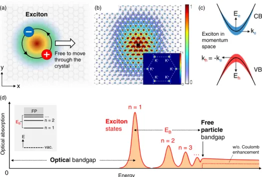
ke Ee
kh= -ke
Eh x
y (a)
Exciton
Free to move through the crystal
(c)
CB
VB Exciton in
momentum space
(d)
Energy
Optical absorption
n = 2 n = 1
n = 3
… Free particle bandgap Exciton
states
Optical bandgap
EB (b)
K+ K-
K- K- K+
K+
0
w/o. Coulomb enhancement n = 1
vac.
EB n = 2
… FP
E
FIG. 2. (a) Schematic real-space representation of the electron-hole pair bound in a Wannier-Mott exciton showing the strong spatial correlation of the two constituents. The arrow indicates the center-of-mass wave vector responsible for the motion of the exciton as a whole. (b) A typical exciton wave function calculated for monolayer MoS2. The modulus squared of the electron wave function is plotted in color scale for the hole position fixed at the origin. The inset shows the corresponding wave function in momentum space across the Brillouin zone, including bothKþandK−exciton states. FromQiu, da Jornada, and Louie, 2013. (c) Representation of the exciton in reciprocal space with the contributions of the electron and hole quasiparticles in the conduction (CB) and valence (VB) bands, respectively, shown schematically by the widths of the shaded areas. (d) Schematic illustration of the optical absorption of an ideal 2D semiconductor including the series of bright exciton transitions below the renormalized quasiparticle band gap. In addition, the Coulomb interaction leads to the enhancement of the continuum absorption in the energy range exceedingEB, the exciton binding energy. The inset shows the atomlike energy level scheme of the exciton states, designated by their principal quantum numbern, with the binding energy of the exciton ground state (n¼1) denoted byEB below the free-particle (FP) band gap.
In addition to the formation of excitons, a closely related consequence of the Coulomb interaction is the so-called self- energy contribution to the absolute energies of electron and hole quasiparticles. In a simplified picture, the self-energy is related to the repulsive interaction between identical charges and leads to an overall increase of the quasiparticle band gap of a semiconductor, i.e., the energy necessary to create an unbound electron-hole pair in the continuum, referred to as the
“
free-particle (or quasiparticle) band gap.
”In many semi- conductors, including TMD monolayers, the self-energy contribution and the exciton binding energy are found to be almost equal, but of opposite sign. Thus, the two con- tributions tend to cancel one another out with respect to the absolute energies.
These interactions are of central importance as they determine the nature of the electronic excitations and the resulting properties of the material. To demonstrate the latter, a schematic illustration of the optical absorption in an ideal 2D semiconductor is presented in Fig. 2(d). The changes asso- ciated with the presence of strong Coulomb interactions result in the formation of the exciton resonances below the renor- malized free-particle band gap. Importantly, the so-called
opticalband gap is then defined with respect to the lowest- energy excitonic feature in absorption, i.e., the ground state of the exciton (n
¼1). The optical gap thus differs from the
free- particleband gap, which corresponds to the onset of the continuum of unbound electrons and holes, as previously introduced. The free-particle band gap is thus formally equivalent to the
n¼∞limit of the bound exciton state.
Consequently, samples with different exciton binding ener- gies and free-particle band gaps can have optical band gaps at very similar energies. This can be further illustrated in comparative studies of the absolute energies of exciton resonances for monolayer samples placed in different dielec- tric environments, effectively tuning both the exciton bind- ing energy and the free-particle band gap (Stier, Wilson et al., 2016; Cadiz et al., 2017; Raja et al., 2017). As a final point, the Coulomb interaction leads to a significant enhancement of the continuum absorption, which is pre- dicted to extend many times of
EBinto the band (Shinada and Sugano, 1966; Haug and Koch, 2009).
In comparison to the direct coupling part of the Coulomb interaction, the exchange contribution denotes the Coulomb interaction combined with the Pauli exclusion principle. The latter is a well-known consequence of the fact that both types of quasiparticles (electrons and holes) result from a sea of indistinguishable charged fermions occupying filled bands:
The wave function of the many-electron system with one carrier promoted to the conduction band should be antisym- metrized with respect to permutations of the particles.
Hence, just as for exchange interaction in atoms, the energy of exciton depends on the mutual orientation of electron and hole spins and, as a particular feature of the TMD MLs, on the quasiparticle valley states. In analogy to the direct coupling, the Coulomb-exchange interaction can also be separated into the long-range and the short-range parts. In particular, the long-range exchange interaction is of electrodynamic nature, in close analogy to the exchange interaction between an electron and a positron (Berestetskii and Landau, 1949). It can thus be interpreted as a result of interaction of an exciton with
the induced electromagnetic field in the process of virtual electron-hole recombination (Denisov and Makarov, 1973; Bir and Pikus, 1974; Goupalov, Ivchenko, and Kavokin, 1998):
The bright exciton can be considered as a microscopic dipole which produces an electric field, and the backaction of this field on the exciton is the long-range electron-hole exchange interaction. On a formal level, it corresponds to the decom- position of the Coulomb interaction up to the dipole term and calculation of its matrix element on the antisymmetrized Bloch functions (Andreani, 1995). In TMD monolayers, the long-range exchange part, being much larger than for III-V or II-VI quantum wells, facilitates transitions between individual exciton states excited by the light of different helicity, thus mainly determining the spin-valley relaxation of the excitons;
see Sec. IV . At short range, Pauli exclusion causes the exchange interaction to strongly depend on the spin and valley states of the particles. It thus contributes to the total energies of the many-particle complexes, depending on the spin and valley states of the individual constituents and impacts the separation between optically dark and bright excitons (Qiu, Cao, and Louie, 2015; Echeverry et al., 2016).
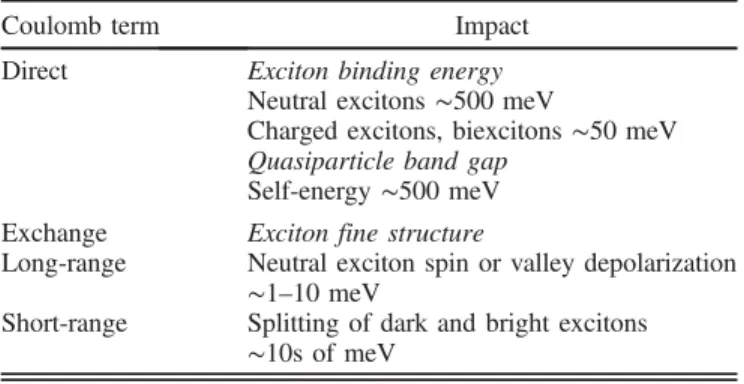
Among typical examples are the so-called triplet and singlet exciton states (i.e., the exciton fine structure) corresponding to parallel and antiparallel alignment of the electron and hole spins, respectively. Lacking a classical analog, the exchange interaction is a more subtle contribution compared to the direct Coulomb interaction. A rough estimate of the exchange to the direct interaction ratio in the exciton is provided by the ratio of the binding energy
EBand the band gap
Eg:
∼EB/E
g(Bir and Pikus, 1974). As summarized in Table I, the overall ratio of the direct and exchange contributions in TMDs is on the order of
10∶1, depending, in particular, on the exciton wave vector for the long-range interaction (Glazov et al., 2014). Nevertheless, as discussed in the following sections, the consequences of the exchange interaction are of central importance in understanding many-particle electronic exci- tations in TMD monolayers.
One of the distinct properties of TMD monolayers is the unusually strong long-range Coulomb interaction and its unconventional interparticle distance dependence, leading to large exciton binding energies and band-gap renormalization effects. First, the decrease of dimensionality results in smaller effective electron and hole separations, particularly, perpendicular to the ML plane, where the wave functions of
TABLE I. The impact of different types of electron-hole interaction on optical and polarization properties of excitons in TMD MLs.
Coulomb term Impact
Direct Exciton binding energy Neutral excitons∼500meV
Charged excitons, biexcitons∼50meV Quasiparticle band gap
Self-energy∼500meV Exchange Exciton fine structure
Long-range Neutral exciton spin or valley depolarization
∼1–10meV
Short-range Splitting of dark and bright excitons
∼10s of meV
the electron and hole occupy only several angstroms as compared to tens of nanometers in bulk semiconductors. In the simple hydrogenic model, this effect yields to a well- known fourfold increase in exciton binding energy in 2D compared to 3D (Ivchenko, 2005). Second, the effective masses in the
Kvalleys of the electron
meand hole
mhin TMD MLs are relatively large, on the order of
∼0.
5m0, with
m0denoting the free electron mass (Liu et al., 2013;
Kormányos et al., 2015). Hence, the reduced mass
μ¼ memh/ðm
eþmhÞ≈0.25m
0is also larger compared to promi- nent semiconductor counterparts such as GaAs (
μ≈0.
06m0).
Finally, in TMD MLs, the material is generally surrounded by air or vacuum (or dielectrics with relatively small permitivity). This reduces dielectric screening of the Coulomb interaction, since the electric field produced by the electron-hole pair is present largely outside of the ML itself. These features of the screening also result in a substantial deviation of the electron-hole interaction from the conventional
1/r distance dependence as discussed in detail in Sec. II.B.2. Nevertheless, one can still estimate the impact of the dimensionality, the effective mass, and the reduced screening on the exciton binding energy
EBwithin the framework of the 2D hydrogenlike model
EB∝4Ry
μ/m
0ε2eff, where Ry is the Rydberg constant of 13.6 eV,
εeffis a typical effective dielectric constant of the system, roughly averaged from the contributions of the ML and the surroundings, and
m0is the free electron mass.
Clearly, an increase in
μand a decrease in
εeffresult in the increase of the binding energy. As an example, this simple expression provides a binding energy compared with other semiconductors on the order of 0.5 eV for realistic param- eters of
μ¼0.
25m0and
εeff ¼5.
As a final step in introducing the Coulomb terms and their role in the physics of TMD monolayers, we can formally identify the direct and exchange terms in the effective exciton Hamiltonian in
kspace in the two-band approximation:
HXX0ðke;kh;k0e;k0hÞ
¼ ½HeðkeÞδke;k0eþHhðkhÞδkh;k0hþVkekh;k0e;k0
hδXX0
þUkekh;k0e;k0
hðEH;E0H0ÞδK;K0; ð2Þ
where
HeðkeÞ[
HhðkhÞ] are the electron (hole) single-particleHamiltonians,
Vkekh;k0e;k0h
stands for the matrix element of the direct (long-range) Coulomb interaction between the electron and the hole, and
Ukekh;k0e;k0hðEH;E0H0Þ
is the matrix of the electron-hole exchange interaction. Here
E¼seτe,
H¼shτhare the electron and hole spin and valley indices, and the dependence of the single-particle Hamiltonians on
Eand
His implicitly assumed. The last term comprises the short- and long-range contributions to the electron-hole exchange inter- action. In real space, the second line of Eq. (2) corresponds to the standard exciton Hamiltonian in the effective mass approximation with a properly screened Coulomb interaction potential with the additional short-range part in the form
V0ðEH;E0H0Þδðre−rhÞand the parameters determined by a particular form of the Bloch functions (Bir and Pikus, 1974).
B. Exciton binding energy
1. Exciton and continuum states in optics and transport
To determine the exciton binding energy
EBdirectly by experiment, one must identify the absolute energy position of both the exciton resonance
EXand that of the free-particle band gap
Egto obtain
EB¼Eg−EX. For this purpose, several distinct techniques have been successfully applied to TMD monolayers. The transition energy
Eðn¼1ÞXof the exciton ground state can be readily obtained using optical methods. Because of the strong light-matter coupling (cf. Sec. II.C) the excitons appear as pronounced resonances centered at photon energies corresponding to
Eðn¼1ÞXin optical absorption, reflectance, PL, photoluminescence excitation (PLE), and photocurrent (PC) measurements. In the case of PL, room-temperature measurements are usually preferred to avoid potential contributions from defect states. As an example, PL spectra of the MoSe
2monolayer are presented in the left panel of Fig. 3(a), illustrating the strong emission from the ground-state exciton transition.
In contrast, the precise determination of the free-particle band-gap energy
Egis a more challenging problem and a recurring one for semiconductors with large exciton binding energies where strong exciton resonances may mask the onset of a continuum of states. A direct approach is provided by the scanning tunneling spectroscopy (STS), which measures tun- neling currents as a function of the bias voltage through a tip positioned in close proximity to the sample. Such measure- ments can probe the electronic density of states in the vicinity of the band gap, mapping energy levels of free electrons in both the valence and conduction bands. A typical STS spectrum for a MoSe
2monolayer supported by a bilayer of graphene (Ugeda et al., 2014) is presented in the right panel of Fig. 3(a). As a function of tip voltage relative to the sample, a region of negligible tunneling current is observed. This arises from the band gap where no electronic states are accessible. The lower and upper onsets of the tunnel current correspond to the highest occupied electron states at the VBM and the lowest unoccupied states at the CBM, respectively. The size of the band gap
Egis extracted from the difference between these onsets. As pre- viously discussed, the exciton binding energy is then directly obtained from the difference between
Egmeasured by STS and the exciton transition energy
Eðn¼1ÞXidentified in the optical spectroscopy [compare right and left panels in Fig. 3(a)].
The reported values, as summarized in Table II, range from 0.22 eV for MoS
2(C. Zhang et al., 2014) to 0.55 eV for MoSe
2(Ugeda et al., 2014); further reports include Bradley et al.
(2015), Chiu et al. (2015), C. Zhang et al. (2015), and Rigosi
et al. (2016). The differences can be related to (i) the overall
precision in extracting the onsets of the tunneling current
and (ii) the use of different conducting substrates required for
STS, i.e., the influence of different dielectric environments
and related proximity effects. In addition, the complexities of
the band structure of the TMDs with several valley extrema
being relatively close in energy (see Sec. I.A) were shown to be
of particular importance for the identification of the bands
contributing to the initial rise in the tunneling current (C. Zhang
et al., 2015).
As discussed in Sec. II.A [see Fig. 2(d)], the onset of the free-particle continuum in the absorption spectra is merged with the series of excited exciton states (n
¼2;3;…), precluding a direct extraction of the band-gap energy in most optical spectroscopy experiments. However, the identification of the series of excited exciton states permits an extrapolation to the expected band gap or for the determination of the band gap through the application of suitable models. These methods are analogous to the measurements of the Rydberg (binding) energy of the hydrogen atom from spectral lines from transitions between different electron states. For an ideal 2D system the exciton energies evolve as
EnB¼ μe4/½2
ℏ2ε2effðn−1/2Þ
2in a hydrogenic series with
n¼ 1;2;…(Shinada and Sugano, 1966; Klingshirn, 2007). As shown in reflection spectroscopy (Chernikov et al., 2014; He et al., 2014), the exciton states in ML WSe
2and WS
2, for example, deviate from this simple dependence; see Fig. 3(b).
The main reason for the change in the spectrum is the nonlocal dielectric screening associated with the inhomogeneous dielectric environment of the TMD ML. This results in a screened Coulomb potential (Rytova, 1967; Keldysh, 1979;
Cudazzo, Tokatly, and Rubio, 2011) with a distance depend- ence that deviates strongly from the usual
1/r form as detailed later and also introduced in the context of carbon nanotubes
(Wang et al., 2005; Adamyan, Smyrnov, and Tishchenko, 2008; Deslippe et al., 2009; Ando, 2010).
The energies of the excited states of the excitons
n >1can be directly obtained from linear absorption or reflectance spectroscopy. These states are usually identified by their decreasing spectral weight (oscillator strength) and relative energy separations with increasing photon energies. The oscillator strength for an ideal 2D system is given by
fn¼ fn¼1/ð2n
−1Þ
3(Shinada and Sugano, 1966). As an example, consider the reflectance contrast spectrum (i.e., the difference of the reflectivity of the sample and substrate divided by the substrate reflectivity) from a WS
2monolayer (Chernikov et al., 2014) measured at cryogenic temperatures. The spectrum, presented after taking a derivative with respect to photon energy to highlight the features in the left panel of Fig. 3(b), reveals signatures of the excited exciton states. The right panel summarizes the extracted peak energies and the estimated position of the band gap, as obtained directly from the extrapolation of the data and from model calculations. The corresponding exciton binding energy is about 300 meV.
Observations of the excited states in reflectance spectra were further reported for WSe
2(He et al., 2014; Arora, Koperski et al., 2015; Hanbicki et al., 2015) and WS
2(Hanbicki et al., 2015; Hill et al., 2015) monolayers, both at cryogenic and
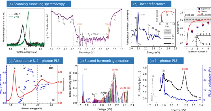
(a) (b)
(c) (d) (e)
FIG. 3. Presentation of commonly used experimental techniques to determine exciton binding energies in TMD monolayers.
(a) Direct measurement of the free-particle band-gap energy using scanning tunneling spectroscopy of ML MoSe2 on bilayer graphene (right panel) combined with a measurement of the absolute energy of the exciton ground state from photoluminescence (left panel). From Ugeda et al., 2014. (b) Exciton states of ML WS2 on a SiO2/Si substrate from reflectance contrast measurements. The extracted transition energies of the states and the inferred band-gap position are presented in the right panel.
From Chernikov et al., 2014. (c) The linear absorption spectrum and the third-order susceptibility extracted from two-photon photoluminescence excitation spectra of ML WSe2 on fused silica substrate with exciton resonances of the ground and excited states. FromHeet al., 2014. (d) Exciton states as measured by second-harmonic spectroscopy of theAandBtransitions in ML WSe2. From Wang, Marie, Gerber et al., 2015. (e) One-photon photoluminescence excitation spectra and the degree of linear polarization of the luminescence of ML WSe2with features of the excited2sstate of theAand the ground state of theBexciton.
From Wang, Marie, Gerber et al., 2015.
room temperature, as well as for MoSe
2(Arora, Nogajewski et al., 2015). In addition, the relative energy separations between the ground and excited states of the excitons were found to decrease with the thickness of multilayer samples (Chernikov et al., 2014; Arora, Koperski et al., 2015), reflecting the expected decrease in the binding energy.
Similar results were obtained by the related techniques of PLE (Hill et al., 2015; Wang, Marie, Gerber et al., 2015) and PC (Klots et al., 2014) spectroscopy, which also allow identification of the ground and excited-state excitonic tran- sitions. In both cases, this is achieved by tuning the photon energy of the excitation light source, while the luminescence intensity of a lower-lying emission feature (in PLE) or the current from a sample fabricated into a contacted device (in PC) are recorded. PLE is a multistep process: light is first absorbed, then energy relaxation occurs to the optically active
1sexciton. As relaxation via phonons plays an important role in TMD MLs (Molina-Sánchez and Wirtz, 2011; Chow et al., 2017), the PLE spectra contain information on both absorption and relaxation pathways. From PLE measurements, excited states of the excitons were observed in WSe
2(Wang, Marie, Gerber et al., 2015), WS
2(Hill et al., 2015), MoSe
2(Wang, Gerber et al., 2015), and MoS
2(Hill et al., 2015) monolayers.
In PC, the onset of the band-gap absorption in MoS
2monolayers was reported by Klots et al. (2014).
One of the challenges for linear absorption or reflectance spectroscopy is the dominant response from the exciton ground state, potentially obscuring weaker signatures from the excited states. As an alternative, excited states of the excitons, for example,
ðn;1Þ ¼ ðnp;1Þfor
n >1can be addressed via two-photon excitation in TMDs (Ye et al., 2014; Berkelbach, Hybertsen, and Reichman, 2015;
Srivastava and Imamoglu, 2015; Wang, Marie, Gerber et al., 2015), while the two-photon absorption by the dipole- allowed transitions for
ðn;0Þ ¼1s;2s;3s;…is suppressed.
Indeed, in the commonly used centrosymmetric model
s-shell excitons are allowed in one-photon processes (andforbidden in all processes involving an even number of phonons), while
p-shell excitons are allowed in two-photonprocesses and forbidden in one-photon processes (Mahan, 1968). Note that the specific symmetry of the TMD ML can lead to a mixing between exciton
sand
pstates and activation of
pstates in single-photon transitions as well (Glazov et al., 2017; Gong et al., 2017). The mixing is also proposed to originate from a small amount of disorder in the system (Berghäuser, Knorr, and Malic, 2016).
Here a commonly used technique is two-photon photo- luminescence excitation spectroscopy (2P-PLE). In this method, the (pulsed) excitation source is tuned across the range of half the
pexciton transition energy and the resulting luminescence is recorded as a function of the photon exci- tation energy. Formally, this yields the spectrum of third-order nonlinear susceptibility responsible for two-photon absorp- tion. The result of such a 2P-PLE measurement of a WSe
2monolayer (He et al., 2014) is presented in Fig. 3(c). In contrast to one-photon absorption, the two-photon response is dominated by resonances from the excited exciton states with
p-type symmetry, such as the 2p; 3p;…states of the
Aexciton [labeled
A00in Fig. 3(c)]. Further reports of the exciton states in 2D TMDs from 2P-PLE include studies of WS
2(Ye et al., 2014; Zhu, Chen, and Cui, 2015), WSe
2(Wang, Marie, Gerber et al., 2015), and MoSe
2monolayers (Wang, Gerber et al., 2015). Similar to the analysis of the one- photon spectra, the band gap is extracted either by comparison of the ground- and excited-state energies with appropriate theoretical models (Ye et al., 2014; Wang, Marie, Gerber et al., 2015) or from the estimated onset of the continuum absorption (free-particle gap) (He et al., 2014; Zhu, Chen, and Cui, 2015). In addition to the PLE experiments, both the ground and excited states can also be observed directly in second-harmonic generation spectra, as illustrated in Fig. 3(d) for WSe
2monolayers (Wang, Marie, Gerber et al., 2015). The second-harmonic generation takes place because, due to the lack of an inversion center in TMD MLs, the
s-shell and p-shell excitons become active in both one- and two-photon processes. This allows for excitation of the given exciton state by two photons and its coherent emission. The microscopic analysis of the selection rules and relative contributions of excitonic states in second-harmonic emission is presented by Glazov et al. (2017); see also Trolle, Seifert, and Pedersen (2014). Overall, the main challenge with optical techniques is the correct identification of observed features, made more challenging by the possible mixture of
sand
pexcitons, as well as coupling to phonon modes (Chow et al., 2017; Jin et al., 2017). Topics of current discussion in analyzing different spectra include possible contributions from pho- non-assisted absorption, higher-lying states in the band structure, defects, and interference effects.
Further information on exciton states and their energy can be obtained from measurements of intraexciton transitions in the mid-IR spectral range after optical injection of finite exciton densities (Poellmann et al., 2015; Cha et al., 2016) and measurements of the exciton Bohr radii from diamagnetic shifts at high magnetic fields (Stier, McCreary et al., 2016;
Stier, Wilson et al., 2016). The latter approach also allows for the estimation of the binding energy of the
Bexciton related to the spin-orbit split valence subband. A summary of the exciton binding energies and the corresponding band-gap energies is presented in Table II. While the extracted absolute values vary, largely due to the outlined challenges of precisely determining the absolute position of the band gap, the following obser- vations are compatible with the majority of the literature.
(1) Excitons are tightly bound in TMD monolayers due to the quantum confinement and low dielectric screening with binding energies on the order of several hundred of meV.
The corresponding ground-state Bohr radii are on the order of nanometers and the wave function extends over several lattice constants
a0(e.g., for WSe
2 a0≈0.
33nm), rendering the Wannier-Mott exciton model largely applicable.
(2) The absolute position of the free-particle band gap renormalizes by an amount similar to the exciton binding energy in comparison to the respective
K−Ktransition in bulk. Thus, only a modest absolute shift of the exciton energy is observed in optical spectra when comparing the bulk and monolayers.
(3) The Coulomb interaction deviates from the
1/r law due
to the spatially inhomogeneous dielectric screening environ-
ment (see Sec. II.B.2). This changed distance dependence of
the
e−hinteraction strongly affects the energy spacing of the
n¼1;2;3;…
exciton states leading to pronounced deviations from the 2D hydrogen model.
2. Effective Coulomb potential and the role of the environment
Calculations of excitonic states and binding energies in TMD MLs have been performed by many approaches, including effective mass methods, atomistic tight-binding, and density functional theory with various levels of sophistication (Cheiwchanchamnangij and Lambrecht, 2012; Komsa and Krasheninnikov, 2012; Ramasubramaniam, 2012; Molina- Sánchez et al., 2013; Qiu, da Jornada, and Louie, 2013; Shi, Pan et al., 2013; Berghäuser and Malic, 2014; Molina-Sánchez, Hummer, and Wirtz, 2015; Stroucken and Koch, 2015; Wu, Qu, and MacDonald, 2015; Trushin, Goerbig, and Belzig, 2016;
Gillen and Maultzsch, 2017). A simple and illustrative approach to calculate energies of exciton states is provided by the effective mass method. Here in the Hamiltonian (2) the single-particle kinetic energies
HeðkeÞand
HhðkhÞare replaced by the operators
−ðℏ2/2m
eÞ∂2/
∂ρ2eand
−ðℏ2/2m
hÞ∂2/
∂ρ2h, respectively, with
ρeand
ρhbeing the electron and hole in- plane position vectors. Most importantly, the electric field between individual charges in the ML permeates both the material layer and the surroundings outside the monolayer. As a consequence, both the strength and the form of the effective Coulomb interaction between the electron and hole in the exciton are strongly modified by the dielectric properties of the environment (Rösner et al., 2016; Stier, Wilson et al., 2016;
Raja et al., 2017). In principle, one recovers a 2D hydrogenlike
problem with an adjusted effective potential by taking into account the geometry of the system and the dielectric surround- ings (Rytova, 1967; Keldysh, 1979; Cudazzo, Tokatly, and Rubio, 2011; Berkelbach, Hybertsen, and Reichman, 2013;
Chernikov et al., 2014; Ganchev et al., 2015).
Typically, the combined system
“vacuum + TMD monolayer + substrate
”is considered, reproducing the main features of the most common experimentally studied samples. In the effective medium approximation, the dielectric constant
ε∼10of the TMD ML generally far exceeds the dielectric constants of the surroundings, i.e., of the substrate
εsand of the vacuum. As a result, the effective interaction potential takes the form of
∝1/
ρ(
ρ¼ρe−ρhis the relative electron-hole coordinate) only at large distances between the particles where the electrical field resides outside the TMD ML itself. At smaller distances, the dependence is
∝logð
ρÞ(Cudazzo, Tokatly, and Rubio, 2011).
The resulting overall form of the effective potential, following Rytova (1967) and Keldysh (1979), is given by
VðρÞ ¼− πe2 ð1þεsÞr0
H0
ρ r0
−Y0 ρ
r0
; ð3Þ
where
H0ðxÞand
Y0ðxÞare the Struve and Neumann functions, and
r0is the effective screening length. The latter can be either calculated from
ab intio(Berkelbach, Hybertsen, and Reichman, 2013) or considered as a phenomenological parameter of the theory (Chernikov et al., 2014) and typically ranges from roughly 30 to 80 Å. Then within the effective mass approximation, the two-particle Schrödinger equation with the effective potential
VðρÞin the form of Eq. (3) can be
TABLE II. Summary of experimentally determined exciton binding energies and free-particle band gaps in monolayer TMDs from the literature. All values correspond to theA-exciton transition, unless noted otherwise. The numerical formats correspond to the presentations of the data in the respective reports. Abbreviated are room temperature (RT), highly ordered pyrolytic graphene (HOPG), molecular beam epitaxy (MBE), and second-harmonic generation (SHG); in addition,“Refl.”and“Exf.”indicate“reflectance”and“exfoliated,”respectively.Material
Sample (temperature)
Experimental technique
Binding energy (eV)
Band
gap (eV) Reference
WSe2 Exf. on SiO2/Si (RT) Refl., 2P-PLE 0.37 2.02 Heet al.(2014)
CVD on HOPG (79 K) STS, PL 0.5 2.20.1 C. Zhanget al.(2015a)
Exf. on SiO2/Si (4 K) PLE, 2P-PLE, SHG 0.60.2 2.350.2 Wang, Marie, Gerberet al.(2015)
Exf. on SiO2/Si (4–300 K) Refl. 0.887 2.63 Hanbickiet al.(2015)
CVD on HOPG (77 K) STS, PL ≈0.4a 2.080.1 Chiuet al.(2015)
Exf. on diamond (RT) Mid-IR pump probe 0.245 1.9b Poellmannet al.(2015) WS2 Exf. on SiO2/Si (5 K) Refl. 0.320.04 2.410.04 Chernikovet al.(2014)
Exf. on fused silica (10 K) 2P-PLE 0.7 2.7 Yeet al.(2014)
Exf. on SiO2/Si (RT) 2P-PLE 0.710.01 2.73 B. Zhuet al.(2014)
Exf. on SiO2/Si (4–300 K) Refl. 0.929 3.01 Hanbickiet al.(2015)
Exf. on fused silica (RT) Refl., PLE 0.320.05 2.330.05 Hillet al.(2015) Exf. on fused silica (RT) STS, Refl. 0.360.06 2.380.06 Rigosiet al.(2016)
CVD on SiO2(4 K) Magnetoreflection 0.26–0.48 2.31–2.53b Stier, McCrearyet al.(2016) MoSe2 MBE on2L
graphene/SiC (5 K)
STS, PL 0.55 2.18 Ugedaet al.(2014)
CVD on HOPG (79 K) STS, PL 0.5 2.150.06 C. Zhanget al.(2015a)
MoS2 CVD on HOPG (77 K) STS, PL 0.2 (or 0.42) 2.150.06 C. Zhanget al.(2014)
Exf., suspended (77 K) PC ≥0.57 2.5 Klotset al.(2014)
Exf. on hBN/fused silica (RT) PLE 0.440.08c 2.470.08c Hillet al.(2015)
CVD on HOPG (77 K) STS, PL ≈0.3a 2.150.1 Chiuet al.(2015)
Exf. on fused silica (RT) STS, Refl. 0.310.04 2.170.1 Rigosiet al.(2016)
aExtracted from the PL data and STS results inChiuet al.(2015).
bObtained by adding the estimated exciton binding energies to the resonance energy inPoellmannet al.(2015)andStier, McCreary et al., 2016.
cAttributed to theB-exciton transition byHillet al.(2015).