Controlled thermodynamics for tunable electron doping of graphene on Ir(111)
C. Struzzi,1,2C. S. Praveen,3M. Scardamaglia,2N. I. Verbitskiy,4,5A. V. Fedorov,6,7,8M. Weinl,9M. Schreck,9A. Gr¨uneis,6 S. Piccinin,3S. Fabris,3,*and L. Petaccia1,†
1Elettra Sincrotrone Trieste, Strada Statale 14 km 163.5, 34149 Trieste, Italy
2Chimie des Interactions Plasma Surface (ChIPS), University of Mons, 7000 Mons, Belgium
3Consiglio Nazionale delle Ricerche (CNR)–Istituto Officina dei Materiali (IOM) DEMOCRITOS, and Scuola Internazionale di Studi Superiori Avanzati (SISSA), Via Bonomea 265, I-34136, Trieste, Italy
4Faculty of Physics, University of Vienna, Strudlhofgasse 4, A-1090 Vienna, Austria
5Department of Materials Science, Moscow State University, Leniskie Gory 1/3, 119991 Moscow, Russia
6II Physikalisches Institut, Universit¨at zu K¨oln, Z¨ulpicher Strasse 77, 50937 K¨oln, Germany
7Institute for Solid State Research, IFW Dresden, P.O. Box 270116, D-01171 Dresden, Germany
8St. Petersburg State University, St. Petersburg 198504, Russia
9Institut f¨ur Physik, Universit¨at Augsburg, D-86135 Augsburg, Germany
(Received 1 April 2016; revised manuscript received 18 July 2016; published 25 August 2016) The electronic properties and surface structures of K-doped graphene supported on Ir(111) are characterized as a function of temperature and coverage by combining low-energy electron diffraction, angle-resolved photoemission spectroscopy, and density functional theory (DFT) calculations. Deposition of K on graphene at room temperature (RT) yields a stable (√
3×√
3)R30°surface structure having an intrinsic electron doping that shifts the graphene Dirac point byED=1.30 eV below the Fermi level. Keeping the graphene substrate at 80 K during deposition generates instead a (2×2) phase, which is stable until full monolayer coverage. Further deposition of K followed by RT annealing develops a double-layer K-doped graphene that effectively doubles the K coverage and the related charge transfer, as well as maximizing the doping level (ED=1.61 eV). The measured electron doping and the surface reconstructions are rationalized by DFT calculations. These indicate a large thermodynamic driving force for K intercalation below the graphene layer. The electron doping and Dirac point shifts calculated for the different structures are in agreement with the experimental measurements.
In particular, the K4sbands are shown to be sensitive to both the K intercalation and periodicity and are therefore suggested as a fingerprint for the location and ordering of the K dopants.
DOI:10.1103/PhysRevB.94.085427 I. INTRODUCTION
Exploiting the exceptional properties of graphene requires engineering its characteristic zero-gap semimetal electronic structure [1]. In particular, ever-increasing experimental efforts aim at tuning its optical and electronic properties in order to open a band gap, which underpins the development of devices based on novel nanoarchitectures [2–5]. The electronic properties of graphene can be tuned by a controlled surface decoration with adatoms, heteroatoms [6–8], or molecules [9,10]. Alkali metal atoms represent very flexible systems for n-type doping graphene [11]. The appealing electronic structure obtained by alkali doping has already been studied for different carbon nanomaterials such as fibers [12], carbon nanotubes [13–17], graphite [18–20], and graphene [11,21–26]. Since the chemical bonding between the C and alkali atoms is dominated by the electrostatics resulting from charge transfer effects, a rigid-band model is widely employed for doped C materials [19,27–30]. Within this model, the doping purely results in a Fermi level shift, i.e., in a band structure offset. In particular, forn-doping the C-related electronic band structure experiences a downshift to higher binding energies (BEs). This opens the possibility of exploring the region of the graphene band structure above the
*Corresponding author: fabris@democritos.it
†Corresponding author: luca.petaccia@elettra.eu
Dirac point by angle-resolved photoemission spectroscopy (ARPES) [19,24,25,31,32]. The partial ionization of alkali metals generates vertical dipoles, and their mutual repulsion contribute to the formation of regular patterns [20], which are observed, for instance, by low-energy electron diffraction (LEED) technique. The most commonly observed stoi- chiometries obtained by depositing alkali-metal (M) atoms on graphitic surfaces areMC6andMC8(depending onM), which are related to the (√
3×√
3)R30°(√ 3×√
3 in the following) and (2×2) reconstructions with respect to the carbon (1×1) lattice, respectively [21,24,25,27,28,30,32–35]. The formation of these regular patterns often emerges after overcoming a critical amount of alkali deposition on the surface. Potassium adsorbed on graphite suitably represents a case study in which the initial dispersed K phase, forming at low coverages (<0.1 monolayer [ML]), is continuously compressed as a function of adatom density until reaching a critical coverage (0.1–0.3 ML) that defines the coexistence of dispersed and close-packed (2×2) phases. The (2×2) configuration holds until an entire covering of the surface is obtained, which defines 1 ML coverage [27,28,36,37]. Additional depositions result in disordered films [27,28,36,37], corresponding to multilayered coverages that in some cases were observed to form structures with (√
3×√
3) periodicity as a consequence of contaminants such as oxygen on the graphitic surface [28,31,38].
In the specific case of potassium deposition on graphene, previous works reported on the adsorbed (2×2) periodicity, showing that a band structure with the Dirac cone downshifted
at higher BE and the partially filled potassium K4s states centered at the point of the Brillouin zone (BZ). This K4s band is instead upshifted above the Fermi level when potassium is intercalated [21,22,39]. The charge carrier density related to the charge transfer from the alkali metal to graphene is proportional to the material’s Fermi surface area [40]. In the rigid-band model, this and the corresponding doping level, i.e., the number of extra electrons (e) per C atom, can be directly related to the energy shift of the Dirac point (ED) with respect to the Fermi level (EF) [27,28]. Both the electron doping and the charge transfer depend crucially on the adatom configurations and on the position of the alkali layer with respect to the carbon one: for example, Pan et al. reported the variation ofEDfrom 1.35 eV to 0.82 eV for KC8or LiC6, respectively [34]. Furthermore, the charge carrier densities and the values ofEDwere reported to depend on the specific alkali dopant (KC8,CsC8,RbC8,NaC8,LiC6,CaC6), and it was suggested that for quasi-free-standing supported graphene, the location of the dopant with respect to the interface (on top of graphene or at the substrate/graphene interface) influences largely the interlayer state’s wave function [11,23,41].
In the present paper, we measure the electronic and struc- tural properties of potassium-doped graphene on iridium films, K-Gr/Ir(111), by ARPES and LEED. The electronic band structure evolution of Gr/Ir(111) under subsequent potassium deposition is presented at different substrate temperatures, i.e., room temperature (RT), T =80 K, and after heating up to T =360 K. The observed (√
3×√
3) and/or (2×2) LEED patterns are described in detail for each system in combination with photoemission spectra to correlate the periodicity to its respective doping level. We perform density functional theory (DFT) calculations to investigate the preferred location of alkali metal atoms with respect to the graphene sheet through a detailed thermodynamic analysis. We consider several geo- metric arrangements of the dopants on the graphene surface, differing in the periodicity and in the position with respect to the graphene layer, and we discuss their effect on the band structure of graphene and on the charge transfer. We conclude by exploring the experimental realization of double-side alkali doped graphene with both adsorbed and intercalated K. In this K-doped graphene sandwich architecture, the maximal doping is reached with ED =1.61 eV and with a massive charge transfer that almost doubles the value of single-side doped graphene, as confirmed by the theoretical results.
II. METHODS A. Experimental
Chemical vapor deposition (CVD) was used for graphene growth on iridium films Gr/Ir(111). The procedure details and the characterization of monolayer quality are reported in a previous paper [42]. Potassium was evaporated in situfrom a well-degassed commercial SAES Getters dispenser keeping the pressure in the 10−10mbar range in the ultra-high vacuum (UHV) preparation chamber, directly connected to the analysis chamber. Since the temperature (T) is a key parameter to realize adsorption or intercalation of potassium atoms on the carbon lattice [27], the sample was kept at RT or atT =80 K while ex- posing the surface to subsequent potassium evaporation steps
(duration of 5 minutes each, unless otherwise specified) start- ing from low coverages, upon reaching saturation, and over- coming monolayer coverage. We refer saturation to the stage at which no further shift of the Dirac cone is observed by ARPES and a clear reconstruction emerges in LEED. For the RT exper- iment, no annealing treatments were needed either to facilitate or to improve the intercalation process. In the low temperature case, the intercalation was instead achieved after a RT stage of 15 minutes following the last alkali deposition atT =80 K.
In both cases, potassium intercalates mainly through graphene step edges and grain boundaries as the graphene layer is ho- mogeneous and almost defect-free, as shown by our previous scanning tunneling microscopy (STM) study [42].The ARPES and LEED measurements were carried out at the BaDElPh beamline of the Elettra synchrotron in Trieste [43]. Using both horizontal (p) and vertical (s) polarized radiation and a photon energy of 34 eV, we followed the dispersion ofπandσ states of graphene in the valence band by scanning the BZ along the KandM high symmetry directions and got access to the details of the regions of particular interest. The overall energy and angular resolutions were better than 50 meV and 0.3°, respectively. The Fermi surface was acquired by scanning the azimuthal angle of about 50°around the Kpoint of the BZ with steps of 0.5°. The energy position of the Dirac point was obtained by fitting the momentum distribution curves (MDCs) of the ARPES images with Lorentzian line shape peaks and then applying, around the Dirac point, the linear regression analysis by using maximum-minimum slope best-fit lines to determine the final uncertainty in the stated value. The LEED patterns of potassium doped graphene on iridium films were collected by setting the electron beam energy atE=75 eV and an incidence angle of 0°from the sample surface normal.
B. DFT calculations
All the DFT calculations presented in this paper employed the Perdew-Burke-Ernzerhof (PBE) exchange and correlation functional [44] and were performed using the PWscf code of the Quantum ESPRESSO package [45]. The Kohn-Sham equations were solved in periodic boundary conditions, de- scribing the electron-ion interaction with ultrasoft Vanderbilt pseudopotentials [46], and representing the valence electron wave function with a plane-waves basis set limited by a kinetic energy cutoff of 35 Ry (350 Ry for the charge density). All the calculations presented here are nonspin polarized since none of the systems under analysis has unpaired electrons.
The long-range van der Waals (vdW) forces were explicitly included in the calculations by adding to the PBE functional the Grimme’s semiempirical correction term (DFT-D2) [47].
The role of this correction on the electronic and structural properties of metal-supported graphene has been analyzed in a previous work [48]. Integrals in the BZ were calculated on a 14×14×1 (12×12×1) Monkhorst-Pack k-point grid for the 2×2 (√
3×√
3) cell, using a Gaussian smearing of 0.01 Ry. On larger unit cells, the k-point grid was rescaled accordingly. To visualize the atom projected band structure, we used the technique of resolving the projected density of states in the k-space, where the Kohn-Sham states, at every k-point, are projected on atomic states. For this purpose we performed nonself-consistent calculations using 39 (41)
symmetry nonequivalent k-points along the-K-M-(M- K--K) direction of the irreducible part of the BZ for the 2×2 (√
3×√ 3) cell.
Concerning the substrate modeling, capturing the ∼10%
mismatch between the graphene and Ir(111) lattice parameters would require larger Gr(10 × 10)/Ir(9 ×9) computational supercells. With respect to the 2×2 and (√
3×√ 3) cells, the Gr(10 × 10)/Ir(9 × 9) model would certainly provide a better description of the interlayer distance modulation as well as of the C-Ir interaction [49]. However, the dispersion of the electron states calculated in these supercells would be multiply folded in the corresponding primitive BZ and would make the comparison with ARPES measurement quite complicated. The postprocessing required to unfold the bands into the standard graphene BZ is known to be expensive and technically difficult [50]. To allow for a clearer comparison between the calculated band structure and the ARPES spectra, the Gr/Ir(111) system was simplified and was modeled with the 2×2 and (√
3×√
3) cells as a commensurate interface.
Following previous works [32,39,51], we fixed the lattice constant of bulk face-centered-cubic (fcc) Ir as 3.5 ˚A (i.e., Ir is compressed by about 8%), resulting in a lattice constant of 2.47 ˚A for both the Ir(111) surface and the graphene layer. The Gr/Ir(111) system was modeled with supercell slabs having lateral periodicities ranging from (√
3×√ 3) to (4×4) and, along the direction perpendicular to the surface, comprising four Ir atomic layers, one graphene layer, and more than 15 ˚A of vacuum. The symmetry-inequivalent carbon atoms of the graphene overlayer were placed above the top and hexagonal-close-packed (hcp) sites, respectively, of the Ir(111) surface. To model K-doped graphene, we placed a K atom above and/or below the center of a hexagonal carbon ring. Coverage effects were explored by considering mainly the (√
3×√
3) and (2×2) cases, but also the (2√ 3×2√
3) and (4×4) periodicities were considered, as reported in the Supplemental Material [55]. A representative model used in the present paper is displayed in Fig.1. Following previous works [52], the atomic coordinates of the graphene and K layers were relaxed, while the Ir atoms were fixed to their bulk lattice sites. Note that fixing the Ir atoms to their bulk sites has negligible effects on the electronic properties [32,51].
All the adsorption/intercalation energies (Eb) are calculated using the following energy difference,
Eb=ETotal−(E(Gr/Ir)+NKEK),
where ETotal andE(Gr/Ir) represent the total energies of the Gr/Ir system with and without potassium intercalated and/or adsorbed, whileNKandEKrepresent the number of K atoms and the total energy of a K atom in the gas phase, respectively.
The Gibbs’s free energy of adsorption/intercalation was calculated usingab initioatomistic thermodynamics [53]. The thermodynamic stability of different periodicities of potassium is obtained by assuming the system to be in equilibrium with a reservoir of K atoms in gas phase. The free energyG(ads) of K adsorbed and/or intercalated at the Gr/Ir(111) substrate can be written as (see the Supplemental Material [55] for more details),
G(ads)= Eb
S − NK
S μK(T ,p)
,
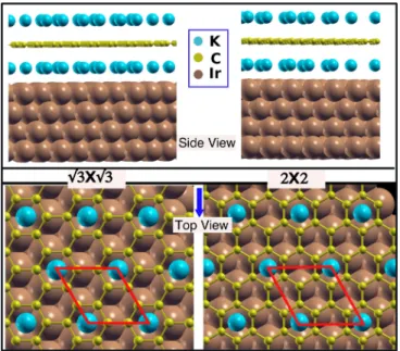
FIG. 1. Top and side views of the structural model used in the calculations to represent K adsorption/intercalation at the Gr/Ir(111) interface. Ir, C, and K atoms are represented by brown, yellow, and blue spheres, respectively. The (√
3×√
3) and (2×2) unit cells are marked by the red lines.
whereSis the surface area andμKis the chemical potential of potassium. The temperature and pressure dependence of μKis assumed to be that of an ideal gas.
III. RESULTS AND DISCUSSION A. Potassium intercalation
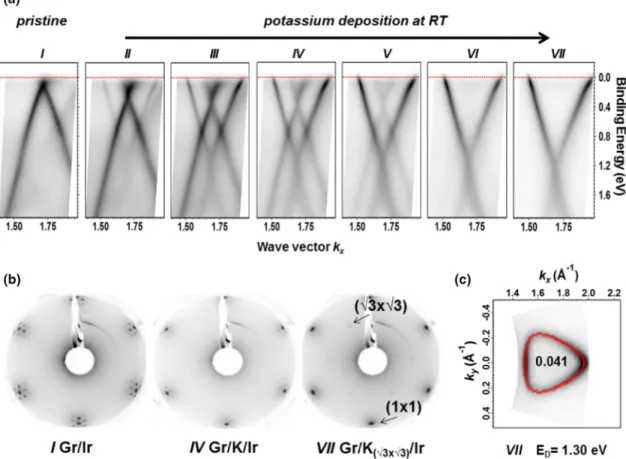
We have initially followed the behavior of potassium deposited by steps on the sample kept at RT since intercalation is known to be favored for graphene and graphite under these conditions [5,25,32,36,37]. The ARPES images reported in Fig.2(a)display the evolution of the Dirac cone, centered at theKpoint of the BZ (wave vector 1.7 ˚A−1), from the pristine Gr/Ir(111) (I) and upon subsequent potassium depositions (II- VII). The two branches of the cone are disclosed by summing the photoemission data acquired in p and s polarization in order to identify the energy position of the Dirac point, which is roughly located at the Fermi level for the pristine sample [42].
Already after the first alkali metal depositions, the Dirac cone downshifts to higher BEs due to the charge transfer from K to C atoms. Differently doped Dirac cones are visible in the data [see Fig.2(a), II-VI], whose relative intensities change after each evaporation step, similar to the recent results reported for cesium doped graphene [25]. These intermediate multiple phases correspond to an inhomogeneous intercalation that ends up in a uniformly intercalated potassium layer when a single n-doped Dirac cone is observed [Fig. 2(a), VII]. Further K evaporation steps do not shift the Dirac energy anymore but weaken the cone intensity.
In Fig.2(b), the measured LEED patterns are displayed for pristine graphene on iridium (left), showing the well-known moir´e superstructure [42], and for the potassium deposition steps IV (center) and VII (right). The intensity related to
FIG. 2. (a) ARPES images (vertical axis: binding energyE−EFreferenced to the Fermi levelEF; horizontal axis: wave vectorkx) of the Dirac cone alongKMdirection acquired at RT for the pristine sample (I) and after subsequent potassium depositions (II-VII), summing the data forsandppolarization. (b) The LEED images for pristine graphene (left) and for potassium doped graphene at IV (center) and VII (right) step, respectively. (c) Fermi surface map for maximal doping at RT withED=1.30±0.05 eV (case VII). Red points denote ARPES intensity maxima extrapolated from the data to calculate the number of extra electrons per C atom displayed inside the contour.
the initial moir´e superstructure gradually decreases, and a (√
3×√
3) periodicity is discernible only when the saturation is attained, thus suggesting the achievement of potassium intercalation. We refer to this system as Gr/K(√
3×√ 3)/Ir, and, to our knowledge, only the (2×2) phase has been reported so far for K doped graphene [21,22,39,54]. On the contrary, the (√
3×√
3) periodicity was observed for potassium doped graphite in early studies when more than 1 ML coverage was dosed at low temperature [31,38]. Its appearance was justified by the presence of a contaminant, such as oxygen on the graphitic surface, that stabilizes the reconstruction [28,31,38]. Nevertheless this interpretation cannot be validated for our system since we never detected oxygen impurities on the pristine [42] and doped sample (see Fig. S1 and Fig. S2 in the Supplemental Material [55]), and we demonstrate in the present paper the energetic preference for potassium to intercalate at RT in a (√
3×√
3) registry for the Gr/Ir system.
In Fig. 2(c), we report the Fermi surface map acquired after the last alkali deposition step (VII). The number of extra electrons per C atom (n) is calculated from the ratio of the Fermi surface area to the area of the BZ [56,57]. We found n=0.041±0.005e per C atom with a doping inducing a maximal downshift of the Dirac cone ofED =1.30±0.05 eV for the Gr/K(√
3×√
3)/Ir system.
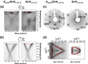
B. Potassium adsorption and double-side configuration Different results are obtained when potassium deposition is performed by keeping the sample atT =80 K. In Fig.3, we report low temperature LEED images (a) and ARPES maps (b) acquired around the K point of the graphene BZ from pristine (I), potassium doped graphene after 10 minutes (II), and 20 minutes (III) of evaporation, and after a subsequent RT treatment (IV). In alkali doped samples, the LEED images show the presence of the moir´e spots also all around the emerg- ing (2×2) reconstruction. No alteration is obtained in the diffraction pattern when the amount of alkali atoms overcomes monolayer coverage except for a diffusive background increase [Fig. 3(a), from case II to III]. A downshifted Dirac cone withED=1.00±0.03 eV is observed in the relative ARPES spectra with essentially a weakening of the cone intensity as a function of deposition [Fig. 3(b), II and III]. These observations suggest that potassium is adsorbed, with a (2×2) periodicity, on top of graphene when deposition is performed atT =80 K, thus resulting in the K(2×2)/Gr/Ir system. The appearance of a dispersed 4s state of potassium (K4s) in ARPES around thepoint (see Fig. S3 in the Supplemental Material [55]), crossing the Fermi level at around±0.45 ˚A−1, further strengthens this picture. In fact, alkali 4s bands appear below the Fermi level when alkali atoms are adsorbed
FIG. 3. (a) LEED and (b) ARPES images atT =80 K are shown for: pristine Gr/Ir (I), potassium adsorbed K(2×2)/Gr/Ir system after 10 min. (II) and 20 min. (III) of evaporation, and after a subsequent RT treatment providing the K/Gr/K/Ir system (IV). The ARPES images are acquired along theKMhigh symmetry direction around theK point.
on graphene, as the partial ionization, due to incomplete depletion, encourages the interaction between adatoms from the neighboring cells, which induces the formation of metallic bonds [19,23,27,31,39].
Once the sample is kept at RT for 15 minutes, the thermal energy increases the mobility by giving the adatoms the possibility to intercalate. The LEED does not display any moir´e in the (2×2) reconstruction, and the diffusive background decreases [see Fig. 3(a) IV]. The ARPES data show the appearance of a well-defined Dirac cone, which is downshifted to the maximal value ofED=1.61±0.04 eV [Fig.3(b), IV].
This is remarkably larger than the usual value of about 1.3 eV reported in literature for the (2×2) phase of potassium- doped graphene [39,54]. A similar ED of about 1.6 eV was recently reported by Pervanet al.for Li doped Gr/Ir(111) [26]
and, previously, by McChesneyet al.for Ca or Ca+K doped graphene on SiC(0001) [58]. We note here that, in agreement with previous works on K doped Gr/Ir [21,22], on Na adsorbed Gr/Ir [24], and on Cs intercalated Gr/Ir [25], we have not found any sign of restoring of the Ir surface state below EF and around theK point as instead recently reported for Gr/(1× 1)Li/Ir(111) [26] and (10×10)Gr/(9×9)Cu/Ir(111) [59]. We speculate that this different behavior may rely on the different packaging of the alkaline metal. The following scenario thus depicts our system when it is kept at T =80 K: At each deposition, potassium atoms do not have enough mobility to intercalate, and they remain on the cold surface of the sample; a charge transfer is initiated from potassium to the carbon atoms, and the repulsion between neighboring alkali ions induces an ordered (2×2) structure on top of the carbon lattice due to emerging vertical dipoles at the surface. Further K evaporation on the sample kept at 80 K does not modify the
FIG. 4. The ARPES measurements acquired atT =80 K around (a)point and (b)Kpoint from potassium-doped graphene sandwich K(2×2)/Gr/K(√
3×√
3)/Ir (left column) and from potassium inter- calated graphene Gr/K(√
3×√
3)/Ir (right column) obtained after subsequent heating atT =360 K. (c) LEED images acquired from the two systems. Together with the (1×1) spots related to Gr/Ir, both reconstructions are visible for the sandwich configuration: a more intense (2×2) superimposed on a (√
3×√
3), while in the intercalated system only the (√
3×√
3) reconstruction is detected.
(d) Corresponding Fermi surface maps. Red points denote ARPES intensity maxima used to calculate the number of extra electrons per C atom displayed inside each Fermi surface plot.
pattern, which is only weakened by an increasing background.
As soon as the K atoms have the possibility to intercalate, thanks to the RT treatment, the LEED superstructure becomes clearly visible with no moir´e spots, and in ARPES,EDreaches the maximal value of 1.61 eV corresponding to higher doping level. This is explained by a sandwich architecture formed by an intercalated potassium layer and the remaining (2×2) K overlayer. The periodicity of the intercalated layer is not clearly disclosed by LEED in Fig.3(a) IV, where only the (2×2) reconstruction is visible. This result may be interpreted in terms of (i) an intercalated layer arranged also in a (2×2) periodicity or (ii) an amount of intercalated potassium, which is not dense enough to generate interaction with the consequent creation of a different ordered pattern. However, by an additional potassium deposition step, i.e., keeping the sample atT =80 K, followed by the RT treatment, we were able to obtain an unambiguous K(2×2)/Gr/K(√
3×√ 3)/Ir configuration, see left columns in Fig.4. The free-electronlike parabolic K4sstate crossing the Fermi level is detected again at the point [Fig. 4(a), left], and the Dirac point is still located at 1.61±0.04 eV in BE [Fig.4(b), left]; however, now the reconstruction can be unraveled for both adsorbed and intercalated potassium since an enhanced (2×2) pattern is clearly superimposed on the (√
3×√
3) spots [Fig.4(c), left].
For this potassium doped graphene sandwich architecture, the Fermi surface map is shown in Fig.4(d), left, and from its area we have calculated a charge transfer ofn=0.078±0.005e per C atom, almost twice the value obtained for the RT experiment on the Gr/K(√
3×√
3)/Ir system.
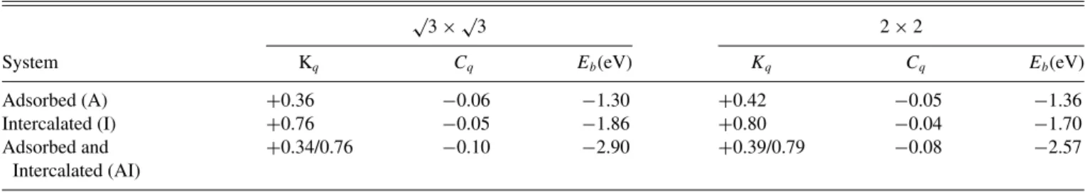
TABLE I. Kq and Cq represent the net charges on K and C atomic planes with respect to their formal charges in (√ 3×√
3) and (2×2) systems calculated using a Bader charge analysis, whileEbare the adsorption/intercalation energies of adatoms expressed in eV and calculated for all configurations, that is for adsorption and/or intercalation with respect to the graphene plane in both periodicities of K.
√3×√
3 2×2
System Kq Cq Eb(eV) Kq Cq Eb(eV)
Adsorbed (A) +0.36 −0.06 −1.30 +0.42 −0.05 −1.36
Intercalated (I) +0.76 −0.05 −1.86 +0.80 −0.04 −1.70
Adsorbed and Intercalated (AI)
+0.34/0.76 −0.10 −2.90 +0.39/0.79 −0.08 −2.57
The thermal stability of this double-side doped sample is then evaluated by heating toT =360 K. After this treatment, in the photoemission map around point, the adsorption- induced K4s band is not visible anymore, while a folded Dirac cone band appears [Fig. 4(a), right], similar to the LiC6 and CaC6 systems [23,60]. The BE of the Dirac point is reduced to 1.32±0.06 eV [Fig.4(b), right]. The diffraction pattern turns into a (√
3×√
3) reconstruction with no sign of (2×2) periodicity [Fig.4(c), right], and the relative charge transfer calculated from the Fermi surface area [Fig. 4(d) right] is reduced ton=0.043±0.005eper C atom, similar to the (√
3×√
3) configuration obtained for the experiment performed at RT. We therefore refer to this case again as Gr/K(√
3×√
3). In Fig. S4 of the Supplemental Material [55], we show that by starting from this Gr/K(√
3×√
3) system of Fig.4, right, a subsequent step of K deposition on the sample at 80 K recovers the double-side doped sample configuration with the Dirac point back to 1.61 eV and mixed (2×2) and (√
3×√
3) superstructures. This system ends again in an intercalated (√
3×√
3) phase, with Dirac point located at about 1.3 eV even with prolonged RT stage.
Our DFT calculations provide complementary insights into the experimental measurements described above. We focused on the (2×2) and (√
3×√
3) periodicities, and for each of them we considered K adsorption (labeled as A) on the graphene surface, intercalation (I) at the Gr/Ir interface, as well as coexistence of K adsorption and intercalation (AI).
We have first quantified the charge accumulat- ion(−)/depletion(+) of the K and C atoms in the different systems by Bader charge population analysis, as reported in Table I, where Kq and Cq represent the net charges on K and C atomic planes with respect to their formal charges in the two periodicities. By comparing the adsorbed and intercalated systems, this analysis confirms how intercalation induces strong charge depletion at the K atoms, while the charge on the C atoms is relatively unaffected by the actual A or I position of the K dopant. In agreement with experimental results, the charge on the C atom substantially increases (by a factor of two) only when the dopant is both above and below the graphene sheet (AI system) independently from the recon- struction. The adsorption/intercalation energies are reported in the third column of TableIfor both periodicities. The data clearly show the energetic preference for intercalation with respect to adsorption, with an energy driving force of 0.56 eV and 0.34 eV for the (√
3×√
3) and (2×2) intercalated cases, respectively. The energy of adsorption is comparable for the two coverages, while the energy of intercalation is marginally
larger (i.e., more stable) for the (√ 3×√
3) periodicity, which is consistent with the experiment. TableIalso reports the values of the AI case.
These values are used to estimate the surface free energy of adsorption/intercalation assuming that the system is in thermodynamic equilibrium with a reservoir of K atoms in the gas phase and having finite temperature and pressure. The calculated phase diagram is displayed in Fig. 5, where the free energy is reported as a function ofTfor UHV conditions (pressure of 10−11mbar). Note that the present thermodynamic analysis addresses the free energy of the stable and metastable configurations and that the energy barriers separating these configurations are not included in this theory approach. The solid and dashed lines refer to the free energy of the (2×2) and (√
3×√
3) periodicities, respectively, while the colors indicate the position of the K atoms, intercalated I (red), adsorbed A (blue), or on both sides AI (green) of graphene.
The calculated thermodynamics suggests the following. (i) At RT, the intercalated configuration with (√
3×√
3) periodicity has the lowest free energy, which is in good agreement with the LEED measurements at RT reported in Fig.2(b). We notice that at RT the energy difference between the most stable and the other competing structures is fairly small, of the order of 20 meV ˚A2, which is within the error bar of the method, estimated to be around 30 meV ˚A2. (ii) At lower temperatures (e.g., at 80 K) and in the limit of 1 ML, the intercalated (I) configurations have lower energies with respect to the adsorbed (A) ones. With reference to the measurements at T =80 K, the meaningful lines are however the adsorption
−200
−150
−100
−50 0 50 100 150
0 100 200 300 400 500 600
Gads(meV Å-2)
Temperature (K) UHV−10−11mbar
RT
I (2X2) A (2X2) AI (2X2) I (√3X√3) A (√3X√3) AI (√3X√3)
FIG. 5. Thermodynamic analysis of (√ 3×√
3) and (2×2) phases of K on Gr/Ir.
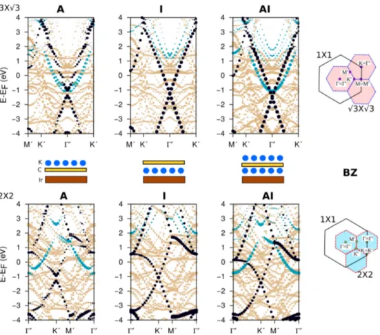
FIG. 6. Atom projected band structure (C-black, K-blue, Ir-pale brawn dots) for K adsorption and/or intercalation on Gr/Ir(111) with the (√
3×√
3) (top) and (2×2) (bottom) periodicities. A pictorial representation of the substrate, graphene, potassium arrangement is given in the middle panel for guiding the eyes. The size of the dots is proportional to the contribution of the projection on the atomic wave function of that particular state. In the right panel we depict a schematic representation of BZ supercells of the two possible reconstructions of K [blue and red dotted lines for (√
3×√
3) and (2×2) periodicity, respectively] with respect to the BZ of 1×1 graphene (black solid line).
(A) ones because, upon deposition, K will first adsorb on the graphene surface and will not diffuse to the more stable intercalated sites due to the limited mobility at this low T.
It turns out that also at T =80 K, the configuration with (√
3×√
3) periodicity has the lowest free energy, in contrast to the experimental observation that the preferred structure under these conditions has a (2×2) periodicity [Fig.3(a)]. Also in this case, the free energy difference between the (2×2)A and (√
3×√
3)A systems is very small (<20 meV ˚A2), hence we conclude that this theoretical analysis cannot be used to predict accurately the thermodynamic preference between these two competing ordered structures since their surface-free energies differ by less than the error bar we have in our calculations. (iii) At RT and in the excess of 1 ML, the calculations predict the formation of a double-side K-doped graphene, in which the K is both adsorbed and intercalated (AI), in agreement with the experimental findings. Between the (2×2)AI and (√
3×√
3)AI configurations considered in the calculations, the latter is lower in energy, and in this case the energetic preference for the (√
3×√
3)AI structure is quite large (∼50 meV ˚A2). We note that simulating systems with different K periodicities on opposite sides of graphene, such as the mixed (2×2)A/(√
3×√
3)I system, would require exceedingly large unit cells. (iv) Finally, at higher temperatures
(e.g.,T =360 K), the (√ 3×√
3)I periodicity is energetically favored, as experimentally found in Fig.4(c).
We have then focused our analysis on the atom-projected electronic band structure as a function of K doping, as displayed in Fig.6and plotted along the high-symmetry lines of the (√
3×√
3) and (2×2) supercells (depicted by blue and red dotted lines, respectively). We concentrate on potassium and graphene states, hence the electron states related to the metal substrate are shown as pale brown dots for clarity. The main goal of these band structure simulations is to illustrate how the relative energy of the K and C electron states depends on the position and coverage of the K adsorbates. To this end, as explained in the method section, the use of the small (√
3×√
3) and (2×2) supercells is more convenient than the C(10×10)/Ir(9×9) one, where the calculated bands would be multiply folded, making it difficult to recognize the usual dispersion of the graphene electron states (i.e., Dirac cone).
Due to the supercells’ BZ folding, the Dirac cone falls at the and K symmetry points of the (√
3×√
3) and (2×2) supercells, respectively. A scheme relating the high symmetry points of these BZ supercells with that of the primitive (1×1) graphene cell is included in the same figure (right panel). It is evident that both the location of the K atoms and their periodic arrangements induce considerable changes in the electronic
band structure. With respect to the pristine Gr/Ir(111) system, the K adsorption and intercalation affect the relative energy and symmetry of both the grapheneπ−π∗ (black symbols) and K4s (blue symbols) bands.
The K-derived electron states (blue symbols in Fig. 6) provide a clear fingerprint of the location and arrangement of the K dopants. Potassium adsorption leads to partial ionization and to the persistence of a metallic bonding in the (√
3×√
3) and (2×2) reconstructions. In both these cases, the Fermi level crosses the K4s bands, which display a free-electronlike parabolic shape, but the periodicity of the K layer and its relationship with the underneath graphene symmetry determines the relative position of the K4s states with respect to the Dirac cone in the graphene BZ. In the (√
3×√
3) arrangements, the K4sparabola is centered on the Dirac cone (Kpoint of the primitive graphene BZ), while it is centered on thepoint in the (2×2) K arrangement. The strong interaction of the intercalated K atoms with the metal support yields a charge transfer of about one electron per K atom to the metal. This leads to ionization and full depletion of the 4s states, which are pushed above the Fermi level by more than 1 eV. These results confirm that the intercalation is experimentally achieved in the (√
3×√
3) arrangement at RT, as reported in Fig.2, since the potassium states are not detected below the Fermi level at theKpoint. They are also consistent with a (2×2) periodicity adsorbed on graphene for the low temperature experiment as potassium states are individuated around thepoint in ARPES spectra [Fig.4(a), left].
The changes of the Fermi energy due to the electron doping are directly related to the charge analysis described above. The Dirac cone energy shifts (see Table S1 in the Supplemental Material [55]) correlate with the values of the C charge reported in Table I, and, in general, the denser (√
3×√
3) coverage leads to larger shifts than the (2×2) periodicity. The (√
3×√
3)I systems displays the largest shift of 1.25 eV, which is compatible with the measured 1.30 eV value in the experiments at RT [Fig.2(a), VII]. The (2×2)A system, relevant for the T =80 K measurements, displays a smaller shift of 1.1 eV, consistent with the data of Fig.3(b) II and III. Finally, when K is present on both sides of the graphene sheet, a significant larger energy shift of the Dirac cone is calculated up to 1.5 eV for the (√
3×√ 3)AI configuration (see Table S1 in the Supplemental Material [55]), which is comparable with the experimental value of 1.61 eV.
However, for the (√ 3×√
3)AI configuration, we should expect the potassium state crossing the Dirac cone atKpoint (Fig. 6) and a diffraction pattern showing only a (√
3×
√3) reconstruction. Nevertheless, from the experimental data described in Fig. 4, left, we have seen that for maximal doping the diffraction pattern exhibits both the (√
3×√ 3) and the (2×2) periodicities. Moreover, the parabolic K4sband appears around thepoint, which is associated to the (2×2) arrangement for adsorption or adsorption plus intercalation configurations (Fig.6). Therefore, only the mixed case, where (√
3×√
3)I and (2×2)A periodicities surround the graphene sheet, is compatible with our experimental results. Simulating this mixed (√
3×√
3)I/(2×2)A system would require using larger supercells (i.e., 6×6). The electron states computed in these supercells would present a multiply folded band structure that would hinder the comparison with the ARPES. We note
that the use of the (√ 3×√
3) and (2×2) supercells together with the DFT-D2 functional slightly overbinds Gr to the Ir surface, which results in a smaller interlayer distance (3.15 A) with respect to 3.27–3.62 ˚˚ A obtained with the C(10 × 10)/Ir(9 ×9) and vdW-DF computational setup. This leads to the opening of pseudogaps in the band structure of the pristine Gr/Ir and K/Gr/Ir systems. As displayed in Figs. S5 and S6 in the Supplemental Material [55], such features are very sensitive to small changes in the interlayer distances. Increas- ing the Gr/Ir distance by 0.1–0.2 ˚A closes these pseudogaps and recovers the agreement with band structures calculated in larger C(10×10)/Ir(9×9) computational setups [61].
IV. CONCLUSION
In the present paper, we reported on potassium doped graphene supported by Ir(111), showing that by controlling the substrate temperature during K evaporation it is possible to handle different periodicities, (2×2) or (√
3×√
3), and to achieve a mixed configuration including adsorption (KC8) and intercalation (KC6) with respect to the graphene plane. The combination of ARPES and LEED measurements showed that at RT potassium atoms are characterized by high mobility and that they intercalate between graphene and the Ir substrate forming Gr/K(√
3×√
3)/Ir, as demonstrated by the disap- pearance of moir´e reconstruction in LEED and as confirmed by DFT calculations, which indicate a large thermodynamic driving force for intercalation. The measured charge transfer from K to C atoms was n=0.041e per C atom, and the measured Dirac cone downshift, corresponding to an energy position of ED =1.30 eV, matched closely the calculated value of 1.25 eV. For deposition performed atT =80 K, the Dirac point was located at ED=1 eV, in good agreement with the calculated downshift of 1.1 eV. In parallel, a (2×2) reconstruction with moir´e superstructure appeared in LEED, thus establishing that the ordered phase was adsorbed and not intercalated, i.e., K(2×2)/Gr/Ir, as confirmed also by the appearance of K4sstates around thepoint in photoemission spectra. No substantial modifications were observed in the (2×2) diffraction pattern, and in the doping level when a K coverage exceeding monolayer was deposited, the exclusive effect was an increase in the background signal intensity. Once the sample experienced the RT annealing, the K intercalation was facilitated revealing a higher doping level with ED = 1.61 eV and a massive charge transfer ofn=0.078eper C atom, almost twice the value obtained for the RT case. Our simulations showed that such a large shift of the Dirac point is possible only when an intercalated and an adsorbed layer of K atoms coexist, and besides, our experiments indicated that the adsorbed layer has a (2×2) periodicity while the intercalated layer displays a (√
3×√
3) reconstruction. Only the intercalated (√
3×√
3) periodicity remained after the sample was heated to T =360 K, in agreement with the stability calculations performed by DFT. This analysis also showed that the K4s band is sensitive both to the position of the K layer and to its periodic arrangement. Intercalation of K leads to complete ionization of the K atoms, resulting in a shift of the K4sband over the Fermi level, while adsorption results in incomplete ionization and a partially filled band. The minimum of the 4sband coincides with the location of the Dirac point
in the case of the (√ 3×√
3) periodicity, while this is not the case for the (2×2) periodicity. Therefore, the K4sband can be used as an indicator to determine the periodicity and location of the K layers.
ACKNOWLEDGMENTS
C.S. and L.P. thank AREA Science Park Trieste (Training Grant 2012) and the European Cooperation in Science and Technology (COST) Action MP0901 (STSM Grant) for partial
financial support and D. Lonza for technical assistance. C.S.
is grateful to the Belgian Fund for Scientific Research (FRS- FNRS) for its financial support through the grant Fonds pour la Formation `a la Recherche dans l’Industrie et dans l’Agriculture (FRIA). M.S. is a FRS-FNRS Postdoctoral Researcher. N.V.
acknowledges the Austrian Science Fund (FWF) Project No. P27769-N20—‘Electron and Spin Correlation in Nano Carbon-Metal Hybrids’, and the Russian Science Foundation (Grant No. 14-13-00747). A.G. acknowledges the European Research Council (ERC) Grant No. 648589—‘SUPER-2D’.
[1] A. K. Geim and K. S. Novoselov,Nat. Mater.6,183(2007).
[2] G. Eda and M. Chhowalla,Adv. Mater.22,2392(2010).
[3] T. Ohta, A. Bostwick, T. Seyller, K. Horn, and E. Rotenberg, Science313,951(2006).
[4] R. R. Nair, W. Ren, R. Jalil, I. Riaz, V. G. Kravets, L. Britnell, P. Blake, F. Schedin, A. S. Mayorov, S. Yuan, M. I. Katsnelson, H.-M. Cheng, W. Strupinski, L. G. Bulusheva, A. V Okotrub, I. V Grigorieva, A. N. Grigorenko, K. S. Novoselov, and A. K.
Geim,Small6,2877(2010).
[5] D. Haberer, L. Petaccia, M. Farjam, S. Taioli, S. A. Jafari, A.
Nefedov, W. Zhang, L. Calliari, G. Scarduelli, B. Dora, D. V.
Vyalikh, T. Pichler, C. W¨oll, D. Alf`e, S. Simonucci, M. S.
Dresselhaus, M. Knupfer, B. B¨uchner, and A. Gr¨uneis,Phys.
Rev. B83,165433(2011).
[6] R. Faccio, L. Fern´andez-werner, H. Pardo, and C. Goyenola,J.
Phys. Chem. C114,18961(2010).
[7] D. Usachov, O. Vilkov, A. Gr¨uneis, D. Haberer, A. Fedorov, V. K. Adamchuk, A. B. Preobrajenski, P. Dudin, A. Barinov, M.
Oehzelt, C. Laubschat, and D. V Vyalikh,Nano Lett.11,5401 (2011).
[8] M. Scardamaglia, B. Aleman, M. Amati, C. Ewels, P. Pochet, N. Reckinger, J.-F. Colomer, T. Skaltsas, N. Tagmatarchis, R.
Snyders, L. Gregoratti, and C. Bittencourt,Carbon N. Y.73,371 (2014).
[9] Y. H. Lu, W. Chen, Y. P. Feng, and P. M. He,J. Phys. Chem. B 113,2(2009).
[10] M. Scardamaglia, C. Struzzi, S. Lizzit, M. Dalmiglio, P. Lacovig, A. Baraldi, C. Mariani, and M. G. Betti,Langmuir29,10440 (2013).
[11] A. V Fedorov, N. I. Verbitskiy, D. Haberer, C. Struzzi, L.
Petaccia, D. Usachov, O. Y. Vilkov, D. V Vyalikh, J. Fink, M.
Knupfer, B. B¨uchner, and A. Gr¨uneis,Nat. Commun.5,3257 (2014).
[12] V. S. Robinson, T. S. Fisher, J. A. Michel, and C. M. Lukehart, Appl. Phys. Lett.87,061501(2005).
[13] M. Salvato, M. Lucci, I. Ottaviani, M. Cirillo, E. Tamburri, I.
Cianchetta, V. Guglielmotti, S. Orlanducci, M. L. Terranova, and M. Pasquali,Phys. Rev. B84,233406(2011).
[14] C. Kramberger, H. Rauf, M. Knupfer, H. Shiozawa, D. Batchelor, A. Rubio, H. Kataura, and T. Pichler,Phys. Rev.
B79,195442(2009).
[15] A. Claye, S. Rahman, J. E. Fischer, A. Sirenko, and G. U.
Sumanasekera,Chem. Phys. Lett.333,16(2001).
[16] X. Liu, T. Pichler, M. Knupfer, and J. Fink,Phys. Rev. B67, 125403(2003).
[17] C. Struzzi, D. Erbahar, M. Scardamaglia, M. Amati, L. Gregoratti, M. J. Lagos, G. Van Tendeloo, R. Snyders, C.
Ewels, and C. Bittencourt,J. Mater. Chem. C3,2518(2015).
[18] A. Hazra and I. N. Basumallick, J. New Mat. Electrochem.
Systems5, 53 (2002).
[19] A. Gr¨uneis, C. Attaccalite, A. Rubio, D. V. Vyalikh, S. L.
Molodtsov, J. Fink, R. Follath, W. Eberhardt, B. B¨uchner, and T. Pichler,Phys. Rev. B80,075431(2009).
[20] J. Renard, M. B. Lundeberg, J. A. Folk, and Y. Pennec,Phys.
Rev. Lett.106,156101(2011).
[21] M. Bianchi, E. D. L. Rienks, S. Lizzit, A. Baraldi, R. Balog, L.
Hornekær, and P. Hofmann,Phys. Rev. B81,041403(R) (2010).
[22] I. Pletikosi´c, M. Kralj, M. Milun, and P. Pervan,Phys. Rev. B 85,155447(2012).
[23] G. Profeta, M. Calandra, and F. Mauri,Nat. Phys.8,131(2012).
[24] M. Papagno, S. Rusponi, P. M. Sheverdyaeva, S. Vlaic, M.
Etzkorn, D. Pacil´e, P. Moras, C. Carbone, and H. Brune,ACS Nano6,199(2012).
[25] M. Petrovi´c, I. ˇSrut Raki´c, S. Runte, C. Busse, J. T. Sadowski, P. Lazi´c, I. Pletikosi´c, Z.-H. Pan, M. Milun, P. Pervan, N.
Atodiresei, R. Brako, D. ˇSokˇcevi´c, T. Valla, T. Michely, and M. Kralj,Nat. Commun.4,2772(2013).
[26] P. Pervan, P. Lazi´c, M. Petrovi´c, I. ˇSrut Raki´c, I. Pletikosi´c, M.
Kralj, M. Milun, and T. Valla,Phys. Rev. B92,245415(2015).
[27] P. Bennich, C. Puglia, A. Br¨uhwiler, A. Nilsson, A. J. Maxwell, A. Sandell, N. Ma, and P. Rudolf,Phys. Rev. B59,8292(1999).
[28] M. Caragiu and S. Finberg,J. Phys.: Condens. Matter17,R995 (2005).
[29] M. Calandra and F. Mauri, Phys. Rev. Lett. 95, 237002 (2005).
[30] T. Kihlgren, T. Balasubramanian, L. Walld´en, and R. Yakimova, Surf. Sci.600,1160(2006).
[31] L. ¨Osterlund, D. V. Chakarov, and B. Kasemo,Surf. Sci.420, 174(1999).
[32] S. Schumacher, T. O. Wehling, P. Lazi´c, S. Runte, D. F. F¨orster, C. Busse, M. Petrovi´c, M. Kralj, S. Bl¨ugel, N. Atodiresei, V.
Caciuc, and T. Michely,Nano Lett.13,5013(2013).
[33] J. Kleeman, K. Sugawara, T. Sato, and T. Takahashi,Phys. Rev.
B87,195401(2013).
[34] Z.-H. Pan, J. Camacho, M. H. Upton, A. V. Fedorov, C. A.
Howard, M. Ellerby, and T. Valla,Phys. Rev. Lett.106,187002 (2011).
[35] S.-L. Yang, J. A. Sobota, C. A. Howard, C. J. Pickard, M.
Hashimoto, D. H. Lu, S.-K. Mo, P. S. Kirchmann, and Z.-X.
Shen,Nat. Commun.5,3493(2014).
[36] Z. Li, K. M. Hock, and R. E. Palmer,Phys. Rev. Lett.67,12 (1991).
[37] J. C. Barnard, K. M. Hock, and R. E. Palmer,Surf. Sci.287-288, 178(1993).
[38] N. J. Wu and A. Ignatiev,J. Vac. Sci. Technol.20,896(1982).
[39] D. Haberer, L. Petaccia, A. V. Fedorov, C. S. Praveen, S. Fabris, S. Piccinin, O. Vilkov, D. V. Vyalikh, A. Preobrajenski, N. I.
Verbitskiy, H. Shiozawa, J. Fink, M. Knupfer, B. B¨uchner, and A. Gr¨uneis,Phys. Rev. B88,081401(R) (2013).
[40] J. M. Luttinger,Phys. Rev.119,1153(1960).
[41] L. Boeri, G. Bachelet, M. Giantomassi, and O. Andersen,Phys.
Rev. B76,064510(2007).
[42] C. Struzzi, N. I. Verbitskiy, A. V. Fedorov, A. Nefedov, O. Frank, M. Kalbac, G. Di Santo, M. Panighel, A. Goldoni, J. G¨artner, W.
Weber, M. Weinl, M. Schreck, C. W¨oll, H. Sachdev, A. Gr¨uneis, and L. Petaccia,Carbon N. Y.81,167(2015).
[43] L. Petaccia, P. Vilmercati, S. Gorovikov, M. Barnaba, A. Bianco, D. Cocco, C. Masciovecchio, and A. Goldoni,Nucl. Instrum.
Methods A606,780(2009).
[44] J. P. Perdew, K. Burke, and M. Ernzerhof,Phys. Rev. Lett.77, 3865(1996).
[45] P. Giannozzi, S. Baroni, N. Bonini, M. Calandra, R. Car, C.
Cavazzoni, D. Ceresoli, G. L. Chiarotti, M. Cococcioni, I. Dabo, A. Dal Corso, S. de Gironcoli, S. Fabris, G. Fratesi, R. Gebauer, U. Gerstmann, C. Gougoussis, A. Kokalj, M. Lazzeri, L. Martin- Samoset al.,J. Phys.: Condens. Matter21,395502(2009).
[46] http://www.quantum-espresso.org/pseudopotentials/.
[47] S. Grimme,J. Comput. Chem.27,1787(2006).
[48] C. S. Praveen, S. Piccinin, and S. Fabris,Phys. Rev. B92,075403 (2015).
[49] C. Busse, P. Lazi´c, R. Djemour, J. Coraux, T. Gerber, N.
Atodiresei, V. Caciuc, R. Brako, A. T. N’Diaye, S. Bl¨ugel, J. Zegenhagen, and T. Michely,Phys. Rev. Lett.107,036101 (2011).
[50] W. Ku, T. Berlijn, and C. C. Lee,Phys. Rev. Lett.104,216401 (2010).
[51] D. F. F¨orster, T. O. Wehling, S. Schumacher, A. Rosch, and T.
Michely,New J. Phys.14,023022(2012).
[52] M. Vanin, J. Mortensen, A. Kelkkanen, J. Garcia-Lastra, K.
Thygesen, and K. Jacobsen, Phys. Rev. B 81, 081408(R) (2010).
[53] K. Reuter and M. Scheffler, Phys. Rev. B 65, 035406 (2001).
[54] A. Gr¨uneis, C. Attaccalite, A. Rubio, D. Vyalikh, S. Molodtsov, J. Fink, R. Follath, W. Eberhardt, B. B¨uchner, and T. Pichler, Phys. Rev. B79,205106(2009).
[55] See Supplemental Material athttp://link.aps.org/supplemental/
10.1103/PhysRevB.94.085427 for further details on the ab- initio thermodynamic analysis, on the calculated Dirac cone shift (band structure) vs potassium coverage (interlayer C-Ir distance), and on the experimental data as a function of potassium coverage atT =80 K and subsequent annealing up toT =360 K.
[56] M. Dresselhaus, G. Dresselhaus, and J. Fischer,Phys. Rev. B 15,3180(1977).
[57] A. Gr¨uneis, C. Attaccalite, L. Wirtz, H. Shiozawa, R.
Saito, T. Pichler, and A. Rubio, Phys. Rev. B 78, 205425 (2008).
[58] J. L. McChesney, A. Bostwick, T. Ohta, T. Seyller, K. Horn, J. Gonz´alez, and E. Rotenberg,Phys. Rev. Lett.104, 136803 (2010).
[59] H. Vita, S. B¨ottcher, K. Horn, E. N. Voloshina, R. E.
Ovcharenko, T. Kampen, A. Thissen, and Y. S. Dedkov, Sci.
Rep.4,5704(2014).
[60] K. Kanetani, K. Sugawara, T. Sato, R. Shimizu, K. Iwaya, T.
Hitosugi, and T. Takahashi,PNAS109,19610(2012).
[61] Y. Dedkov and E. Voloshina,J. Phys.: Condens. Matter 27, 303002(2015).