D is se rt at io ns re ih e P hy si k - B an d 4 1 Johannes Kar ch
Suspended Carbon Nanotubes as Electronical and Nano-Electro- Mechanical Hybrid Systems in the Quantum Limit
Daniel R. Schmid
41
9 783868 451115
ISBN 978-3-86845-111-5
Daniel R. Schmid
ISBN 978-3-86845-111-5
for the investigation of the interplay with their mechanical vibra- tion in the quantum limit. Within the scope of this thesis both excelling electronical and mechanical properties of carbon na- notubes clamped between metal contacts have been investigated.
At cryogenic temperatures a quantum dot is formed on the sus- pended part of the nanotube, where ground and excited state spectroscopy could be performed. Here one has access even to the very first electron on the quantum dot, where the magnetic field dependence of the excited states directly provides the single par- ticle energy spectrum. Curvature induced spin-orbit coupling and KK’ valley mixing lift the carbon nanotube specific fourfold de- generacy and induce a level splitting giving rise to unconventional Kondo resonances in the intermediate coupling regime. Tracing those resonances in dependence on an external magnetic field re- veals a hitherto unobserved many-body selection rule based on the discrete symmetries of the electronic carbon nanotube system.
In addition, the transversal vibration mode of this doubly clamped nano-resonator is actuated and detected, and is used to probe the dependence of the mechanical vibration on the quantum dot charg- ing state and on an external magnetic field. Due to the high me- chanical quality the electromechanical coupling in different trans- port regimes could be analyzed in high precision.
as Electronical and Nano-Electro- Mechanical Hybrid Systems in the Quantum Limit
Herausgegeben vom Präsidium des Alumnivereins der Physikalischen Fakultät:
Klaus Richter, Andreas Schäfer, Werner Wegscheider, Dieter Weiss
Dissertationsreihe der Fakultät für Physik der Universität Regensburg, Band 41
Hybrid Systems in the Quantum Limit
Dissertation zur Erlangung des Doktorgrades der Naturwissenschaften (Dr. rer. nat.) der naturwissenschaftlichen Fakultät II - Physik der Universität Regensburg vorgelegt von
Daniel R. Schmid aus Möning im Jahr 2014
Die Arbeit wurde von Dr. Andreas K. Hüttel angeleitet.
Das Promotionsgesuch wurde am 27.11.2014 eingereicht.
Das Kolloquium fand am 02.06.2014 statt.
Prüfungsausschuss: Vorsitzender: Prof. Dr. Tilo Wettig 1. Gutachter: Dr. Andreas K. Hüttel 2. Gutachter: Prof. Dr. Jascha Repp weiterer Prüfer: Prof. Dr. Rupert Huber
as Electronical and Nano-Electro-
Mechanical Hybrid Systems in the
Quantum Limit
in der Deutschen Nationalbibliografie. Detailierte bibliografische Daten sind im Internet über http://dnb.ddb.de abrufbar.
1. Auflage 2014
© 2014 Universitätsverlag, Regensburg Leibnizstraße 13, 93055 Regensburg Konzeption: Thomas Geiger
Umschlagentwurf: Franz Stadler, Designcooperative Nittenau eG Layout: Daniel R. Schmid
Druck: Docupoint, Magdeburg ISBN: 978-3-86845-111-5
Alle Rechte vorbehalten. Ohne ausdrückliche Genehmigung des Verlags ist es nicht gestattet, dieses Buch oder Teile daraus auf fototechnischem oder elektronischem Weg zu vervielfältigen.
Weitere Informationen zum Verlagsprogramm erhalten Sie unter:
www.univerlag-regensburg.de
F¨ ur meine Familie
500nm
List of Tables xi
List of Figures xvi
List of Symbols xvii
1 Introduction 1
2 Fabrication of ultra-clean suspended single-wall carbon nanotubes 5
3 Properties of carbon nanotubes 11
3.1 From graphene to carbon nanotubes . . . 12
3.2 Electronical properties of carbon nanotube quantum dots . . . 17
3.2.1 From classical to quantum Coulomb blockade . . . 17
3.2.2 Influence of spin-orbit coupling, KK0-mixing, and magnetic fields on the quantum dot levels . . . 21
3.3 Quantum dot spectroscopy . . . 24
4 The Kondo effect in quantum dots 33 5 Electronic spectroscopy of ultra-clean carbon nanotube quantum dots 37 5.1 Single particle spectrum in the presence of spin-orbit coupling and KK0-mixing . . . 38
5.1.1 Angle calibration . . . 38
5.1.2 Parallel magnetic field . . . 39
5.1.3 Linear low field range . . . 42
5.1.4 High field range . . . 45
5.2 Kondo spectroscopy of CNT quantum dot with finite spin-orbit cou- pling and KK0-mixing . . . 47
5.2.1 Theory of Kondo transitions and selection rules . . . 48
ix
5.2.2 Characterization of the Kondo effect at zero field . . . 53
5.2.3 Evolution of the Kondo resonances in a perpendicular mag- netic field . . . 54
5.2.4 Evolution of the Kondo resonances in a parallel magnetic field 57 5.2.5 Modeling with non-equilibrium many-particle theory . . . 61
5.3 Additionally recorded data . . . 64
5.3.1 Two electron spectrum . . . 64
5.3.2 Magnetic field effect on the conductance in the Kondo regime 67 5.3.3 Hole conduction . . . 69
6 Nanoelectromechanics with CNTs 71 6.1 Theoretical background of CNT nano-electro-mechanical systems . . . 72
6.1.1 Actuation of mechanical vibration in suspended CNTs . . . 72
6.1.2 Continuum mechanics of the transversal bending mode in car- bon nanotubes . . . 75
6.1.3 Detection mechanism via dc-current measurement through an embedded quantum dot . . . 76
6.1.4 Dependence of resonance frequency on quantum dot charging . 79 6.2 Magnetic damping of a driven CNT resonator . . . 85
6.3 Charge detection in the Kondo regime . . . 92
6.4 Estimation of the amplitude of the CNT oscillation . . . 97
7 Superconducting microwave resonators 101 7.1 Motivation . . . 101
7.2 Microwave engineering . . . 102
7.3 Micro-fabrication of superconducting coplanar-waveguide resonators . 105 7.4 Measurement setup . . . 107
7.5 Measurements and results . . . 109
7.5.1 Superconducting films . . . 109
7.5.2 RF measurements on sc-cpw resonators . . . 109
8 Conclusion and Outlook 113 A CNT fabrication 117 A.1 Optical lithography . . . 117
A.2 Electron beam lithography . . . 117
A.3 Metallization and reactive ion etching . . . 118
A.4 Catalyst for the carbon nanotube growth . . . 118
A.5 Chemical vapor deposition growth process . . . 119
B Assignment of the cool-downs to the different
measurement setups 121
C Fabrication of sc-cpw resonators 123
C.1 Co-sputtering ReMo-alloys . . . 123 C.2 Reactive ion etching . . . 124
D HF-equipment 125
Bibliography 127
Curriculum Vitae 137
3.1 Transport regimes for a conducting island coupled to leads . . . 18
5.1 Best fit CNT QD parameters for Nel = 1 . . . 44
5.2 Best fit CNT QD parameters for Nel = 21 . . . 57
5.3 Best fit CNT QD parameters for Nel = 17 . . . 59
7.1 Sample parameters of the cpw resonators . . . 106
A.1 Recipe of the SiOx reactive ion etching process . . . 118
A.2 CNT growth catalyst composition . . . 118
B.1 Specification of the cool-downs . . . 121
C.1 Sputtering parameters for the Re70Mo30 alloy . . . 123
C.2 Recipe of the reactive ion etching of ReMo . . . 124
xiii
2.1 Suspended CNT sample fabrication overview . . . 6 2.2 Optical mask design and optical microscope picture of coarse electrode
structures . . . 7 2.3 Electron beam lithography design for the carbon nanotube electrode
geometry . . . 8 2.4 Scanning electron microscope picture of the electrode structure . . . . 9 2.5 Scanning electron microscope picture of a suspended carbon nanotube 9 3.1 Graphene lattice in real and reciprocal space . . . 12 3.2 Energy dispersion of theπband in graphene with a detail view of one
Dirac cone . . . 13 3.3 Unit cell of a (6,4) carbon nanotube . . . 14 3.4 Exemplary calculated dispersion of a (3,3) CNT . . . 16 3.5 Sketches of conductance traces G(Vg) for different CNT types . . . . 17 3.6 Replacement circuit of a gate controlled quantum dot coupled to a
source and a drain lead . . . 19 3.7 Longitudinal quantization levels on a CNT subband . . . 20 3.8 Single particle level spectrum of a CNT longitudinal mode in perpen-
dicular and parallel magnetic fields . . . 23 3.9 Measurement setup for electronic spectroscopy . . . 24 3.10 Energy diagrams for the case of single electron tunneling and Coulomb
blockade . . . 27 3.11 Gate dependence of the current I(Vg) through a carbon nanotube
quantum dot atT=300 mK . . . 28 3.12 Detail of Fig. 3.11 at few electrons, showing fourfold periodicity . . . 29 3.13 Stability diagram for 0 ≤Nel ≤6 at T=30 mK and of the first holes
atT=300 mK . . . 30 4.1 Transport processes for spin-1/2-Kondo effect in quantum dots . . . . 34 4.2 Temperature dependence of dI/dVsd(Vg) in the Kondo regime . . . . 34
xv
4.3 Stability diagram dI/dVsd(Vg, Vsd) in the intermediate coupling regime (18≤Nel ≤22) showing sharp zero-bias Kondo ridges . . . 35 4.4 Higher order tunnel processes for spin and orbital Kondo effect in
quantum dots . . . 36 5.1 Calibration measurement I(θ, Vg) of the magnetic field orientation
relative to the nanotube axis . . . 39 5.2 Stability diagrams of the first Coulomb oscillation (0 < Nel < 1) at
different magnetic fields parallel to the nanotube axis . . . 40 5.3 Magnetic field dependence of the bias trace G(Vsd) through the first
diamond for Bk <2 T . . . 41 5.4 Fitting the first electron excited states with single-electron theory . . 44 5.5 Magnetic field dependence of the bias trace G(Vsd) through the first
diamond in high field Bk <17 T . . . 45 5.6 Fit of the high field single electron spectroscopy measurement . . . . 46 5.7 Gate dependence of the differential conductance at low bias voltage
Vsd = 0.2 mV and low temperature T = 30 mK . . . 47 5.8 Bias traces G(Vsd) for different fixed Nel . . . 49 5.9 Magnetic field dependence and symmetry conjugations of the CNT
eigenstates for finite spin-orbit coupling and valley mixing . . . 50 5.10 Elastic and inelastic Kondo transitions . . . 52 5.11 Stability diagram forNel = 21 with rescaled bias traces and extracted
Kondo temperatures . . . 53 5.12 Magnetic field dependence of the bias trace G(Vsd) at Nel = 21 in
perpendicular orientation to the CNT axis . . . 54 5.13 Determination of the gs0-factor by linear fitting of the central peak
splitting . . . 55 5.14 Fitting of the peak positions with the single-particle energy spectrum
in a perpendicular field . . . 56 5.15 Differential conductance in dependence on a parallel field and on the
bias voltage for Nel= 17 . . . 57 5.16 Fitting of the peak positions with the single-particle energy spectrum
in a parallel field . . . 60 5.17 Temperature dependence of measured and calculated conductance
traces . . . 61 5.18 Magnetic field dependence of measured and calculated conductance
traces for both perpendicular and parallel field orientation . . . 63 5.19 Stability diagram of the second Coulomb oscillation and conductance
traces G(Vsd) in parallel field dependence . . . 66
5.20 Gate dependence of the current as function of a parallel magnetic field for 32< Nel <48 . . . 68 5.21 Parallel magnetic field dependence of conductance traces G(Vg) for
Nh<10 . . . 70 6.1 Length dependence of the energy for different CNT vibration modes . 72 6.2 Stability diagram for 1< Nel <2 with hints of longitudinal vibration
modes . . . 73 6.3 3He evaporation cryostat with an installed rf-antenna . . . 75 6.4 Detection mechanism for CNT transversal vibrations . . . 77 6.5 Power dependence of the frequency dependence of the averaged dc-
current around a mechanical resonance . . . 78 6.6 Gate voltage dependence of the mechanical resonance frequency on
large scale . . . 80 6.7 Gate dependence of the resonance frequency aroundNel = 19 . . . 82 6.8 Sketch of the bias dependence off0(Vg) for low and high tunnel
rates Γ . . . 83 6.9 Resonance frequency behavior in the few electron regime 0≤Nel ≤3 83 6.10 Resonance frequency behavior for few hole charging states . . . 84 6.11 Stability diagram for high electron numbers around Nel = 40 showing
discontinuities in the conductance . . . 85 6.12 Stability diagram around Nel = 40 with damped mechanical effects . . 86 6.13 Theoretically calculated current modification in the strong feedback
regime . . . 86 6.14 Numerically obtained conductance in the self-excitation area at dif-
ferent magnetic fields . . . 87 6.15 Circuit model explaining magnetic damping . . . 88 6.16 Dependence of the quality factor Q on an external magnetic field . . 90 6.17 Theoretically proved magnetic field dependence of the Q-factor . . . . 91 6.18 Gate dependence of the differential conductance in the electron con-
duction regime . . . 92 6.19 Mean current as function of gate voltage and driving frequency in the
strong Kondo regime . . . 93 6.20 Measured and calculated gate dependence of the resonance frequency
f0(Vg) and the current I(Vg) . . . 96 6.21 Stability diagram around Nel = 40 atB = 0 T and B = 2 T . . . 97 6.22 Current|I|(Vg) in the self-oscillation region for un-damped and damped
mechanical vibration . . . 98
7.1 Current density and electric field distribution in cpw-structures . . . 103
7.2 Sketch of half- and quarter-wavelength coplanar waveguide resonators 104 7.3 Cpw resonator fabrication overview . . . 105
7.4 Sketch and SEM images of a quarter-wavelength resonator . . . 107
7.5 Sketch and picture of the HF sample holder . . . 108
7.6 Sketch of the HF measurement setup . . . 108
7.7 Temperature dependence of the Re and ReMo alloy resistance before and after the CVD process . . . 109
7.8 Frequency dependence of the attenuation of quarter-wavelength res- onators . . . 110
7.9 Attenuation of a quarter-wavelength resonator as a function of rf- frequency and input power . . . 112
D.1 Rohde+Schwarz Signal Generator and Analyzer . . . 125
D.2 High frequency dipstick assembly . . . 126
a Lattice constant of graphene (a= 2.46·10−10m) . . . 12
~a1,2 Unit vectors of the hexagonal graphene lattice . . . 12
α Gate coupling factor . . . 25
B~ External magnetic field (B =|B~|) . . . 21
B⊥,k Perpendicular and parallel component of the external magnetic field . . . 21
~b1,2 Reciprocal unit vectors of the hexagonal graphene lattice . . . 12
c Speed of light in vacuum (c= 1/√ 0µ0 '2.998·108m/s) . . . 103
C~ Chiral vector in carbon nanotubes (CNTs) . . . 12
Cˆ Chiral symmetry operator . . . 48
C Capacitance of a stripline per unit length . . . 103
Cg,S,D,Σ Gate, source, drain, and total capacitance of a quantum dot . . . 18
∆ Energy distance between Kramers doublets in one longitudinal mode of a CNT quantum dot (QD) . . . 22
∆k Energy distance between different longitudinal modes in a CNT QD . . . 42
∆ Single particle quantum energy . . . 19
∆E Addition energy: energy required to charge a quantum dot with an additional electron . . . 19
∆k⊥ Subband spacing of a CNT in the Brillouin zone of graphene . . . 15
∆kk Longitudinal quantization induced spacing within one CNT subband . . . 43
∆KK’ KK0 splitting . . . 23
∆SO Spin-orbit splitting . . . 23
e Elementary electric charge (e'1.602·10−16A s) . . . 18
EC Classical charging energy of a quantum dot . . . 18
Eg Size of the semiconducting energy gap . . . 16
xix
Relative dielectric constant . . . 103
0 Vacuum permittivity (0 '8.854·10−12A s/(V m)) . . . 103
eff Effective dielectric constant . . . 103
εd Reference energy of the longitudinal mode of a CNT QD . . . 21
ε1,2,3,4 Eigenenergies of the levels in one CNT QD quadruplet . . . 48
f Frequency of the rf-signal . . . 80
φ Angle between CNT axis and external magnetic field . . . 21
φ0 Magnetic flux quantum (φ0 '2.068·103T/nm2) . . . 43
G Differential conductance, i.e. derivative of the current with respect to the bias voltage (G≡dI/dVsd) . . . 25
G0 Differential conductance at zero bias voltage Vsd = 0 . . . 35
ΓS,ΓD Tunnel rate to source (S) and drain (D) lead . . . 18
gorb Orbital g-factor . . . 22
gs Spin g-factor . . . .22
g0s Effective spin g-factor . . . 55
~ Reduced Planck constant (~≡h/(2π)'6.582·10−16eV s) . . . 38
I Electric current through the quantum dot . . . 25
kB Boltzmann constant (kB '8.617·10−5eV/K) . . . 17
kk Longitudinal quantization direction in the k-space of a CNT . . . 15
k⊥ Transversal quantization direction in the k-space of a CNT . . . 15
K, K0 Dirac points in the reciprocal graphene lattice . . . 13
λ Wavelength of an rf-signal . . . 104
λF Fermi wavelength . . . 19
L Inductance of a stripline per unit length . . . 103
Lk Kinetic inductance of a superconducting stripline per unit length 102 Lm Geometric inductance of a stripline per unit length . . . 102
µ Electro-chemical potential of the quantum dot . . . 25
µ0 Vaccum permeability (µ0 = 4π·10−7V s/(A m)) . . . 103
µB Bohr magneton (µB '5.788·10−5eV/T) . . . 22
µorb Orbital magnetic moment . . . 42
µS,D Electro-chemical potential of the source, drain electrode . . . 25
n, m Chiral indices of a carbon nanotube . . . 13 hNi Average charge occupation of the quantum dot . . . 79 Nel Number of electrons on the quantum dot . . . 35 Nh Number of holes on the quantum dot . . . 69 ω0 Mechanical resonance frequency (ω0 = 2πf0) . . . 71 Pˆ Particle-hole symmetry operator . . . 48 Prf Nominal power of an rf-signal . . . 78 Q Quality factor of a resonator . . . 71 qc Control charge (qc =CgVg) . . . .77 RK Von-Klitzing constant (RK '25812.807 V/A) . . . 71 ˆ
σx,y,z Pauli spin matrices . . . 21 T Sample temperature . . . 18 T~ Translation vector in the CNT unit cell . . . 18 Tˆ Time-reversal symmetry operator . . . 48 T0 Residual mechanical tension at charge neutrality . . . 76 Tdc Static mechanical tension . . . 76 TC Superconducting critical temperature . . . 102 TK Kondo temperature . . . 33 Vg Gate voltage applied to substrate . . . 24 Vsd Bias voltage applied between source and drain contact . . . 24 vF Fermi velocity in carbon nanotubes . . . 43 xZP Zero-point motion amplitude of a resonator . . . 71 Z Electrical impedance per unit length . . . 103
Introduction
Nano-electromechanical systems (NEMS) are promising objects both for technolog- ical advancement and fundamental physical research [Cleland, 2003]. Regarding the size they represent the next logical step after micro-electromechanical systems (MEMS), which are already widely used as force sensors resulting in very compact, sensitive and cheap devices. MEMS can by now be found in many commercial ap- plications, from acceleration sensors in smartphones or airbag trigger systems to cantilevers in scanning microscopes.
The further miniaturization to the nano-scale reaches a limit where quantum effects become dominating. The confinement of the electronic wavefunction and charge quantization introduce novel effects, and superposition and entanglement may oc- cur.
A basic condition for the observation of such quantum mechanical effects is the de- coupling of the system from its environment, which would provide thermal energy that exceeds the energy difference of the quantum states. The lowest energetic exci- tation in NEMSs is the mechanical oscillation. Such that the corresponding energy scale, which is proportional to the resonance frequency, exceeds the thermal energy, experiments must target an increase of the resonance frequency in combination with low sample temperatures. The manipulation and readout of the state without in- ducing noise, which causes demolition of the quantum state, is only possible by the coupling of the NEMS to an additional quantum system. This can transfer exci- tation quanta to the object and vice versa, as recently shown by [O’Connell et al., 2008].
Here, it is shown that ultra-clean single-wall carbon nanotubes (CNTs) can act as nearly ultimate NEMSs with diameters down to 1 nm and very low mass densities combined with a high stiffness. A detailed analysis of both electronical and mechan- ical aspects of this system is done.
Multi-wall carbon nanotubes, a concentric arrangement of several CNTs, have been
1
first observed in [Radushkevich and Lukyanovich, 1952]. In 1991 S. Iijima examined the reaction products from an electric discharge on a graphite electrode and iden- tified individual single-wall CNTs [Iijima, 1991], hollow cylinders of one-atom-thick sheets of carbon atoms arranged in a graphene lattice structure.
Following transport measurements on contacted ropes of carbon nanotubes [Bock- rath et al., 1997], Tans et al. have addressed single CNTs with metallic leads for transport measurements at low temperatures [Tans et al., 1997]. Due to tunnel barriers between CNT and metal contact the originally one-dimensional electronic system is further restricted to form a quantum dot.
In these first measurements, CNTs have been deposited on a chip substrate either from a suspension or by an on-chip growth. In the first scenario, nanotubes are synthesized separately by laser evaporation or electrical discharge and collected in a solvent, while in the latter method the CNTs are grown directly on the chip, based on a chemical vapor deposition process. The various methods are listed in [Saito R.;
Dresselhaus G, 1998]. For both the fabrication of electrically contacted nanotubes starts with single CNTs fixed on the substrate by van-der-Waals forces, where they have to be located for further processing. The subsequent fabrication steps include wet chemistry and lithographic processing. Both contamination by adsorbates and damaging of the nanotubes can take place. By shifting the growth process to the very last step of the fabrication the risk of damaging and contaminating the CNT is minimized, providing so-called ”ultra-clean”, defect-free CNTs. This improves both electronic and mechanical performance [Cao et al., 2005]. A drawback is the low yield of successfully overgrown CNTs connecting two or more contacts, which can however be resolved by fabricating large arrays of contact structures on one single chip.
On the one hand the low mass density and the high Young’s modulus causes very high resonance frequencies in the MHz regime combined with very high Q-factors up to 105 [H¨uttel et al., 2009b] for defect-free nanotubes. On the other hand clean CNTs show an unperturbed electronic structure in transport spectroscopy, since they are free of defects. This provides a clean and regular level structure where the small lateral dimensions provide an sufficiently large energy spacing, resolvable by electronic spectroscopy at cryogenic temperatures.
The thesis starts with the introduction of the new fabrication method in Regensburg to achieve such ultra-clean CNTs. This results in very clean samples, meaning the absence of contaminations affecting the electronic properties. An overview of the theoretical background of the electronic structure of CNTs and the basic physics of quantum dots (QDs) is given in Chapter 3, and the Kondo effect in such QDs is introduced (see Chapter 4). Chapter 5 presents the measurements of purely elec-
tronical properties, while Chapter 6 focuses on the mechanical characteristics and the corresponding experiments, enabled by the suspended structure of the CNT sam- ple. Both the electronic spectroscopy and the mechanical measurements have been performed on one sample, i.e. on the same suspended CNT. The results are however obtained from different cool-downs in different cryostats. In Chapter 7, the progress on superconducting electronical resonators is presented, namely the fabrication and basic high frequency measurements. Finally the thesis is concluded and an outlook is given for possible future projects which are of high interest in the current research, building on the work presented here.
Fabrication of ultra-clean
suspended single-wall carbon nanotubes
In order to achieve an excelling mechanical and electronical performance of the car- bon nanotubes, a modified fabrication process following [Cao et al., 2005] is used, where the CNT growth takes place as very last step in the fabrication. This avoids any contamination by contact with chemicals as e.g. lithography resist or acids and thus keeps the nanotubes as clean as possible. Since the position of the nanotubes on the chip surface is not determined via scanning electron microscope (SEM) imag- ing, we further avoid amorphous carbon deposition on the CNT, which stems from remaining hydrocarbon gases in the SEM chamber cracked by the highly energetic electrons.
In Fig. 2.1, an overview of the discussed fabrication steps is given, which are de- scribed in the following in detail.
Chip fabrication starts with a highly positive (boron) doped silicon substrate with a thermally grown 300 nm thick silicon oxide (SiOx) layer on top. The degenerately doped semiconducting substrate guarantees electrical conductance even at temper- atures in the mK-range. For this reason, it can be used as a global back gate.
After cleaning the surface the coarse structures are defined by optical lithography, us- ing a mask (see Fig. 2.2) including bond pads, leads, and labeling. A photo-sensitive resist is selectively exposed by ultra-violet light changing its chemical structure. The exposed areas can then be removed by a developer solution. A 40 nm thick rhenium (Re) layer is deposited by sputtering in a UHV chamber.
5
optical mask Shipley 1805 SiOx
p Si+
Re
PMMA e–
e–
e–
e– –
e
CHF3+
r f
PMMA
e– catalyst
CNT
(a)
Re
(b) (c)
(d) (e) (f)
(g) (h) (i)
CHF3+
CHF3+
CHF3+
Figure 2.1: (a) The chip substrate is a highly positive doped silicon wafer with a thermally grown silicon oxide layer on top. Coarse structures are defined by optical lithography, where a photo-sensitive resist is selectively exposed by ultraviolet light and developed. (b) In an ultrahigh vaccum (UHV) chamber rhenium metal is deposited by sputtering. (c) Fine structures later used as contact electrodes, aligned to the coarse ones, are defined by electron beam lithography (EBL) in a scanning electron microscope (SEM) and (d) again metallized with rhenium. (e) Reactive ion etching (RIE) etches 160 nm SiOx selectively and anisotropically. In (f) the final contact structure is shown with trenches of 200 nm depth and widths between 200 and 800 nm. (g,h) Catalyst, required to induce the growth reaction is locally deposited by exposing small areas in an additional EBL step. The catalyst suspension is drop-cast onto the chip. Removing the surplus catalyst in a lift-off process leaves solely small islands thereof on the substrate. (i) In the very last step the growth process takes place in hydrogen/ methane atmosphere heated up to 900◦C. Nanotubes grow in arbitrary direction and fall over contact electrodes.
(a) (b)
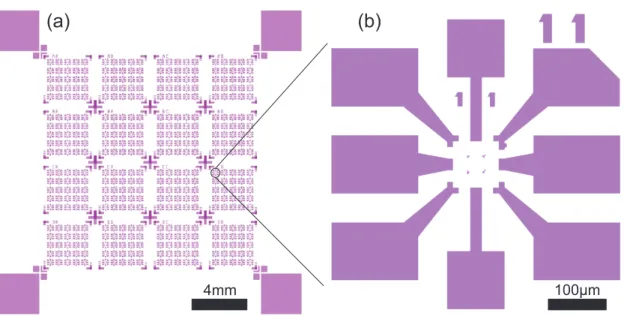
100µm 4mm
Figure 2.2: (a) Optical mask structure to define bond pads, coarse leads and labeling on a 16×16 mm chip. (b) Zoom on a single electrode structure containing eight bond pads.
Afterwards, the chip is placed in hot acetone in order to remove the surplus metal on top of the undeveloped resist.
Then, the fine structures are aligned in the SEM with respect to the coarse ones. In an electron beam lithography (EBL) step, a PMMA resist is exposed by a focused electron beam scanning the defined structures. In this EBL step all the inner parts including the later contacts to the CNT are exposed with overlap to the optically defined structures. Since the nanotube growth starts at a catalyst particle and the nanotubes grow in a non-controllable, arbitrary direction, a circular electrode structure has been designed to increase the probability for an overgrowth process, which is shown in Fig. 2.3. Several electrodes are arranged with varied distances to obtain different suspended segment lengths. Additionally, due to the circular symmetry the suspended length is better defined since the nanotube tends to grow radially outwards. Again the resist is developed and a 40 nm Re layer is deposited with a subsequent lift-off step.
To guarantee freely suspended CNTs bridging two or more contacts the trenches between the circular metal electrodes have to be deepened. This is done by reac- tive ion etching (RIE), where plasma enhanced dry etching anisotropically removes 160 nm of the SiOx while the metal is nearly unaffected and works as etching mask.
At this status all chip structures are defined, namely several contacts with 200 nm deep and 200 nm to 800 nm wide trenches in between, on a single 4×4 mm chip. Fig- ure 2.4 shows an SEM micrograph with tilted stage. Catalyst particles and a CNT
(a) (b)
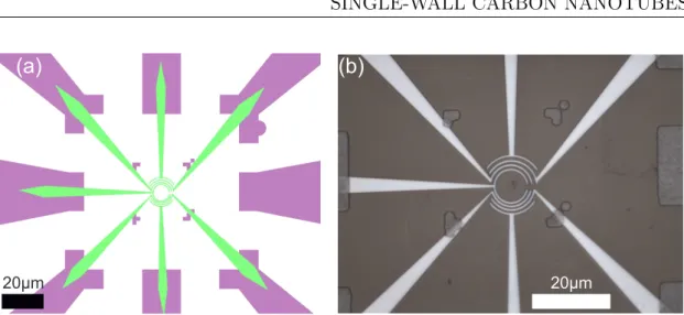
20µm 20µm
Figure 2.3: (a) EBL design for the CNT electrode geometry. (b) Optical microscope picture of circular contact structure aligned to coarse optical mask structures.
are schematically drawn, depicting an ideal situation of a single CNT contacted by several electrodes.
For the CNT growth process a catalyst, composed of transition metal oxide and metalorganic particles suspended in methanol, is needed. The exact composition is listed in Appendix A.4. We use an additional EBL step to place a small amount of catalyst in the center of the circular structures. A drop of the catalyst suspen- sion is cast onto the developed resist and dried on the hot plate to evaporate the methanol. In the following lift-off process the catalyst is removed except for small clusters placed at the structure centers, as illustrated in Fig. 2.4.
The CNT growth process takes place in a quartz tube in an oven heated up to 900◦C while a gas mixture of hydrogen and methane is flowing over the sample. Again, the detailed recipe is listed in Appendix A.5. At the catalyst the methane decomposes and the carbon crystallizes building up the CNT, which grows upwards until it tilts and attaches to the substrate. Van-der-Waals forces fix the CNT at the substrate surface. Despite several attempts in our lab to guide the CNT growth direction us- ing a modified process with a low gas flow rate, in order to obtain laminar flow [Jin et al., 2007], one still observes arbitrary growth directions. Thus the yield of working structures differs in general from sample to sample.
In order to identify the working structures SEM imaging is avoided, since an electron beam focused on a CNT deposits amorphous carbon on the nanotube, as has been shown in Raman spectroscopy. Instead, we solely measure the electric resistance between all electrodes, allowing us to distinguish between contacts connected by a CNT and open- or short-circuited ones. The promising ones are further tested by measuring the back gate dependence of the conductance, and the most auspicious
samples are mounted into the cryostat for low-temperature transport measurements.
SEM pictures as shown in Fig. 2.5 are taken only after all low-temperature transport measurements.
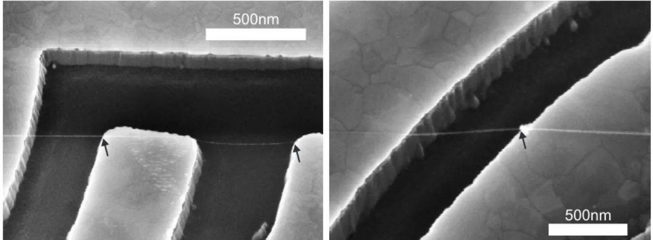
500nm 2µm
300nm 400nm 500nm
200nm nanotube
catalyst
Figure 2.4: Left: Tilted SEM picture of the electrode structure with indicated pos- sible catalyst and CNT position. Right: Zoom on the area marked in the left image with a white rectangle showing the circular electrode geometry in detail.
500nm
500nm
Figure 2.5: Tilted SEM picture of CNTs suspended between rhenium contacts after a successful overgrowth process.
Structure and electronic
properties of carbon nanotubes
Carbon nanotubes are one allotrope of carbon besides graphite (graphene), diamond and fullerenes. This work focuses on single-wall CNTs, which were discovered by Iijima in 1991 [Iijima, 1991] in the products of an arc discharge at graphite elec- trodes by transmission electron microscope imaging. Other fabrication methods include laser evaporation by a pulsed laser beam focused on a graphite substrate and chemical vapor deposition (CVD) [Saito R.; Dresselhaus G, 1998]. Former ex- periments have shown that the last mechanism provides the highest quality in terms of lowest defect density and the highest yield of single-wall CNTs. Additionally, it is compatible with pre-defined on-chip structures, as shown in Chapter 2.
CNTs rapidly became interesting for transport measurements due to their quasi one- dimensionality combined with a perfect regular lattice structure in the ideal case of a clean CNT. At cryogenic temperatures the effectively one-dimensional electronic system1 can be further reduced by tunnel barriers induced by metal contacts, to de- fine quantum dots (QDs), so-called ”artificial atoms”. QDs based on CNTs provide an interesting internal structure, having some degrees of freedom like spin and valley quantum numbers with a pronounced shell configuration. The CNT macro-molecule with its extremely small diameter (≈ 1 nm) provides a highly regular system with relatively high quantum confinement energies among mesoscopic systems.
1For realistic nanotube diameters solely the lowest transversal subband is energetically acces- sible in transport measurements at low temperatures, restricting free propagation only along the nanotube axis.
11
3.1 From graphene to carbon nanotubes
In a first approximation the physical properties of CNTs can be deduced from those of graphene, a one-atom thick layer of carbon atoms arranged in a honeycomb lattice.
This layer, ”rolled up” along the so-called chiral vector C, forms a hollow cylinder~ with a typical diameter of few nanometers. Thus, as a first step we will start with the physics of graphene, later deducing the properties of CNTs.
Graphene is formed by a hexagonal arrangement of carbon atoms, connected by σ-bonds of sp2-hybridized orbitals at 120◦ angles in the plane (see Fig. 3.1(a)).
These orbitals of neighboring atoms overlap forming molecular σ and σ∗ bands, which do not contribute to transport, since they are far away from the Fermi energy.
The remaining pz orbital is aligned perpendicular to the honeycomb plane, forming delocalized bonding π and anti-bondingπ∗ bands.
A B
a1 a2
ac-c
(a) (b)
x y
kx ky
K
K
K K
K
K
b1
b2
Figure 3.1: (a) Graphene lattice in the real space spanned up by the unit vectors
~a1, ~a2. The bond length between the two carbon atoms A, B in the unit cell (shaded gray) is aC–C= 1.42 ˚A. (b) First Brillouin zone of graphene in the reciprocal space with the unit vectors~b1,~b2. The six symmetry points are labeled K and K0.
As depicted in Fig. 3.1, the unit cell of the hexagonal lattice of graphene is spanned by unit vectors
~a1 =
√3 2 a,a
2
!
and ~a2 =
√3 2 a,−a
2
!
. (3.1)
It contains two carbon atoms, labeled A and B in the figure, situated at the positions (0,0) and 13(~a1+~a2) = (a/√
3,0). The lattice constant is a=|~a1|=|~a2|=aC–C·√
3 = 2.46 ˚A, (3.2)
where aC–C = 1.42 ˚A is the carbon atom distance, i.e. the length of the σ-bond. In the reciprocal lattice the corresponding unit vectors~b1,~b2, fulfilling the orthogonality condition~bi·~aj = 2πδij, are
~b1 = 2π
√3a,2π a
!
and ~b2 = 2π
√3a,−2π a
!
. (3.3)
In the tight binding approximation for the delocalizedpz orbitals using Bloch waves, the electronic structure of the valence (π) and conduction (π∗) band of the graphene layer can be calculated. After a further approximation that the overlap integral becomes zero (Slater-Koster scheme) one obtains the simplified dispersion relation of a graphene layer, plotted in Fig. 3.2 (for details see [Saito R.; Dresselhaus G, 1998]):
Egraphene(kx, ky) = ±
"
1 + 4 cos
√3kxa 2
!
cos kya 2
!
+ 4 cos2 kya 2
!#1/2
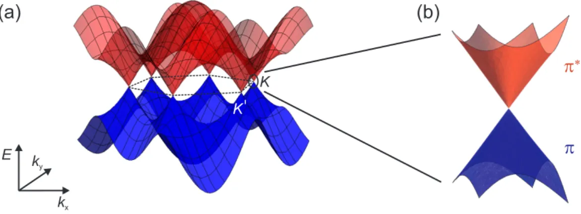
. (3.4) Due to the twoπ electrons per unit cell the lowerπ band is fully occupied, while the π∗ band is empty. However, the most remarkable electronic property of graphene is the ”zero-energy band gap” at the six corners of the Brillouin, the so-called K- points. Only two are independent, labeled K, K0, while the others are connected by reciprocal lattice vectors. In the low energy limit the dispersion at this K-points is linear, as can be seen in the zoom in Fig. 3.2(b). Due to these features of the dispersion relation graphene exhibits quasi-metallic behavior.
(a) (b)
kx ky
E
K K
Figure 3.2: (a) Energy dispersion of theπand π∗ bands in graphene calculated with Eq. 3.4. (b) Detail view of one so-called Dirac cone, which are located at theK and K0 points in the Brillouin zone. Here the valence (π) and conduction (π∗) bands touch and the dispersion relation is linear.
There is a large amount of possibilities how a CNT can be formed from a graphene sheet. The chiral vector C~ =n ~a1 +m~a2 ≡(n, m), along which a CNT is rolled up, uniquely characterizes each of these possibilities. By definition, owing to the hexag- onal symmetry, the range 0 ≤ |m| ≤ n for the parameters m, n is sufficient. The length of the chiral vector|C|~ =a√
n2+m2+nm corresponds to the circumference of the nanotube.
A B a1 a2
C = (6,4)
T = (7,-8)
(6,4)
(a) (b)
Figure 3.3: (a) Schematic drawing of the graphene lattice. The blue arrows define the unit cell of a (6,4) CNT, spanned by the chiral vector C~ and the perpendicular vectorT~. (b) Sketch of a rolled-up (6,4) nanotube segment generated withNanotube Modeler ( c JCrystalSoft, 2013).
The angle between the chiral vectorC~ and a~1 is called chiral angleθ. It is restricted to the range 0≤ |θ| ≤ 30◦ due to the hexagonal symmetry of the graphene lattice.
This chiral angle θ can be expressed in terms of the chiral indices as cos(θ) = C~·a~1
|C||~ a~1| = 2n+m 2√
n2+m2 +nm. (3.5)
In particular, zigzag and armchair nanotubes correspond to θ = 0◦ (m = 0) and θ = 30◦ (m=n), respectively.
To define a carbon nanotube unit cell one also needs a vector that gives the period- icity of the CNT in direction of its axis – the so-called translation vector
T~ =t1~a1+t2~a2, (3.6) with integers t1 and t2, which can be expressed by
t1 = 2m+n
dR and t2 =−2n+m
dR , (3.7)
where dR is the greatest common divisor of (2m+n) and (2n+m).
With the unit cell of a nanotube, spanned by C~ and T~, the structure of the nan- otube is unambiguously defined. As an example, Fig. 3.3 shows the unit cell of a (n, m) = (6,4) CNT, with dR= 2, t1 = 7 andt2 =−8.
”Rolling up” a graphene sheet has consequences for the electronic structure of the resulting single-wall carbon nanotube (SWCNT). A novel boundary condition is in- troduced. Due to the finite circumference of the CNT the wave vector inC~ direction k⊥ becomes quantized, while the longitudinal wave vector inT~ directionkk remains continuous as long as one assumes infinitely long nanotubes.
Due to this boundary condition (the phase of the wave function has to be identi- cal modulo 2π after one circulation) the energy dispersion relation of each band of graphene (π, π∗) collapses into one-dimensional parallel subbands, also called transversal modes, with spacing
∆k⊥ = 2π
C~. (3.8)
Thus only discrete wave vectors along theC-direction are allowed, while a continuous~ dispersion in the nanotube axis direction, along T~, remains. Restricting to one subband the Brillouin zone becomes one-dimensional. The one-dimensional band structure of a (n, m) nanotube is given by the zone-folding relation deduced from the two-dimensional band structure of graphene:
E(kk, µ) =Egraphene
k K~2
|K~2| +µ ~K1
. (3.9)
Here kk is the longitudinal wave vector (−π/T < kk < π/T; T = |T~| is the translation period of the nanotube in Eq. 3.6) and µ is a discrete quantum number (µ= 1,2, ..., N where N is the number of carbon pairs in the unit cell of the nano- tube). An example for the collapse of the dispersion is shown in the Fig. 3.4.
The vectors K~1 and K~2 are expressed by the reciprocal lattice vectors b~1 and b~2 of the graphene sheet as
K~1 = −t2~b1+t1~b2
N and K~2 = m~b1−n~b2
N . (3.10)
If aK-point, where the valence and the conduction band of graphene are degenerate, fulfills the boundary condition, the CNT is metallic. A metallic behavior can for instance be found in the case of a (3,3) CNT in Fig. 3.4 where the line cuts intersect the K-points. Otherwise, for low energies it has approximately parabolic bands separated by an energy gap, and the nanotube displays semiconducting behavior.
(a) (b)
/a 0 /a
K K‘
energy
EF
ky kx
k
k
Figure 3.4: (a) Rolling up the CNT leads to a restriction of allowed wave vectors.
The case of a (3,3) CNT is indicated as blue lines on top of the graphene dispersion gray scale plot. (b) The corresponding energy dispersion for the one-dimensional subband of a (3,3) CNT shows a degeneracy at the K and K0 point. This causes metallic behavior.
This behavior can be traced even by room temperature transport measurements where nanotubes are electrically contacted on a substrate and capacitively coupled to a gate. Applying a voltage to the gate changes the chemical potential of the electrons in the nanotube shifting them with respect to the Fermi energy of the leads. Figure 3.5 displays a sketch of the resulting typical dependence of the conductance on the gate voltage at room temperature. In the case of a metallic nanotube (Fig. 3.5(a)) the conductance does not depend on the back gate voltage, since no band gap exists:
one CNT subband intersects the K or K0 Dirac point. The condition for metallic conduction can be derived from Eq. 3.8. One obtains for the chirality (n, m) the condition
n−m = 3q, (3.11)
where q is an integer number. As a consequence, following this model, statistically one third of the single-wall carbon nanotubes are metallic, two third are semicon- ducting. For semiconducting CNTs, the conductance drops to zero in the band gap (Fig. 3.5(c)).
This zone-folding approximation neglects curvature effects like changing bond lengths and not perfectly parallel pz- orbitals. Taking the curvature into consideration, only armchair nanotubes (n=m) remain really metallic, the other ones fulfilling Eq. 3.11 develop a small band gap Eg leading to a dip in G(Vg) at room temperature as de- picted in Fig. 3.5(b), sinceEg 'kBT. For more details see [Charlier et al., 2007]. A further effect of the curvature is the induced spin-orbit coupling in CNT, which is almost absent near Dirac points in graphene [Huertas-Hernando et al., 2006]. The
2 G (e/h)
Vg (V)
0 Vg (V) Vg (V)
(a) (b) (c)
2 G (e/h) 2 G (e/h)
0 0
Figure 3.5: Sketches of conductance tracesG(Vg) at room temperature for (a) metal- lic (b) small-bandgap and (c) semiconducting CNTs. The insets depict the lowest subbands for the respective type of CNT. These are shifted by the gate voltage Vg
with respect to the electro-chemical potential of the leads (red line).
spin-orbit coupling can be revealed by transport spectroscopy, as e.g. demonstrated in the Chapters 5.1 and 5.2.
3.2 Electronical properties of carbon nanotube quantum dots
The one-dimensional CNT band structure can be further reduced by forming a so- called quantum dot (QD) [Tans et al., 1997], a conducting island separated from leads by tunnel barriers.
Different methods exist to create QDs, e.g. self-assembled metal clusters, lateral QDs which are electro-statically defined in two-dimensional electron gases (2DEG), or contacted nanowires. In this work, the quantum dot is defined in the suspended part of a carbon nanotube at low temperatures. In the following the relevant QD theory is deduced starting with a metallic island, which forms a classical single electron transistor, where the number of charges is quantized. Reducing the charge carrier density leads to an increase of the size quantization induced energy spacing giving rise to quantum Coulomb blockade.
A survey of the different transport regimes is given in the Table 3.1.
3.2.1 From classical to quantum Coulomb blockade
We assume an electrically isolated conductor, which is connected to leads by tunnel barriers. In Fig. 3.6(a) a replacement circuit is depicted. For electronical transport measurements the QD has to be coupled to source (S) and drain (D) leads enabling
(a) ∆.e2/CΣ kBT no discreteness of charge due to:
• temperature to high
• quantum dot not small enough
• tunneling resistance too low
(b) ∆kBT e2/CΣ classical or metallic Coulomb blockade regime:
• many levels contribute to tunneling
• many levels excited by thermal fluctuations (c) kBT ∆ < e2/CΣ quantum Coulomb blockade regime:
~ΓkBT • only one or a few levels participate in transport
• width of conductance peaks set by temperature Table 3.1: Transport regimes for a conducting island coupled to leads.
the modification of the QD charging state. The coupling is provided by tunnel barriers between leads and QD with tunnel rates ΓS,ΓD, which can be modeled as resistors parallel to capacitors CS, CD. In order to modify the electro-chemical potential of the electrons on the island a gate voltage can be applied to a nearby gate electrode (G), which is capacitively coupled to the quantum dot (QD) via the capacitance Cg.
Depending on the relevant energy scales one has access to different transport regimes.
As long as the thermal energy is dominating the tunnel barriers will not be effective and the transport through the conducting island will behave in a classical way, the charge quantization will not be noticed. This case is listed in (a) of the Table 3.1.
To obtain charge quantization on the island its size has to decrease leading to a low capacitance. As consequence, the electrostatic charging energy EC = e2/2CΣ will reach values of some tens of meV exceeding the thermal energy Eth = kBT at low temperatures, i.e. kBT EC = e2/2CΣ. Here CΣ is the total capacitance of the conducting island. In a setup as illustrated in Fig. 3.6(a), the total capacitance is given by the sum of gate Cg, source CS, and drain CD capacitance plus parasitic ones: CΣ =Cg+CS+CD+Cenv. The consequence is an electrostatic suppression of the current due to Coulomb interaction which is called Coulomb blockade. Here, the Coulomb repulsion prevents an additional electron from tunneling onto the QD.
A further requirement for the occurrence of Coulomb blockade is that the tunnel resistances from the source and drain lead RS,D to the dot must be bigger than the quantum resistanceRS,D RK'25.8 kΩ in order to suppress quantum fluctuations of the charge on the island. If these conditions are fulfilled the current through the island is blocked by the Coulomb repulsion and the charge on the dot is fixed, as has been first observed in metallic islands [Grabert et al., 1993], [Ralph et al., 1995].
D
CD
S
CS
S D
G Cg
QD (a)
µN µN+1
µN-1
(b)
E
Cenv E
Figure 3.6: (a) Replacement circuit of a quantum dot coupled to a source (S) and a drain (D) contact by tunnel barriers with tunnel rates ΓS,Dand capacitancesCS,D. A gate (G) is capacitively coupled to the QD to change the electro-chemical potential of the QD states. (b) Discrete ”charging levels” in a classical QD with equidistant level spacing ∆E =EC =e2/2C given by the classical charging energy.
Due to the small Fermi wavelength in metallic islands the energy level separation ∆ is usually much smaller than the charging and thermal energy, i.e. ∆kBT EC, and can be neglected. The charging energy is assumed to be independent of the charging state and thus the energy required to put an additional electron on the dot is constant. This is indicated in Fig. 3.6(b) showing the ”charging levels” which are equally spaced by the charging energy ∆E =EC.
The conditions for this classical Coulomb blockade, as summarized in Table 3.1(b), can be technologically met nowadays in terms of micro- and nano-fabrication and by dilution cryostats with temperatures down to T '10 mK.
If the density of statesns of the QD is low, as e.g. in two-dimensional semiconduc- tors, the Fermi wavelength λF can reach values around 50 nm, since λF =q2π/ns [Beenakker, 1991], [Kouwenhoven et al., 1997], and the quantum mechanical quan- tization energy ∆ can attain the same order of magnitude as the charging energy (see Table 3.1(c)). Then the energy differences ∆E are not equal anymore but now consist of both the classical charging energy EC, which is constant within the so- called constant interaction model [Glazman and Shekhter, 1989], [McEuen et al., 1991], plus the single-particle level spacing ∆, which is required to reach the next unoccupied quantum level. The latter one originates from the quantum mechanical size quantization in all three dimensions and is in general dependent on the charging state. Further details of the QD physics can be found in [Kouwenhoven et al., 1997].
In the simplest model assuming twofold spin-degenerate states and neglecting any exchange interactions, one expects a finite ∆only for every second electron induc-
ing a transition of the spin quantum numberS = 0→1/2. This is the case ofSU(2) symmetry.
In the special case of CNTs, besides the spin degeneracy additionally theKK0 valley degree of freedom has to be taken into account, which originates from the underly- ing graphene lattice. For the highly symmetric case the QD levels in CNTs are thus fourfold both spin and valley degenerate, as has been seen in experiments [Liang et al., 2002], [Sapmaz et al., 2005]. As shown in Fig. 3.7, the longitudinal quantiza- tion leads to spin-degenerate levels equidistant inkkdirection for both valleys. If the levels are symmetric in the different valleys (K,K0), the respective levels are energet- ically equal leading to fourfold degeneracy. Hole and electron states are separated by the band gap Eg.
K K‘
(a) (b)
Eg
E
k
Eg
K K‘
Figure 3.7: (a) Lowest transversal subbands of K and K0 valley for a maximum degenerate (∆SO = ∆KK’ = 0) semiconducting CNT with indicated quantum dot levels caused by the longitudinal quantization of the one-dimensional nanotube. (b) Energy level diagram in an exemplary CNT QD with spin- and valley- degenerate longitudinal modes, indicated by the spin-up and spin-down arrows for the K and K0valley. The separation of hole and electron levels is given by the band gap sizeEg and ∆ represents the ”quantum energy”. Note that the diagram does not include the electrostatic charging energy which has to be paid for each additional electron on the QD.
3.2.2 Influence of spin-orbit coupling, KK
0-mixing, and mag- netic fields on the quantum dot levels
In the following, based on theSU(4) symmetry, as discussed above, we will now also take into account symmetry breaking. The CNT levels are modeled without any electron-electron interactions, assuming only one electron occupying a longitudinal mode.
It is sufficient in a good approximation to use a minimal Hamiltonian for a single longitudinal mode of a CNT-QD. Including spin-orbit coupling, KK0-mixing and a magnetic field forming an angle ϕ with the nanotube axis. Then, the Hamiltonian reads
HˆCNT =εdIˆσ⊗Iˆτ+ ∆KK’
2 Iˆσ⊗τˆz+ ∆SO
2 σˆz⊗τˆx+ + 1
2gsµB|B|~ (cosϕσˆz+ sinϕσˆx)⊗Iˆτ +gorbµB|B~|cosϕIˆσ ⊗ˆτx.
(3.12)
The basis is formed by the states{|a↑i,|b ↑i,|a ↓i,|b ↓i}, where
|ai= |Ki+|K0i
√2 , |bi= −|Ki+|K0i
√2 (3.13)
are the anti-bonding and bonding combination of the different valley eigenstates|Ki and|K0i, respectively. The operators ˆτi and ˆσi (i=x, y, z) act in the valley and spin spaces, respectively, such that|ai,|biare the eigenstates of ˆτz, while| ↑i,| ↓iare the eigenstates of ˆσz. Spin-orbit interaction splits the fourfold degeneracy, forming two Kramers doublets at B = 0 with energy spacing ∆SO. These are further hybridized by the valley mixing, which is typically referred to disorder but can also be induced by the axial boundary conditions. The pure valley and spin states are restored in the high field range gsµB|B~| ∆SO,∆KK’.
The first term in the Hamiltonian 3.12 gives the reference energyεdof the considered longitudinal mode, the second term takes into account the valley mixing with the corresponding energy ∆KK’. The last term in the first line incorporates the spin- orbit interaction energy ∆SO. In the second line the effect of a magnetic field is included, where the first term stands for the Zeeman effect, while the last one takes into account the Aharonov-Bohm effect caused by the cylindrical topology of the CNT and the parallel component of the field.
The magnetic field dependence of the eigenstates both in perpendicular (φ = π/2) and parallel (φ= 0) orientation to the nanotube axis are obtained by the diagonal- ization of the Hamiltonian 3.12 and is shown in Fig. 3.8 for different values of the parameters ∆SO and ∆KK’. In this figure, the behavior of the states in a magnetic field is plotted for perpendicular orientation of the magnetic field to the CNT axis
on the left side, and for parallel orientation on the right side.
In the zero field case with ∆SO = ∆KK’ = 0, Fig. 3.8(a), the quantum state is four times degenerate. In finite field the levels split linearly according to their magnetic moment. The orbital magnetic momentgorbµB depends on the CNT diameter and is typically bigger than the spin magnetic momentgsµB. In Fig. 3.8 the orbitalg-factor is set to twice the spin g-factor resulting in steeper slopes of the state with parallel aligned spin and orbital magnetic moment in the parallel magnetic field. While in the perpendicular case only the Zeeman splitting of valley degenerate states occurs, in the parallel orientation also the orbital momentum couples to the field with an overlying Zeeman splitting.
For finite spin-orbit coupling ∆SO >0, depicted in Fig. 3.8(b), the quadruplet splits at B = 0 into so-called Kramers doublets with energy spacing ∆SO. As a conse- quence of the spin-orbit coupling the spin perpendicular to the nanotube is not a good quantum number anymore, since the spin aligns with the orbital moment in the direction of the nanotube axis. In parallel field the different slopes of the states show the distinct ways to couple spin and the valley quantum numbers K, K0. In Fig. 3.8(c) the finite KK0-mixing leads again to a splitting into doublets at zero field with spacing ∆KK’. The situation becomes even more complicated in 3.8(d) for both finite ∆KK’ and ∆SO, where the doublet spacing ∆ at zero field is a function of both energies, ∆ =
q
∆KK’2+ ∆SO2. Additionally, in both field orientations an anti- crossing mixes the states. This case will be discussed in more detail in Chapter 5.1 and 5.2.