Nanomechanical Instability and Electron Interference Blockade in Carbon Nanotube Quantum Dots
Dissertation
zur Erlangung des Doktorgrades der Naturwissenschaften (Dr. rer. nat.)
der Fakultät für Physik der Universität Regensburg
vorgelegt von Michael Schafberger
aus Regensburg
im Jahr 2018
Die Arbeit wurde von Prof. Dr. Christoph Strunk angeleitet.
Das Promotionsgesuch wurde am 23.01.2018 eingereicht.
DasPromotionskolloquium fand am 09.11.2018 statt.
Prüfungsausschuss: Vorsitzender: Prof. Dr. Gunnar Bali 1. Gutachter: Prof. Dr. Christoph Strunk 2. Gutachter: PD. Dr. Andrea Donarini weiterer Prüfer: Prof. Dr. John Lupton
Contents
Contents iii
1 Introduction 1
2 Theoretical Background 3
2.1 Properties of Carbon Nanotubes . . . 3
2.1.1 Atomic Structure . . . 3
2.1.2 Electronic Band Structure . . . 5
2.2 Electronic Transport in Carbon Nanotubes . . . 8
2.2.1 Ballistic Transport . . . 9
2.2.2 Classical Transport . . . 10
2.2.3 Diffusive Transport . . . 10
2.3 Quantum Dots and Coulomb Blockade . . . 11
2.3.1 Coulomb Blockade at Zero Bias . . . 11
2.3.2 Quantum Coulomb Blockade . . . 14
2.3.3 Coulomb Blockade at Finite Bias . . . 15
2.3.4 Carbon Nanotube Quantum Dots . . . 18
2.4 Coherent Population Trapping . . . 20
2.4.1 Coherent Population Trapping in Optics . . . 20
2.4.2 All Electronic Coherent Population Trapping . . . 23
2.4.3 Coherent Population Trapping in Carbon Nanotubes . . . . 24
2.5 Noise . . . 30
2.5.1 Noise Sources . . . 31
2.5.2 Noise Measurement Techniques . . . 33
2.6 Nanoelectromechanical Properties of CNTs . . . 36
2.6.1 Mechanical Vibrations in Suspended Carbon Nanotubes . . 36
2.6.2 Effects of Vibration Modes on Electronic Transport . . . 39
3 Sample Fabrication and Experimental Setup 45 3.1 Sample Fabrication . . . 45
iii
3.1.1 Substrate . . . 45
3.1.2 Lithography and Metalization . . . 46
3.1.3 CNT Growth . . . 46
3.2 Experimental Setup . . . 47
3.2.1 Cryogenics . . . 47
3.2.2 Noise and Transport Measurement Setup . . . 48
3.2.3 Noise System Calibration . . . 51
3.2.4 Measurement Routine . . . 53
4 Dark States in Carbon Nanotube Quantum Dots 57 4.1 Basic Sample Characterization . . . 57
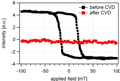
4.1.1 Contact Material . . . 57
4.1.2 Electronic Sample Characterization . . . 59
4.2 Dark States . . . 63
4.3 Numerical Comparison . . . 67
4.4 Chapter Summary . . . 71
5 Electromechanical Instabilities 73 5.1 Basic Device Characterization . . . 73
5.2 Instabilities . . . 79
5.3 Magnetic Field Dependence . . . 84
5.4 Noise Measurements . . . 87
5.5 Chapter Summary . . . 93
6 Summary and Outlook 95 A Recipes 97 A.1 Contact Fabrication . . . 97
A.2 CNT synthesis . . . 99
A.2.1 Catalyst dots . . . 99
A.2.2 CVD growth . . . 100
Bibliography 103
Acknowledgement 117
1
Introduction
Single walled carbon nanotubes were first observed in arc-discharge experiments [1,2] and first measurements of single nanotubes contacted with metallic contacts were performed in 1997 [3, 4]. The ongoing improvement in nano-fabrication techniques opened more possibilities for a large variety of measurements. Since carbon nanotubes are intrinsic one-dimensional conductors, the formation of a quantum dot system is straightforward in comparison to two-dimensional elec- tron gas systems, where the quantum dot has to be constricted electrostatically.
Many different transport behaviors were observed in carbon nanotube systems, e.g. Luttinger-liquid behavior [5, 6], ballistic transport [7] and Fabry-Pérot-like oscillations [8]. Adding the possibility of contacting the carbon nanotubes with different types of metallic leads, including ferromagnetic [9] and superconduct- ing materials [10, 11] a lot of research can be performed on such systems.
Having the possibility of performing Shot noise measurements on these systems, a powerful tool to gain a deeper understanding of the underlying processes is at hand [12–14].
In addition, carbon nanotubes have excellent mechanical properties, e.g. a low mass, high stiffness and a huge Young’s modulus [15]. They can act as mechani- cal beam resonators with high quality factors of the bending mode [16, 17]. This allows to employ carbon nanotubes as ultra-sensitive mass sensors [18] and is also a promising system to reach the quantum limit of mechanical motion.
Also from a technological point of view carbon nanotubes represent a promis- ing material system. With the downscaling of transistors in the semiconductor industry reaching its limits [19], Moore’s Law [20], which says that the number of transistors in an integrated circuit doubles every two years, will come to an end. Switching from silicon to CNT-based transistors might be the solution to further increase the number of devices in integrated circuits, since no isolation region between the n-type and p-type field effect transistors (FETs) is necessary in CNT CMOS circuits [21]. Apart from replacing active devices, CNTs might also replace on-chip interconnect applications due to their ability to carry high
1
current densities with a fixed resistance over several micrometers [22].
In this thesis the effect of electron interference and nanomechanical instabilities on the transport behavior of carbon nanotube quantum dots is investigated. It is organized as follows: Chapter 2 gives a background on the theory necessary for this thesis. At first the atomic and electric properties of carbon nanotubes, as well as their transport behavior is presented. Then the basics of quantum dots, Coulomb blockade and especially carbon nanotube quantum dots are explained.
The next section deals with the effect of charge population trapping in general, in quantum dot systems and in the special case of dark states in carbon nanotube quantum dots due to electron interference. Then different sources of noise and noise measurement techniques are presented. The last section of chapter 2 deals with the nanomechanical properties of suspended carbon nanotubes, the differ- ent vibrational modes and their effects on the electronic transport. In chapter 3 the sample fabrication method and the experimental setup, as well as the cali- bration of the noise measurement setup is presented. Chapter 4 shows the effect of electron interference in a clean and regular carbon nanotube quantum dot. At first, a basic sample characterization is performed, before the transport features of dark states are examined in detail. These are then compared to the theoret- ical model by numerical simulations. In chapter 5 the influences of nanome- chanical motion of a suspended carbon nanotube quantum dot on the electronic transport is presented. After a basic sample characterization, instabilities inside charge transitions and extensions of conducting regions, caused by nanomechan- ical feedback, are investigated. The magnetic field dependence of these features, as well as their signature in noise measurements are shown. After a general dis- cussion and outlook in chapter 6 the recipes for all fabrication steps are listed in the appendix.
2
Theoretical Background
This chapter provides the theoretical background needed for the interpretation of the experimental results presented in this work.
First the structural, electronic and transport characteristics of carbon nanotubes are shown. The basic principles of Coulomb blockade, quantum dots in general as well as the special case of carbon nanotubes are introduced. Then the effect of coherent population trapping in atomic physics is introduced. This concept is then transfered to quantum dot systems and its realization in a single carbon nanotube quantum dot is explained. An overview of the different sources of noise and noise measurement setups is given. At last the different vibrational modes of suspended carbon nanotubes and their effect on the electronic transport is discussed.
2.1 Properties of Carbon Nanotubes
The following section summarizes the general properties of carbon nanotubes.
The atomic structure, the electronic properties and the mechanisms of electronic transport in this material system are presented, following the references [23–26].
2.1.1 Atomic Structure
In nature carbon has different allotropes such as diamond, graphite, graphene, fullerenes or carbon nanotubes. However there are only two variations of valence bonds between the carbon atoms. In one case, ones-orbital and threep-orbitals form foursp3-orbitals through hybridization. This results in a tetrahedral unit, which forms the three dimensional structure of diamond. The other case is the sp2 hybridization, formed by ones-orbital and two p-orbitals, which results in a planar hexagonal lattice. This one-atom thick layer is called graphene, which was first experimentally isolated in 2004 [27] and has become increasingly important since.
3
Carbon nanotubes (CNTs) can be described as a graphene sheet rolled up into a cylinder. If they consist of only one layer of graphene, one speaks about single walled carbon nanotubes (SWCNTs). Their wall thickness therefore is only one carbon atom. A coaxial arrangement of multiple tubes inside each other is called multi walled carbon nanotube (MWCNT). They were first observed in 1991 by S.
Iijama [1] via tunneling electron microscopy.
CNTs can be fabricated by different methods such as arc discharge, laser ablation, high pressure CO conversion (HiPCO) and chemical vapor deposition (CVD) [28].
The latter approach was used in this work and is explained in Ch. 3.1.3, with its exact recipe presented in App. A.2.2.
a b c
(6,6) (9,0) (9,2)
Figure 2.1: Carbon nanotubes with different chiral angles: a Armchair CNT, b zigzag CNT,cchiral CNT. Created withNanotube Modeler 1.7.8.(©JCrystalSoft 2015)
A single walled carbon nanotube is obtained by rolling up a graphene sheet along the chiral vectorC~ which is defined via the lattice vectors of graphene~a1 and~a2
C~ =m·~a1+n·~a1→(n, m). (2.1) The chiral indices m and n define the structure of a SWCNT. The tilt angle be- tween the hexagon structure and the nanotube axis, or between~a1andC~, is called chiral angleΘand is also defined by the chiral indices
Θ= arccos 2n+m 2
√
n2+m2+nm
!
. (2.2)
2.1. PROPERTIES OF CARBON NANOTUBES 5 Due to the hexagonal symmetry of the honeycomb lattice the chiral angleΘis in the range of 0°≤ |Θ| ≤30°. Depending onΘ one can distinguish three different types of SWCNTs: Zig-zagCNTs, where (n,m) = (n,0) andΘ = 0°, form a zig-zag pattern along the circumference, highlighted with a red line in Fig. 2.1a.
Armchairtubes have the conditions (n,m) = (n,n) andΘ = 30° and show an arm- chair pattern along the circumference, shown in Fig. 2.1b. The remainingchiral tubes with (n,m,n,0) and 0°≤ |Θ| ≤30° feature no distinct pattern at the cir- cumference. One example of a chiral tube with the chiral indices (9,2) is shown in Fig. 2.1c.
The diameter of a CNT dt also depends on the chiral indices and is given by dt=
C~ π
= a π
√
n2+m2+nm, (2.3)
where a = 1.42 Å·
√ 3.
The unit cell of a carbon nanotube is the rectangleOABB´, depicted in Fig. 2.2, which is spanned by the vectorsC~ andT~. The number of hexagons per unit cell Nis defined by
N= |C~×T~|
|~a1×~a2|. (2.4)
Since each graphene unit cell consists of two atoms, the number of carbon atoms in one CNT unit cell is2N.
2.1.2 Electronic Band Structure
Just as the atomic structure of CNTs originates from that of graphene, many prop- erties of the electronic band structure can also be deduced from graphene.
The graphene unit cell contains two atoms with three sp2-orbitals and one pz- orbital each. Thesp2-orbitals overlap with those of the neighboring atoms, form- ing a bonding bandσ and an antibonding bandσ∗. These bands do not partici- pate in transport, since they are far away from the Fermi level. Thepz-orbitals, which are perpendicular to the honeycomb plane, get delocalized and form bond- ing and antibonding bands calledπandπ∗.
In Fig. 2.3a a primitive unit cell of graphene is depicted. It is spanned by the two base vectors ~a1 and ~a2 and contains two carbon atomsA and B. In the re- ciprocal space the Brillouin zone of the unit cell of graphene is again hexagonal, as depicted in Fig. 2.3b. The corners are alternately labeled K and K’. Since the three K (K’) points are connectable by reciprocal lattice vectors, they therefore
Figure 2.2: Honeycomb lattice of graphene. Surface area of the nanotube is defined by the chiral vectorC~ and the translational vectorT~. The blue (red) arrows indicate the base vectors~a1 (~a2) of graphene. The chiral angleΘ is defined as the tilt angle between the nanotube axis and the underlying hexagon structure.
a b
Figure 2.3:aHoneycomb lattice in real space. The blue area shows a primitive unit cell containing two atomsAandB. The unit cell is spanned by the two base vectors~a1and
~a2. bLattice of graphene in~k-space. The blue hexagon is the first Brillouin zone and~b1 and~b2are the corresponding reciprocal lattice vectors.
2.1. PROPERTIES OF CARBON NANOTUBES 7 correspond to equivalent electron states.
In the tight binding approximation the valence (π) and conduction (π∗) band of graphene can be calculated from thepz-orbitals of carbon and the simplified dis- persion relation can be expressed as
E(kx, ky) =±γ0
"
1 + 4 cos
√ 3kxa
2
!
cos kya 2
!
+ 4 cos2 kya 2
!#1/2
, (2.5) whereγ0≈3 eV is the hopping energy between the carbon atoms.
Following Eq. 2.5 the energy dispersion has no bandgap, since the π and π∗ bands touch at K and K’, where the density of states is zero. This makes un- doped graphene a semimetal.
In a first approximation the graphene band structure stays unperturbed by rolling up into a CNT, except for adding a periodic boundary condition in the circum- ferential direction. This so called "zone-folding approximation" leads to a quan- tization of the wave vector component perpendicular to the chiral vectorC:~
k⊥=~k·C~ = 2πq, (2.6)
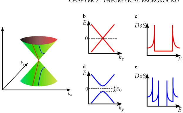
where q is an integer. The parallel component of the wave vector stays contin- uous, since the length of the CNT is assumed infinite. The allowed values of~k lead to lines in reciprocal space at an angle π/3 +Θ from the kx axis, with the distance between two lines being inversely proportional to the CNT diameter, i.e.∆k= 2/d. Since the one-dimensional dispersion relation is a cut of the two- dimensional dispersion relation of graphene along the quantization lines, the chi- ral vectorC~ and chiral angleΘ and therefore the chiral indices (n,m) determine whether a CNT is metallic or semiconducting. In graphene the dispersion rela- tion is linear close to the Fermi surface, which results in a cone-like shape around the Dirac points (K,K’), as depicted in Fig. 2.4a. Since the closest branch to the Fermi level determines the transport behavior, the other cuts can be neglected.
Figure 2.4b shows the resulting energy dispersion if a cut runs through a Dirac point. There is no band gap and the corresponding density of states, which is plotted in Fig. 2.4c, is always greater than zero. Therefore the carbon nanotube is metallic. The situation in which there is a separation|∆κ⊥|between the cut and the Dirac point is shown in Fig. 2.4d and e. The dispersion relation results in two hyperbolic bands with a gapEG= 2~vF|∆κ⊥|, wherevF= 8×10⁵ms−1is the Fermi velocity. The density of states becomes zero inside the bandgap and the CNT is semiconducting. It can be shown that only when the chiral indices are such that (n-m)/3∈Zthe resulting nanotube is metallic.
a b c
d e
Figure 2.4: a Dispersion relation of graphene at low energies results in Dirac cones.
Quantizedkxvalues lead to cuts through the graphene dispersion.bIf a cut goes through a K point (red line), the CNT dispersion is linear, there is no bandgap and the tube is metallic.cThe density of states is then constant.dIf a cut misses the K point (blue line), the resulting CNT dispersion relation shows a bandgap. eThe tube is semiconducting and the density of states goes to zero within the gap.
2.2 Electronic Transport in Carbon Nanotubes
Considering an electric current through a wire, the conductanceGand the resis- tanceRare given byG=σ A/Land R=ρL/A=G−1, whereL is the length of the conductor andAits cross sectional area. If the conductor is macroscopic, the con- ductivityσ and the resistivityρ= 1/σ are material constants and independent of the lengthLand areaA. When the size of the conductor becomes small compared to the characteristic lengths for the electron motion,σ andρwill depend on the length and area of the conductor due to quantum effects like interference caused by scattering on boundaries, defects or impurities.
There are at least three characteristic lengths which have to be considered in mesoscopic systems: The Fermi wavelengthλF, the mean free pathLm and the phase relaxation lengthLφ. The Fermi wavelengthλF = 2π/kF is the de Broglie wavelength for electrons at the Fermi energy. The mean free path Lm, or mo- mentum relaxation length, is the average distance an electron travels before it is
2.2. ELECTRONIC TRANSPORT IN CARBON NANOTUBES 9 scattered, and the phase relaxation lengthLφis the length over which an electron retains its phase information.
The different scattering mechanisms do not affect these length scales equally. For instance, elastic scattering only contributes toLm and not Lφ, whereas inelastic scattering influences both. The scattering between two electrons does not affect Lm, but onlyLφ. Since only electrons near the Fermi energy contribute in trans- port experiments, time scales for the phase relaxation length and the mean free path can be determined via the Fermi velocity, e.g. the momentum relaxation timetm=Lm/vF and the phase relaxation timetφ =Lφ/vF. The relation between the length scales determines three different transport regimes: ballistic, diffusive and classic transport. These regimes will be discussed in this section.
2.2.1 Ballistic Transport
For ballistic transport the relationLLm, Lφ is valid and leads to conduction of single electrons with no phase and momentum relaxation. This can be described by the Landauer-Büttiker formalism [29]. The current for one conduction chan- nel is given by
I = e h
Z
d(fL()−fR())T(), (2.7)
whereT() is the transmission probability and fL,R(E) is the Fermi Dirac distri- bution for the two contacts:
fL,R(E) = 1
1 +e(E−µL,R)/kBT . (2.8) For zero temperature the conductance of this system is
G(0) =e2
hT(0). (2.9)
This leads to a maximum conductance Gmax =e2/h for a mesoscopic conductor in the ballistic transport regime with full transmission (T = 1). Due to the spin and valley degeneracy in carbon nanotubes, there are four conductance channels available. Therefore the maximum conductance in CNTs increases to
Gmax= 4e2
h, (2.10)
which leads to a minimal resistance of
Rmin = 1/Gmax≈6.4 kΩ. (2.11)
Due to impurities in the carbon nanotube, the conductance in real samples is reduced to G <4e2/h. Examples of ballistic transport in CNTs, where the tube between the contacts acts as a Fabry-Pérot interferometer, can be found in Ref.
[8, 30].
2.2.2 Classical Transport
For Lφ Lm L phase and momentum relaxation events occur so often that the electron wave function cannot be described by a single phase and therefore the Schrödinger’s equation cannot be solved for the entire sample. In this case the total resistance consists of a series connection of microscopic resistances for every momentum relaxation lengthLm. Summing up all resistances simply gives Ohm’s law as expected for a classical conductor.
2.2.3 Di ff usive Transport
ForLm Lφ < L many elastic scattering events take place. They only affect the mean free pathLm. Therefore the conductor is in the diffusive transport regime and the wave function becomes localized. There are two different cases of local- ization, which are discriminated by the localization lengthLC =MLm, whereM is the number of conduction channels. If the phase coherence lengthLφ is larger than the localization length LC, the system is in the strong localization regime, where the conductance arises from thermal hopping from one localized state to another. If the localization length is larger than the phase relaxation length, the sample is in the weak localization regime, where universal conductance fluctu- ations and negative magnetoresistance can be observed. The interaction of elec- trons with each other has only a small effect on macroscopic systems, since the long range part of the Coulomb interaction is screened. However for conductors of reduced dimensions, the Coulomb interaction is not effectively screened and the electron-electron interaction becomes important. One implication of that is Coulomb blockade, which dominates the electric transport through conductive islands connected to metallic leads via tunneling junctions. This is the case of carbon nanotube samples with high contact resistances. Coulomb blockade is important for the study of transport phenomena and is therefore described in greater detail in the following section.
2.3. QUANTUM DOTS AND COULOMB BLOCKADE 11
2.3 Quantum Dots and Coulomb Blockade
In general a quantum dot (QD) is a "zero-dimensional" conductive island sur- rounded by a non-conductive environment. It can be created by using differ- ent methods like, e.g. self assembled metal clusters [31], electrostatically defined QDs in two-dimensional electron gases [32], or contacted nanowires [33]. In this thesis the quantum dot is formed by the suspended part of a CNT, grown over a pair of electrodes. If the distance between the electrodes is small enough, the electron motion is confined in the longitudinal direction as well. To perform transport measurements, source and drain electrodes need to be connected via tunnel junctions, as illustrated in Fig. 2.5. Additionally a capacitively coupled gate electrode is used to adjust the potential of the QD. The transport properties of QDs are summarized in this section following references [34–40].
Figure 2.5: Schematic drawing of a quantum dot device. Source and drain electrodes are connected to the dot via tunnel junctions with tunneling ratesΓsandΓdand correspond- ing capacitiesCsandCd. The gate electrode, used to shift the electronic states of the dot, is capacitively coupled withCgate.
2.3.1 Coulomb Blockade at Zero Bias
A quantum dot can be thought of as a metallic capacitor which can be charged with electrons. To add another electron, one must provide the charging energy which is the energy needed to overcome the Coulomb repulsion caused by the electrons already occupying the dot:
U= e2 CΣ
. (2.12)
CΣ =Cs+Cd+Cgate+Cadd is the sum of the source, drain, gate and additional capacitances of the dot. For the observation of the phenomenon called Coulomb blockade, two conditions have to be fulfilled:
1. The number of charges has to be fixed, therefore the thermal energy has to be smaller than the charging energy to prevent thermally induced charge fluctuations on the dot
e2
CΣ kBT . (2.13)
At low temperatures this condition can be met by measuring small struc- tures, since the capacitances scale with the size.
2. The number of charges must be well defined in the time scale of a typical experiment, therefore the time for charging and discharging the quantum dot has to be long enough. The charging time for a capacitor is given by
∆t=RtCs,d, whereRt=Rs,dis the tunneling resistance. The Heisenberg un- certainty principle ∆E∆t =U∆t = (e2/CΣ)RtCs,d implies that the tunneling resistanceRt has to exceed the quantum resistanceh/e2:
Rt h
e2 = 25.813 kΩ. (2.14)
When the system is in Coulomb blockade no charge transfer through the system is possible due to Coulomb repulsion between the electrons on the dot and in the leads. The dot becomes conductive if the number of charges on the dot can fluctuate by at least one, which means that the probability to findN andN + 1 charges on the dot is equal. One can derive the probabilityP(N) forNcharges on the dot
P(N) = 1
Zexp −Ω(N) kBT
!
, (2.15)
by using the grand canonical potentialΩ(N) =F(N)−µN. Hereµis the chemical potential of the leads connecting to the dot,Z is the partition function and F(N) =E(N)−ST is the free energy:
For low temperatures the free energy can be approximated by the ground state energyE(N) of the quantum dot, which simplifies the conditionP(N) =P(N+ 1) to
E(N)−E(N+ 1) =µ. (2.16)
The chemical potential of the dot is often defined as the energy difference be- tween the dot with N and N + 1 charges.
µdot(N)≡E(N)−E(N+ 1). (2.17)
2.3. QUANTUM DOTS AND COULOMB BLOCKADE 13 In the low bias limit single electron tunneling can only occur if the chemical potential of the dot and the leads are equal:µdot=µ.
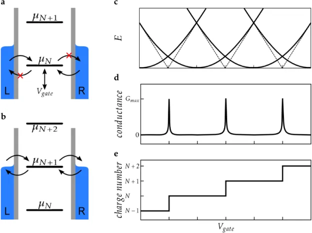
a
b
c
d
e
Figure 2.6: Coulomb blockade in a quantum dot at zero bias voltage. aChemical poten- tial of the dotµN lies below andµN+1above the lead potentials. Electrons can tunnel onto µN, but are unable to leave the dot, therefore the current is blocked. bPotential of the dotµN is aligned with the lead potentials. This allows charge fluctuations and the dot becomes conductive. cEnergy versus gate voltage: quadratic gate voltage dependence leads to parabolas. At the intersection point the energy forN andN+ 1 is equal which allows current flow.dThis results in peaks in the conductance at the corresponding gate voltage values.eFor each intersection point, the number of charges occupying the dot is increased by one.
If the chemical potential of the dot lies below the chemical potentials of the leads, charges can tunnel onto the unoccupied state but not out since they can not overcome the energy difference. The quantum dot is in Coulomb blockade (cf. Fig. 2.6a). If the chemical potentials of the leads and the dot align, the charge numbers on the dot can fluctuate and current can flow (cf. Fig. 2.6b).
Assuming the quantum dot to be a metallic island with a constant density of states, one can express the ground state energy of the dot by the classical charg- ing energy of a capacitor:
E(N)' 1 2CΣ
(eN+CgateVgate)2. (2.18) The condition for single electron tunneling can then be expressed as
µ=eαgateVgate+ e2 CΣ
N+1
2
=eαgateVgate+U
N+1 2
, (2.19)
where the ratio between the gate capacitance and the total capacitance was short- ened to the so called gate conversion factorαgate:
αgate≡ Cgate
CΣ . (2.20)
The quantum dot potential can be moved by the gate voltage. The voltage needed to align the next chemical potential of the dotµ(N+ 1) to the chemical potential of the leads is
∆Vgate= e αgateCΣ
= e
Cgate. (2.21)
Figure 2.6c-e depict the discussed properties of the QD. In panel c the electro- static energy in dependence of the gate voltage is shown. The parabolic behavior is a result of the quadratic dependence onVgate (Eq. 2.18). Each parabola refers to a state with different charge numberN and the dashed lines indicate the en- ergy difference between two states. At the intersection points of the parabolas, the charging energy forN andN+ 1 is equal and current can flow. This leads to peaks in the conductance, which are depicted in panel d. Panel e shows the aver- age charge number which increases stepwise by∆N = 1 every time a conductance peak is passed.
2.3.2 Quantum Coulomb Blockade
So far a metallic quantum dot with a constant density of states was assumed.
However in systems where the Fermi wavelength is on the scale of the device itself, the energy levels will be quantized. This quantization can be resolved in experiments if the thermal energy is smaller than the level spacing (∆kBT).
For instance the level spacing∆ of a particle in a box of size Ldepends on the
2.3. QUANTUM DOTS AND COULOMB BLOCKADE 15 dimensionality of the system:
∆= N 4
~2π2
mL2 (1D) (2.22)
∆= 1 π
~2π2
mL2 (2D) (2.23)
∆= 1
3π2N
13 ~2π2
mL2 (3D) (2.24)
Therefore a semiconductor quantum dot with a size of 100 nm has a level spacing of around 0.03 meV. Since the thermal energy at typical cryogenic temperatures (100 mK) is about 0.01 meV, the confinement energy∆ plays a role in the spec- trum of the quantum dot.
2.3.3 Coulomb Blockade at Finite Bias
Up to this point the quantum dot was only charged by providing energy via the gate electrode. By applying a bias voltage to the leads the difference of the chemical potentials of source and drainµs andµd can be varied respectively (eVbias=µs−µd). This interval betweenµsandµdis called the bias window and in the classical regime, transport through the dot can only take place if the chemical potential of the dot lies within it. Performing a bias spectroscopy measurement where bias and gate voltage are changed continuously while the current through the dot is measured one obtains a color plot of the current as a function ofVgate
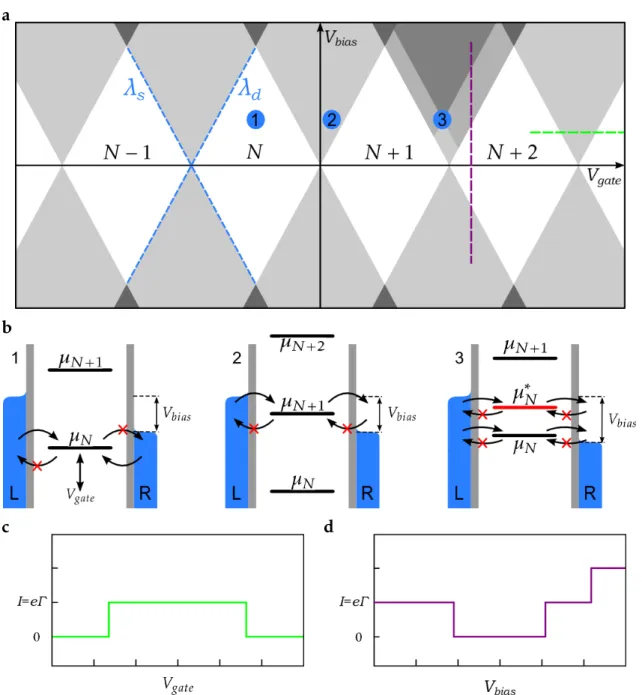
andVbias. This so calledcharging orstability diagramis depicted in Fig. 2.7a. In the white, diamond-shaped regions (blue circled 1 in Fig. 2.7a), no energy level is located inside the bias window and therefore no current through the dot is flowing. This pattern is known asCoulomb diamonds. The corresponding energy diagram (Fig. 2.7b sub-panel 1) shows that charges from both leads can tunnel into the dot, but cannot tunnel out, since the state of the dot lies below the chem- ical potentials of the leads. Therefore no current can flow. Increasing Vgate or Vbias correspondingly, one can get to areas (marked with 2), where one state lies within the bias window and therefore the blockade is lifted and current is al- lowed to flow. Increasing Vbias further, another chemical potential level enters the bias window, which leads to a stepwise increase of the current.
a
b
c d
Figure 2.7: Coulomb blockade at finite bias:aStability diagram of a quantum dot in the regime where the Coulomb diamond pattern appears. The blue dashed lines highlight the single electron lines for the source and drain contacts with their corresponding slopes λs andλd. bThe chemical potentials for different positions in the stability diagram. 1 Inside the white diamond shaped areas no current is flowing and the particle number, oc- cupying the dot, is constant.2A state of the quantum dot enters the bias window which allows current to flow. 3An additional excited state increases the number of transport channels and therefore the current. cCurrent versus gate voltage at finite bias voltage (cf. green line in panel a). When the line cut goes through the conducting region the cur- rent jumps from 0 toeΓ, leading to a rectangular shape.dCurrent versus bias voltage at a certain gate voltage (cf. purple line in panel a). Excited state in bias window increases current further.
2.3. QUANTUM DOTS AND COULOMB BLOCKADE 17 Taking the quantum regime of the transport into account, discrete levels as well as their excitations can be measured. There are two different types of changes in the tunneling current when Vbias is increased. The first one corresponds to the change of the number of charge states which are accessible in the bias win- dow. This situation is the same as in the classical case and the voltage difference between these current steps is calledaddition energy. The second type of current change is due to a change in the number of quantum states which can be occupied by an electron on the dot. This situation is illustrated in part 3 of Fig. 2.7b, where an excited stateµ∗N enters the bias windowµs > µN, µ∗N > µd. In this case the cur- rent is step-like increased since two charge transfer channels can contribute to the transport and therefore increase the tunneling probability. The voltage dif- ference for this type of current change is calledexcitation energy. The case of an excited level entering the bias window is presented in Fig. 2.7d, where the bias voltage dependence of the current is sketched at a gate voltage position, indicated by the purple dashed line in Fig. 2.7a.
The edges of the Coulomb diamonds, depicted as blue dashed lines in Fig. 2.7a, are calledsourceanddrainlines, along which the chemical potential of the source (drain) contactµs (µd) is aligned toµdot. According to Eq. 2.19, the dot potential along the drain line can be expressed as
µdot=µd =EN +
N+ 1 2
e2 CΣ
+e(αsVbias+αgateVgate) =const. (2.25) Also the source line can be written similarly
µdot=µs=EN +
N+1 2
e2
CΣ +e[(1−αs)Vbias+αgateVgate] =const. (2.26) One can now define additional conversion factors for source (αs) and drain (αd) contacts:
αs≡ Cs
CΣ, αd ≡ Cd
CΣ. (2.27)
With these two equations the slopes of the single electron lines (source line and drain line) can be determined as
λs ≡dVGate
dVbias =1−αs
αgate = CΣ−Cs
Cgate , (2.28)
λd ≡dVgate
dVbias =− αs
αgate =− Cs
Cgate. (2.29)
Therefore the gate conversion factorαgatecan be expressed as:
αgate= 1
|λs|+|λd|. (2.30)
2.3.4 Carbon Nanotube Quantum Dots
In carbon nanotube quantum dots three different transport regimes, depending on the transparency of the contact-tube interface, can be observed. In contrast to split gate defined heterostructure quantum dots, the transparency cannot eas- ily be controlled, but is set by the relation of the work function of the contact material and the nanotube. It can be varied by the gate voltage and is often dif- ferent for the hole and electron side of semiconducting nanotubes. This behavior is shown for instance in [41–43].
For high transparencies the CNT is in the so calledFabry-Pérot regime. It behaves like a one-dimensional coherent electron wave guide. The weak barriers at the contacts define a cavity whose transport behavior can be described as a Fabry- Pérot interferometer. In this regime, which was already mentioned in Ch. 2.2.1, the conductance can reach the limit of 4e2/h. For more opaque contact inter- faces and a conductance ofG .1.5e2/h, the system is in an intermediate trans- port regime where high order effects like cotunneling and the Kondo effect ap- pear [38, 44–46]. Therefore this regime is often referred to asKondo regime.
For low contact transparencies and a low conductance (G 1e2/h) Coulomb blockade dominates the transport and the system is in the so calledclosed regime.
Here single electrons tunnel sequentially through the dot, which is why such a device is often referred to as a single electron transistor (SET).
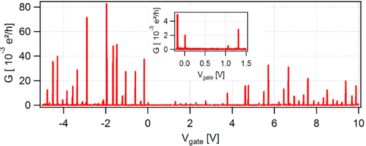
A stability diagram in the closed regime shows a pattern originating from the subsequent shell filling of the dot. This is presented in Fig. 2.8c. Due to the K/K’
and spin degeneracy, a fourfold pattern can be observed. This pattern is needed to extract important transport parameters of the device [48–50]. These parameters are the quantum energy level separation∆, the charging energyU, the subband mismatchδand the exchange energyJ. Figure 2.8a and b sketch the meaning of these energies. The exchange energyJ is equal to the energy difference between a parallel and anti-parallel spin configuration in two different orbital states. The band mismatchδis the small energy difference between the two branches and∆ is the energy spacing of two quantized levels of the CNT band structure.
2.3. QUANTUM DOTS AND COULOMB BLOCKADE 19 a
b
c
Figure 2.8: Shell filling of a CNT quantum dot. a Dispersion relation of a carbon nan- otube with discrete energy levels with a separation of∆. The subband mismatchδshifts the levels of the two branches slightly.bThe energy difference between two spins with a parallel and anti-parallel configuration in two different orbital states is called exchange energyJ. cStability diagram of a carbon nanotube quantum dot, which shows a four fold symmetry in the Coulomb diamond pattern. The sizes of the Coulomb diamonds vary between small, medium, small and large. The respective energies, which can be extracted, are labeled∆µifori∈ {1,2,3,4}. Adapted from [47].
According to [51] the Hamiltonian for the exchange interaction is defined as HJ=−J
2 X
σ=±
hnK,σnK0,σ+dK,σ† dK†0,−σdK,−σdK0,σ
i, (2.31)
wherenK,σ is the number of electrons with spin σ and pseudo-spinK and dK,σ(†) describes the removal (addition) of an electron with the quantum numbers K andσ. Assuming δ= 0, the following expressions for the addition energies can be written as:
∆µ1=U−J
2, (2.32)
∆µ2=U+3J
2, (2.33)
∆µ3=∆µ1, (2.34)
∆µ4=U+∆− J
2. (2.35)
Hereµi are the addition energies for specific charge numbersi∈ {1,2,3,4}within a fourfold degenerate shell.
2.4 Coherent Population Trapping
In Ch. 2.3 it was shown that the spatial confinement and the finite length of a CNT leads to discrete atom-like levels in its energy dispersion. Therefore these quasi 0D nanostructures are often referred to asartificial atoms[52]. This analogy suggests to transfer concepts of atomic physics to quantum dots [53].
2.4.1 Coherent Population Trapping in Optics
One effect of atomic physics is the coherent population trapping (CPT), where illumination of atoms can trap electrons into a coherent superposition of orbital states, which are completely decoupled from the dynamics and do not emit flu- orescent light [54–56]. Therefore these states are called dark states. They were observed for the first time by Alzetta et al. when sodium vapor was illuminated by a dye laser, in a way that the hyperfine splitting of the ground state matched the frequency difference of the two modes of the laser [57]. This observation was explained by Arimondo and Orriols in their analysis of a three level system in the folded (Λ-shaped) configuration [58]. This level system is depicted in Fig. 2.9.
Figure 2.9:Λ- shaped three level system of atomic levels. Two energy levels 1 and 2 have a common excited state 3. The corresponding optical transitions with frequenciesω21 andω31are depicted with dashed arrows.
They consider an atomic system consisting of two levels 1 and 2, which have a energy separation in the microwave region, and a common excited state 3. This level is coupled to the lower states by optical transitions at frequenciesω31and ω32. The laser which illuminates the system contains two coherent modes with frequenciesω1 andω2, amplitudesE1 andE2 and a phase differenceΦ. Its elec- tric field, polarized along the x-axis and propagating in the z-direction, can be described as
Ex(z, t) =1
2E1{exp[1(Ω1t−K1z0)] +c.c}+1
2E2{exp[1(Ω2t−K2z0+Φ)] +c.c}, where Ωi = ωi −Kivz and i = 1,2. The Doppler shift Kivz, due to the thermal motion of the atoms, along the z-direction is taken into account. Each laser mode
2.4. COHERENT POPULATION TRAPPING 21 is supposed to interact with only one optical transition. This approximation is valid for a mode separationω1−ω2 smaller than the optical linewidth. The in- teraction of the electromagnetic field with the atomic system is described by two generalized Rabi frequencies
α=µ13E1
2~ and β=µ23E2
2~ exp[iΦ], (2.36)
whereµ13andµ23are the electric dipole matrices.
In the rotating wave approximation, where rapidly oscillating terms are removed, the motion equations of the density matrixρcan be written as
˙
ρ11=iα( ˜ρ31−ρ˜13)−ρ11−ρ22
τ1
+f ρ33
T1
, (2.37)
˙
ρ22=iβ∗( ˜ρ32−ρ˜23)−ρ22−ρ11
τ1
+ (1−f)ρ33
T1
, (2.38)
˙
ρ33=iα( ˜ρ13−ρ˜31)−i(βρ˜23−β∗ρ˜32)−ρ33
T1
, (2.39)
˙˜
ρ13+i(∆−i/T2) ˜ρ13=iα(ρ33−ρ11)−iβ∗ρ˜12, (2.40)
˙˜
ρ23+i(∆0−i/T2) ˜ρ23=iβ∗(ρ33−ρ22)−iαρ˜21, (2.41)
˙˜
ρ12+i(∆−∆0−i/τ2) ˜ρ12=iαρ˜32−iβρ˜13, (2.42) where
∆=Ω1−ω31, ∆0=Ω2−ω32, ∆−∆0=Ω1−Ω2−ω21.
Here the relaxation processes are included withT1 as the relaxation time from the excited stateρ33,T2 the decay time for the optical coherencesρ13andρ31,τ2 as the time constant for the lower states coherenceρ12andτ1 as a relaxation time to produce equal populations in the lower states.f and 1−f are the probabilities for the decay in the states 1 and 2 respectively and the optical coherences are defined as
ρ13= ˜ρ13exp[i(Ω1t−K1z0)], (2.43) ρ23= ˜ρ23exp[i(Ω2t−K2z0)], (2.44) ρ12= ˜ρ12exp[i(Ω1−Ω2)t]. (2.45)
If one now substitutes ˜ρ13and ˜ρ23in Eq. 2.39 and assumes that both laser modes are in resonance with the optical transitions (∆=∆0 = 0), the expression forρ33 results in
ρ33= 2α2T1T2(ρ11−ρ33) + 2β2T1T2(ρ22−ρ33) + 4αβT1T2Re( ˜ρ12). (2.46) Assuming that the optical transitions 1-3 and 2-3 act separately one can show that ˜ρ12is a negative real quantity. Therefore the interference, which is the third term in Eq. 2.46, leads to a decrease in the excited state populationρ33.
Following the analysis of Brewer and Hahn [59] one obtains a solution for
Eq. 2.37 - 2.42 andρ33can be plotted where one laser mode is kept in resonance (∆= 0) while the frequency of the other is swept through the resonance condition for the two quantum Raman transition connecting the two ground states 1 and 2:
∆0−∆=ω21−(ω1−ω2)−(K2−K1)vz= 0. (2.47) Figure 2.10 shows thatρ33has a minimum value in a narrow region near the res- onance with linewidth fixed by the relaxation time of the ground state coherence τ2. Therefore the excited state is completely depopulated, when both laser exci- tations are in resonance.
Figure 2.10: Excited state occupation as a function of the resonance parameter (∆0−∆)T2. Applied parameters:∆= 0,αT2=|β|T2= 0.1,Φ= 0,τ2=τ1= 105T2and T1=T2/2. The minimum value ofρ33is 9·10−6.Taken from [58]
In summary this means, that Raman transitions connecting the levels 1 and 2 create a coherence of the lower states which decreases the net number of transi- tions from the lower states to the excited state, through the interference term in
2.4. COHERENT POPULATION TRAPPING 23 Eq. 2.46. This interference phenomenon occurs each time the mode separation matches the ground state splitting.
2.4.2 All Electronic Coherent Population Trapping
An analogue without laser illumination of coherent population trapping in quan- tum dots was presented by Michaelis et al. [60]. In a system containing three tunnel-coupled quantum dots, an electron can become trapped in a coherent su- perposition of states in different dots, which blocks the current flow through the system due to Coulomb blockade. For the sake of clarity only the main results are presented. Further details can be found in [60].
In this concept the bias voltage plays the role of the laser illumination, as de- scribed in Ch. 2.4.1.
Figure 2.11: System of three quantum dots, in which a dark state can form. The tran- sitions from the source contacts to the quantum dots A and B, and from C to the drain electrode are unidirectional with a tunneling rateΓ. The interdot transitions are labeled withT and are reversible. Sketch adapted from [60].
Figure 2.11 shows the scheme of the three-dot system. The transitions from the leads on the left side to the dots Aand B as well as from the dotC to the lead to the right are irreversible due to the bias voltage. They are described by the following jump operators with a tunneling rateΓ:
LA=
√
Γ|Ai h0|, LB=
√
Γ|Bi h0|, LC =
√
Γ|0i hC|, (2.48) where|0iis the state in which all three dots are empty. The energies of the single particle levels|Ai,|Bi,|Ciare set to zero, to neglect inelastic transitions between
these levels. The elastic transitions between the three quantum dots, with a tun- neling rateT are reversible and are described by a tunneling Hamiltonian:
H=T|Ci hA|+T|Ci hB|+H.c.=
√
2T|Ci hΦ+|+h.c. (2.49) The superposition of states|Aiand|Biis defined as
|Φ±i= 1
√
2(|Ai ± |Bi). (2.50) The dynamics of such a device can be studied by a master equation approach which gives the time evolution of the three-dot density matrixρ(t):
dρ
dt =−i[H, ρ] + X
X=A,B,C
LXρL†X−1
2L†XLXρ−1
2ρL†XLX
. (2.51)
For the basis of the density matrix the four states of the system are used:
|e1i=|Φ+i, |e2i=|Φ−i, |e3i=|Ci, |e4i=|0i, (2.52) The stationary result of Eq. 2.51 is
tlim→∞ρ(t) =|Φ−ihΦ−|, (2.53) meaning that, without any sort of decoherence, the electron is trapped in the an- tibonding superposition of the two states|Aiand|Bi.
This result shows that the effect of coherent population trapping can be achieved without laser illumination, allowing to transfer the CPT concept to an all elec- tronic analogue.
2.4.3 Coherent Population Trapping in Carbon Nanotubes
If one wants to transfer this scheme of charge population trapping to a single quantum dot, an orbital degree of freedom and a source of coherence in the cou- pling to the leads is needed. In a carbon nanotube quantum dot the first require- ment is easily met, since for low energies the valley degree of freedom can be mapped on the orbital one.
In the following segment it will be shown, that electrons which tunnel from the lead to the CNT generally acquire an orbital phase providing coherence. The pre- sentation follows the reference [61]:
In general the tunneling Hamiltonian is written as Htun= X
α~kmlzσ
tα~kml
zdml†
zσcα~kσ +h.c., (2.54)
2.4. COHERENT POPULATION TRAPPING 25 wheredml†
zσ creates an electron in the CNT in shell m with angular momentum lz=±l and spinσ =↑,↓. cα~kσ destroys one electron in the leadα=L, Rwith spin σ and momentum~k. The tunneling amplitude tα~kml
z is the overlap of the wave function of the leadΨα~kσ(~r) =h~r|α~kσiand of the CNTΦmlzσ(~r) =h~r|mlzσi. It can be written as
tα~kml
z= Z
lead
d~rΨ∗
α~kσ(~r) p2
2mel +v(~r)
!
Φmlz(~r). (2.55) The wave function of the CNT is much more localized than the one of the lead.
Therefore the contribution of the lead Hamiltonian to the overlap can be ne- glected. The electronic properties of the atomic orbitals|j
are mainly given by pz orbitals, which are assumed to be delta-likeh~r|ji=δ(~r−R~j) at the atomic posi- tionR~j. This leads to the following expression for the tunneling amplitude:
tα~kml
z=mhα~kσ|mlzσi=mX
j
Z
d~rhα~kσ|~rih~r|jihj|mlzσi=mX
j
hα~kσ|~Rjihj|mlzσi. (2.56)
Figure 2.12: Sketch of a ring of carbon atoms standing on a metallic contact, in a way that only one atom touches the surface.
For zigzag-CNTs or carbon nanotubes with small chiral angles the wave function along the tube does not change in the small region of the contact. Therefore the tube can be simplified to a ring with radiusRofN carbon atoms. The shell index mcan be dropped which leads to|mlzσi → |lzσiandm=. The ring Hamiltonian can then be expressed as:
hj|lzσi= 1
√
Nei2πNjlz. (2.57)
The carbon ring is now placed standing on the lead in the y-z plane, as shown in Fig. 2.12. The wave function of the lead can be split into plane waves parallel to the surface and a perpendicular part which is exponentially decaying
Ψα~kσ(~r) =Ψαkk
ykzσ(y, z)Ψαk⊥
xσ(x)∝ei(kyy+kzz)e−καxx, (2.58)
![Figure 3.2: a Basic principle of a dilution refrigerator. Sketch adapted from [124]. b Photograph of the actual dilution refrigerator used in this work](https://thumb-eu.123doks.com/thumbv2/1library_info/3853168.1516204/52.892.131.729.165.546/figure-principle-dilution-refrigerator-sketch-photograph-dilution-refrigerator.webp)
![Figure 3.6: Voltage noise S V versus current: Close to the pinch o ff point at V gate = 0.468 V (black curve), the Fano factor is assumed to be F = 1.0 [89]](https://thumb-eu.123doks.com/thumbv2/1library_info/3853168.1516204/57.892.183.673.191.493/figure-voltage-noise-versus-current-close-factor-assumed.webp)