Journal of Physics D: Applied Physics
PAPER • OPEN ACCESS
Electrical detection of ferromagnetic resonances with an organic light- emitting diode
To cite this article: Tobias Grünbaum et al 2019 J. Phys. D: Appl. Phys. 52 485108
View the article online for updates and enhancements.
This content was downloaded from IP address 132.199.145.195 on 28/11/2019 at 12:42
Introduction
Organic light-emitting diodes (OLEDs) constitute an appealing model system for investigating spin-dependent transport and recombination phenomena in condensed matter physics. A tool for direct access to the spin symmetry of charge-carrier pairs in OLEDs is electron paramagnetic resonance (EPR) spectr- oscopy, where resonant transitions between singlet and triplet- like carrier pairs are driven by high-frequency excitation. In
contrast to conventional polarization-based EPR, the impact of resonant changes on spin permutation symmetry is so sub- stantial that resonances are readily observed under DC detec- tion conditions of the device current. Strong driving of the charge-carrier spins reveals coherent phenomena such as the spin-Dicke effect [1], where an inversion of the resonance fea- ture is observed due to collective behavior of the individual resonant spins. As it is challenging to generate the high radio- frequency (RF) excitation fields necessary to observe these effects, new experimental solutions of this issue are desirable [2, 3]. It is conceivable that magnetic fringe fields originating from ferromagnetic resonance (FMR) in a proximate magn- etic sample could be suitable to act as the driving field for EPR experiments. However, besides this dynamic magnetic field effect, also a thermal influence of a magnetic film on an
Journal of Physics D: Applied Physics
Electrical detection of ferromagnetic
resonances with an organic light-emitting diode
Tobias Gr ü nbaum
1,3, Sebastian Bange
1, Matthias Kronseder
1, Christian H Back
2and John M Lupton
11 Institut für Experimentelle und Angewandte Physik, Universität Regensburg, Universitätsstraße 31, 93053 Regensburg, Germany
2 Physics Department, Technische Universität München, James-Franck-Str. 1, 85748 Garching, Germany E-mail: tobias.gruenbaum@ur.de
Received 27 May 2019, revised 17 July 2019 Accepted for publication 15 August 2019 Published 16 September 2019
Abstract
Organic semiconductors show strong magnetic-field effects in transport and luminescence because of inherently spin-dependent recombination. We explore whether paramagnetic resonance features can be enhanced in a hybrid structure comprising a thin yttrium iron garnet (YIG) film, undergoing ferromagnetic resonance (FMR) and an organic light-emitting diode (OLED). We investigate the effect of radio-frequency (RF) driving of this hybrid structure in a magnetic field. Under these conditions, an indirect bolometric effect enables the detection of FMR driven in the YIG film in the DC resistance of the OLED. The increased RF power absorption of the YIG film under resonance gives rise to a heating of the magnetic film.
Subsequent heat transfer to the OLED causes a change in transport characteristics of the device. Good agreement of this electrically detected signal is found with a direct measurement of the RF power absorption. Using temperature dependent measurements, the thermal nature of the resistance signal is confirmed.
Keywords: ferromagnetic resonance, yttrium iron garnet, organic light-emitting diodes S Supplementary material for this article is available online
(Some figures may appear in colour only in the online journal)
T Grünbaum et al
Printed in the UK 485108
JPAPBE
© 2019 IOP Publishing Ltd 52
J. Phys. D: Appl. Phys.
JPD
10.1088/1361-6463/ab3b6c
Paper
48
Journal of Physics D: Applied Physics IOP
Original content from this work may be used under the terms of the Creative Commons Attribution 3.0 licence. Any further distribution of this work must maintain attribution to the author(s) and the title of the work, journal citation and DOI.
3 Author to whom any correspondence should be addressed.
2019
1361-6463
https://doi.org/10.1088/1361-6463/ab3b6c J. Phys. D: Appl. Phys. 52 (2019) 485108 (6pp)
T Grünbaum et al
2
OLED is expected to arise due to the increased power absorp- tion of the ferromagnet under FMR conditions. In order to characterize this thermal effect, we study a hybrid device con- sisting of an OLED and an yttrium iron garnet (YIG) film.
In their simplest form, OLEDs consist of an organic semi- conductor sandwiched between two electrodes, as shown in figure 1(a). Application of a voltage between anode and cathode leads to charge-carrier formation at the interfaces between the electrode and the organic semiconductor and therefore to injection into the semiconductor. The excess charges on these molecules then drift through the device via hopping between different molecular sites. As the hopping transport is thermally assisted, an increase of the device con- ductivity is commonly found upon increasing the temperature [4, 5]. Recombination of positive and negative charge carriers eventually gives rise to light emission. According to the pair mechanism of magnetoresistance, the density of free charge carriers and therefore the OLED resistance can be manipu- lated by the application of an external magnetic field [6]. We investigate the influence of a magnetic film under strong high- frequency driving on the device resistance of an OLED. If such a film is subject to a high-frequency magnetic field H
1, precession of the magnetization M is driven around its equi- librium position along the direction of the effective magn etic field
Heff =H0+H1+Hdemag+Hani, where
Hdemagis the demagnetizing field and
Haniis the anisotropy field. By tuning the external magnetic field strength H
0, the condition of FMR can be reached, where the precession cone angle and the RF power absorption reach maximum values [7, 8]. A common method to detect FMR is to measure the reduction of the trans- mitted RF power on resonance [8, 9].
Experimental results and discussion
Detection of FMR with an OLED
We perform FMR measurements with a sample consisting of a magnetic film in close proximity to an OLED. We use a 5 µm-thick YIG film as the ferromagnetic sample, grown on a gadolinium gallium garnet (GGG) substrate by liquid- phase epitaxy. The OLED consists of several layers of metals and organic semiconductors. From a glass substrate covered with a 100 nm-thick layer of indium tin oxide (ITO) a rect- angular electrode is defined by an etching process. An 80 nm-thick layer of poly(styrene-sulphonate)-doped poly(3,4- ethylene-dioxythiophene) (PEDOT:PSS), which serves as the hole-injection layer, is spin-coated on top of the ITO anode after various standard cleaning steps which ensure a smooth surface of the PEDOT:PSS layer. A 90 nm-thick film of the commercial poly(phenylene-vinylene) (PPV) copolymer
‘ SuperyellowPPV ’ (SyPPV, Merck AG) is spin-coated on top as the light-emitting material, which in turn is contacted by a thermally evaporated cathode consisting of 3 nm of barium and 250 nm of aluminum. Barium serves as an electron injec- tion layer due to its low work function. To ensure a good contact between the YIG film and the OLED, the YIG film is affixed on top of the cathode with a two-component epoxy glue inside a nitrogen glovebox, which also serves to protect
the device against oxidation. Details of the device character- ization are given in figure S1
4.
The experiment is based on a conventional waveguide- FMR setup. RF radiation coming from an Anritsu MG3740A analog signal generator is amplified to up to 20 W by an HD Communications HD31253 broadband RF amplifier.
The sample structure is placed on the signal line of a copper coplanar waveguide, which is designed to match a 50 Ω impedance with a conductor thickness of 35 µm, a width of 4 mm and a 0.5 mm spacing between center and ground con- ductors. At an RF power of P = 1 W, the excitation field at the position of the YIG film is calculated to be approximately µ
0H
1= 20 µT. Using a Keysight 33330C coaxial Schottky- diode detector, the transmitted RF power is converted to a DC voltage, which is then measured with a Keysight 34461A multimeter. To protect the Schottky diode from damages due to overly high incident power, a directional coupler was used to reduce the transmitted RF power by 25 dB. A Keithley 238 high-current source measure unit simultaneously served as the power supply for the OLED, operated under constant voltage conditions and also recorded the device resistance. A set of Helmholtz coils driven by a CAEN ELS Easy Driver 0520 bipolar power supply produced an external magnetic field of µ
0H
0, tunable from −30 mT to 30 mT, applied in the sample plane. FMR spectra were recorded under continuous RF exci- tation at a fixed frequency by sweeping H
0. No modulation technique was employed so that only changes in DC conduc- tivity were recorded.
RF absorption measurements were performed with an RF excitation power of P = 3.25 W. The resulting FMR spectra shown in figures 1(b) – (d) feature distinct absorption peaks, whose shape and number depend on the excitation frequency f . For f = 0.9 GHz, broad peaks around µ
0H
0= ±3 mT are observed in figure 1(b). At higher excitation frequencies of 1.4 GHz and 1.9 GHz, shown in (c) and (d), these absorption peaks corresponding to the uniform precession of the mag- netization (i.e. at momentum q = 0, the so-called uniform mode) can be distinguished from an additional broad feature at lower magnetic fields. This feature is usually referred to as the subsidiary absorption or first-order Suhl instability and originates from a spin-wave instability. Under strong RF excitation, transverse driving of spin waves with finite wave vector q ≠ 0 resonant at half the excitation frequency occurs [10, 11]. This phenomenon is also well established in YIG samples for different excitation arrangements [12, 13]. Frequency-dependent measurements of the positions of the two peaks, shown in figure 2(a), indicate that the peak positions for the uniform mode and for subsidiary absorp- tion conv erge for low frequencies until they cannot be distin- guished anymore at frequencies below 1 GHz. With an OLED placed in close proximity to the YIG film, the absorption peaks in the transmitted power measured by the Schottky diode are accurately reproduced in the OLED resistance. Following the nomenclature from previous studies [14 – 16], we refer to the
4 See the online supplementary material at (stacks.iop.org/JPhysD/52/485108/
mmedia) for details about the characterization of the SyPPV OLED and the YIG sample.
J. Phys. D: Appl. Phys. 52 (2019) 485108
FMR signal in the OLED resistance as ‘ electrically detected ferromagnetic resonance ’ (EDFMR). Forward and backward sweeps of the external magnetic field in figure 1(c) reveal a shift of the EDFMR peaks with respect to the Schottky- diode absorption peaks, which is indicative of a temporal lag between the two measurement results. We conclude that this lag suggests a time constant on the timescale of seconds for the effect which causes the EDFMR signal in the OLED resistance.
To verify the physical origin of the FMR signature in the OLED resistance, frequency and power-dependent measurements were performed. FMR measurements at a power of P = 3.25 W were carried out with the excitation frequency ranging from f = 0.6 GHz to f = 2.1 GHz. The observed peak positions in RF absorption yield the expected depend ence of the resonance field of the FMR uniform mode, H
FMR, on the excitation frequency, which is given by
µ0HFMR=−µ02Meff +…ĵ0Meff
2
ä2
+Ä2πf
γ
ä2
for a thin magn- etic film without in-plane magneto-crystalline anisotropies under an in-plane external magnetic field of H
0. As plotted in figure 2(a), the data are well described by µ
0M
eff= 171 mT and γ = 1.77 × 10
11rad Ts
−1, in good agreement with litera- ture values [17, 18]. These values were obtained in an inde- pendent characterization of the YIG film by both in-plane and out-of-plane low-power FMR measurements on a different
setup and by measurements of the polar magneto-optical Kerr effect as discussed in figure S2 of the supplementary mate- rial. Peak positions of the EDFMR signal are determined by
Figure 1. FMR detected by an OLED. (a) Schematic of the sample structure: an OLED and a YIG film of 5 µm thickness grown on a GGG substrate are brought into close contact by encapsulation with two-component epoxy. High-frequency excitation from a coplanar waveguide induces precession of the magnetization around the equilibrium position in the YIG film. In (b)–(d) the power absorption measured by a Schottky diode (blue) and the relative resistance change of the OLED (red) are shown as a function of the externally applied magnetic field µ0H0 for three values of the excitation frequency. At higher frequencies, the narrow FMR peak can be clearly distinguished from the broader subsidiary absorption band. This latter feature arises at lower fields due to parametric amplification of spin waves and is readily distinguished from the narrow FMR peak by its frequency dependence. Dotted lines in (c) indicate a reversal of field sweeping direction.
Good agreement between the absorption and the resistance signal is observed. All experiments were carried out in DC mode, i.e. without modulation.
Figure 2. (a) Frequency dependence of the resonance field values detected by RF absorption measured with the Schottky diode (blue crosses) and through the OLED resistance (red open circles).
Peak positions are shown for both the uniform mode and for subsidiary absorption. The line shows the behavior expected from the resonance condition as stated in the main text, with parameters obtained from a low-power FMR characterization of the sample.
(b) Power dependence of the relative change in OLED resistance at the uniform-mode FMR peak at 0.9 GHz, on a double-logarithmic scale. The data lie on a straight line of slope unity.
T Grünbaum et al
4
taking the mean value of forward and backward sweeps of the external magnetic field. For frequencies below 1 GHz, the subsidiary absorption dominates both the FMR and the EDFMR signal, so that the uniform mode is not resolved as a distinct peak anymore. As summarized in the plot of the frequency dependence of the resonance field in figure 2(a), excellent agreement with the peak positions found in the absorption measurements is established, proving that both the uniform mode and the subsidiary absorption peaks are identified in EDFMR. While the frequency range accessible in this study is limited by the RF equipment, these observa- tions are expected to extend to any excitation frequency for which stable FMR can be induced in the YIG film. We found that the EDFMR signal is still detectable at excitation powers as low as 50 mW.
Identification of an indirect bolometric effect
As heating of the YIG film under FMR is expected to become more significant with greater RF excitation powers, a thermal origin of the EDFMR signal suggests itself. In this scenario, the linear relationship which exists between RF excitation power and FMR intensity should be transferred to the EDFMR signal [15, 19]. To verify this hypothesis, FMR measurements were performed at f = 0.9 GHz and the RF input power was varied from 0.02 W to 20 W. To account for waveguide losses, the power incident on the magnetic sample is calculated as the mean of ingoing and outgoing power of the coplanar waveguide. From the mea- sured spectra, the EDFMR amplitude is extracted as the dif- ference between baseline and peak resistance, corrected for the temperature-dependent off-resonant resistance change as outlined in the supplemental material and plotted as a func- tion of the averaged RF power in figure 2(b). On a double- logarithmic scale, the resulting data is well approximated by a straight line through the origin with slope one, verifying the expected linearity. This result is in agreement with sev- eral earlier studies [14, 15, 19], where the electrical detec- tion of FMR in the resistance of magnetic films due to a bolometric effect was investigated.
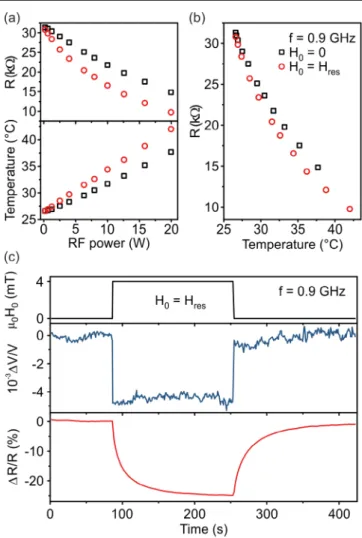
A direct proof of the thermal origin of the OLED EDFMR signal is obtained by investigating the temperature depend- ence of the OLED resistance under both off-resonant and res- onant conditions. Under continuous RF excitation at f = 0.9 GHz, the temperature of the sample is varied by changing the excitation power and thereby the losses arising in the CPW.
Measuring the temperature on the back side of the OLED with a thermocouple yields a linear relationship with the input RF power, shown as black squares in the lower panel of figure 3(a). In the resonant case, indicated by red circles, the temperature at a given power is substantially higher than off resonance. Simultaneously, in the upper panel of figure 3(a), for both off-resonant and resonant conditions, a decrease of the device resistance is observed with increasing temper- ature. This change in resistance demonstrates thermal con- tact between the individual components of the sample and shows that additional heating of the OLED takes place under resonance. Combining these two observations leads to the
conclusion that when the magnetic field is raised from zero to the resonance field (i.e. µ
0H
0= 3 mT), the temperature of the OLED is further increased by resonant heating of the YIG film and the subsequent thermal conduction, which in turn affects the device resistance. Plotting the OLED resistance against the temperature measured with the thermocouple in figure 3(b) illustrates that higher temperatures and hence lower resist- ances are reached in the device structure under resonance than off resonance. These resistance-temperature characteristics of both the off-resonant and the resonant behavior are similar as would be expected for a purely bolometric effect of the reso- nance on device operation. The difference in the characteris- tics is explained by the fact that the temperature is measured at the back of the OLED glass substrate, which is in contact with air at room temperature. The temperature increase of the emissive layer on resonance, which is actually responsible for the change in resistance signal, is therefore not expected to be fully reproduced by the measurement with the thermocouple.
From these observations we can infer conclusively that a bolo- metric effect — rather than, for example, an increase in local
Figure 3. (a) OLED resistance and temperature as a function of the applied RF power. (b) The device temperature, measured with a thermocouple and plotted against the device resistance, shows a correlation with the device resistance for resonant (red) and off-resonant (black) conditions, indicating a thermal origin of the EDFMR signal. (c) Temporal evolution of the RF absorption (blue line) and the resistance signal (red line). The magnetic field (black line) is abruptly changed from zero to the resonance field and back again.
J. Phys. D: Appl. Phys. 52 (2019) 485108
oscillating magnetic field amplitude — is the dominant mech- anism behind the EDFMR signal.
The slow temporal evolution of the EDFMR effect noted above can be examined by switching between resonant and off-resonant conditions. Under continuous RF excitation at f = 0.9 GHz and P = 10 W, the voltage of the Schottky diode remains constant, as does the OLED resistance. As shown in figure 3(c), sudden switching of the external magnetic field strength to the resonance field is accompanied by a step-like decrease of the Schottky-diode signal, a consequence of the increased power absorption of the YIG film under FMR.
However, the OLED resistance increases on a much longer timescale, on the order of tens of seconds. The same behavior is observed when FMR is turned off again by lowering the magnetic field back to zero. This result of slow heating and cooling under resonance is in good agreement with prior observations made by Gui et al in studying the electrical transport characteristics of magnetic films [15]. Moreover, the shift between FMR and EDFMR spectra as shown in figures 1(b) – (d) is readily explained by the long timescale of the OLED temperature change. Upon reaching the resonance condition, it takes several seconds for the OLED to reach its maximum temperature, leading to a shift of the EDFMR curve on the magnetic-field axis, i.e. a lag between EDFMR and FMR curves in the sweep direction. If the magnetic field is increased beyond the resonance field, the temperature of the OLED relaxes again on the timescale of several seconds, causing a slight broadening of the EDFMR peaks with respect to the FMR peaks. In combination with the linear power dependence of the EDFMR signal amplitude and the temper- ature dependence of the OLED resistance, this transient evo- lution of the EDFMR signal corroborates the picture that EDFMR originates from heating of the YIG film under FMR and subsequent heat transfer to the OLED with the associated change in resistance.
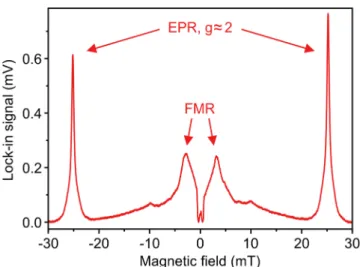
Finally, we also note that it is possible to detect simultane- ously the spin- ½ EPR of the carrier spins in the OLED current, i.e. electrically detected magnetic resonance (EDMR) and EDFMR. Since the EDMR signal is much weaker, we have to resort to modulated lock-in detection as described previ- ously [20]. Also, because the EDMR signal, which arises from spin-dependent recombination and the mixing of singlet and triplet exciton-precursor electron – hole pairs under resonance, appears at higher magnetic fields than the EDFMR signal, we are limited in frequency due to the finite sweep range of the electromagnet employed. Figure 4 shows the resistance change of the ferromagnet–OLED hybrid structure under res- onant drive at f = 700 MHz and a power level of P = 3.25 W, which clearly reveals the EPR and the FMR features. The EPR feature arises around a g factor of approximately two as expected [20].
Outlook and conclusions
Although the bolometric effect described above pre- vails at strong driving power, it is also conceivable that a
magnetoresistive effect could arise from magnetic fringe fields [21, 22] with components oscillating at the magnetiza- tion precession frequency. Under the given experimental con- ditions, however, we expect this effect to be negligible. The magnitude of the oscillating field strength can be estimated by calculating the static stray field of the YIG sample from the dimensions and magnetization of the film [23]. For a spatially homogeneous value of the magnetization of 140 kA m
−1and dimensions of 6 mm × 7 mm × 5 µm, static stray fields on the order of 100 µT are expected along the z-axis of the sample.
As the magnetization precession angle during FMR does not exceed a few degrees [24], the oscillating comp onents of the stray fields will at most be of the order of a few µT. We there- fore expect that the effect of oscillating fringe fields will be negligible given the overall magnetoresistance characteris- tics of a SyPPV OLED shown in figure S1(b). We note that the magnitude of oscillating fringe fields may be increased by optimizing the design of the magnetic sample and its arrangement with respect to the OLED. By maximizing the static and most importantly the dynamic stray fields with an appropriate geometry — and minimizing thermal contact to prevent the bolometric effects discussed here — it should be possible to generate high oscillating magnetic field strengths.
This approach might provide interesting new possibilities for performing high-frequency magnetic resonance excitation experiments in OLEDs, especially with regards to the regime of ultrastrong driving where the Rabi frequency approaches the carrier-wave frequency [1 – 3].
We conclude that thermal effects as observed here have to be considered when interpreting resistance or voltage sig- nals arising in hybrid structures of organic semiconductors and magnetic thin films. Although several prior reports of the inverse spin-Hall effect driven by FMR have discussed the conditions under which heating effects should be negli- gible [18, 25], our results may be of relevance particularly in the regime of high c.w. excitation powers. In addition to
Figure 4. Simultaneous detection of EPR and FMR in electrically detected magnetic resonance (EDMR) of a ferromagnet-OLED hybrid structure at f = 700 MHz. To be able to clearly resolve both features, lock-in detection with square modulation of the RF amplitude at 23 Hz was employed.
T Grünbaum et al
6
voltage generation by the Seebeck effect as outlined in [26], also heating due to resonant microwave absorption in the fer- romagnet may occur, suggesting some caution may be apt in interpreting spin-pumping experiments employing organic semiconductors. The inherently low heat capacity of OLEDs is often considered detrimental to device operation [27]. Here, we exploit this feature to resolve FMR features with an OLED.
Ultimately, we expect to be able to integrate ferromagn etic nanoparticles directly within an OLED. Given the facile scal- ability of OLEDs down to submicron dimensions [28], it would also be conceivable to design a pixelated structure or to employ luminescence mapping as demonstrated in [5] in order to image the FMR directly in real space.
Acknowledgments
The authors are indebted to the DFG for financial support through the SFB 1277 projects B03 and A08 as well as to Dr Lin Chen and Dr Hans Malissa for insightful discussions.
ORCID iDs
Tobias Gr ü nbaum https://orcid.org/0000-0003-4065-5442 References
[1] Waters D P, Joshi G, Kavand M, Limes M E, Malissa H, Burn P L, Lupton J M and Boehme C 2015 Nat. Phys.
11 910
[2] Jamali S, Joshi G, Malissa H, Lupton J M and Boehme C 2017 Nano Lett. 17 4648
[3] Bayliss S L, Greenham N C, Friend R H, Bouchiat H and Chepelianskii A D 2015 Nat. Commun. 6 8534 [4] Gärditz C, Winnacker A, Schindler F and Paetzold R 2007
Appl. Phys. Lett. 90 103506
[5] Buytaert J, Bleumers J, Steen A and Hanselaer P 2013 Org.
Electron. 14 2770
[6] Wagemans W and Koopmans B 2011 Phys. Status Solidi b 248 1029
[7] Kittel C 1948 Phys. Rev. 73 155
[8] Heinrich B 1994 Ultrathin Magnetic Structures II ed B Heinrich and J A C Bland (Berlin: Springer) (https://doi.
org/10.1007/b138706)
[9] Celinski Z, Urquhart K B and Heinrich B 1997 J. Magn.
Magn. Mater. 166 6
[10] Suhl H 1956 Phys. Rev. 101 1437
[11] An S Y, Krivosik P, Kraemer M A, Olson H M, Nazarov A V and Patton C E 2004 J. Appl. Phys. 96 1572
[12] Jantz W and Schneider J 1975 Phys. Status Solidi a 31 505 [13] Sandweg C W, Kajiwara Y, Chumak A V, Serga A A,
Vasyuchka V I, Jungfleisch M B, Saitoh E and Hillebrands B 2011 Phys. Rev. Lett. 106 216601 [14] Goennenwein S T B et al 2007 Appl. Phys. Lett. 90 162507 [15] Gui Y S, Mecking N, Wirthmann A, Bai L H and Hu C-M
2007 Appl. Phys. Lett. 91 082503
[16] Tu S, Bialek M, Zhang Y, Zhao W, Yu H and Ansermet J-P 2017 J. Magn. Magn. Mater. 439 53
[17] Haertinger M, Back C H, Lotze J, Weiler M, Geprägs S, Huebl H, Goennenwein S T B and Woltersdorf G 2015 Phys. Rev. B 92 054437
[18] Ando K, Watanabe S, Mooser S, Saitoh E and Sirringhaus H 2013 Nat. Mater. 12 622
[19] Gui Y S, Holland S, Mecking N and Hu C-M 2005 Phys. Rev.
Lett. 95 056807
[20] Baker W J, Ambal K, Waters D P, Baarda R, Morishita H, van Schooten K, McCamey D R, Lupton J M and Boehme C 2012 Nat. Commun. 3 898
[21] Salis G, Alvarado S F, Tschudy M, Brunschwiler T and Allenspach R 2004 Phys. Rev. B 70 085203
[22] Wang F, Macià F, Wohlgenannt M, Kent A D and Flatté M E 2012 Phys. Rev. X 2 021013
[23] Engel-Herbert R and Hesjedal T 2005 J. Appl. Phys.
97 074504
[24] Costache M V, Watts S M, Sladkov M, van der Wal C H and van Wees B J 2006 Appl. Phys. Lett. 89 232115
[25] Sun D, van Schooten K J, Kavand M, Malissa H, Zhang C, Groesbeck M, Boehme C and Vardeny Z V 2016 Nat.
Mater. 15 863
[26] Wang P, Zhou L F, Jiang S W, Luan Z Z, Shu D J, Ding H F and Wu D 2018 Phys. Rev. Lett. 120 047201
[27] Lupton J M 2002 Appl. Phys. Lett. 80 186
[28] Boroumand F A, Fry P W and Lidzey D G 2005 Nano Lett. 5 67
J. Phys. D: Appl. Phys. 52 (2019) 485108