Exercise 2: PS/2 keyboard
G. Kemnitz ∗ , TU Clausthal, Institute of Computer Science May 22, 2012
Abstract
First a simple given receiver for PS/2 data packages has to be checked with the logic analyzer. Afterward the function should be improved.
1 PS/2 protocol
The FPGA board has a 6-pole mini-DIN connector to plug in a PS/2 keyboard or a PS/2 mouse (figure 1).
1 5
3 2 4
6
Pin Function 1
2 3 4 5 6
Data Reserved GND Vdd Clock Reserved Figure 1: Connector to plug in PS/2 devices
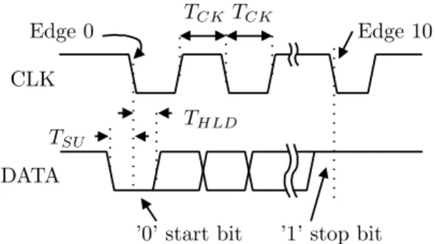
PS/2 defines a synchronous serial protocol (see figure 2). Each PS/2 data package consists of 11 bits
• 1 start bit (zero)
• 8 data bits
• 1 parity bit (odd parity)
• 1 stop bit (one)
which are after another submitted via the the same wire. An additional clock signal informs the receiver, when the data bits are valid.
if there is no transmission the data and the clock line are one (start bit). The transmission starts with a falling edge of the data line to zero. A time T SU later the clock first changes to zero an has in total 11 falling and 11 rising edges.
The times between clock edges must be in the interval:
∗