Magnetic field control of the Franck-Condon coupling of few-electron quantum states
P. L. Stiller, 1 A. Dirnaichner, 1 D. R. Schmid, 1 and A. K. Hüttel 1,2,*
1
Institute for Experimental and Applied Physics, University of Regensburg, 93040 Regensburg, Germany
2
Low Temperature Laboratory, Department of Applied Physics, Aalto University, P.O. Box 15100, FI-00076 Aalto, Finland
(Received 6 December 2018; revised 18 August 2020; accepted 20 August 2020; published 9 September 2020) Suspended carbon nanotubes display at cryogenic temperatures a distinct interaction between the quantized longitudinal vibration of the macromolecule and its embedded quantum dot, visible via Franck-Condon con- ductance sidebands in transport spectroscopy. We present data on such sidebands at known absolute number N
el= 1 and N
el= 2 of conduction band electrons and, consequently, well-defined electronic ground and excited states in a clean nanotube device. The interaction evolves only at a finite axial magnetic field and displays a distinct magnetic-field dependence of the Franck-Condon coupling parameter, different for different electronic base states and indicating a valley dependence. Reshaping of the electronic wave function by the magnetic field is discussed as a possible cause of our observations; its impact is demonstrated in a model calculation reproducing the field-dependent coupling.
DOI: 10.1103/PhysRevB.102.115408
I. INTRODUCTION
Vibrational degrees of freedom, typically approximated at small deflection as harmonic oscillators, contribute in many ways to the fundamental properties of matter. The Franck- Condon principle [1,2] relates vibrational wave functions in molecular physics to the intensity envelope of vibrational sidebands in optical spectra. This principle, where an elec- tronic transition is assumed to be instantaneous compared to the slow motion of the nuclei, also becomes directly visible in electronic low-temperature transport spectroscopy of sin- gle (macro)molecules [3–12]. An experimental system where such Franck-Condon sidebands have been observed consis- tently is the longitudinal (stretching mode) vibration of a suspended single-wall carbon nanotube quantum dot [9,13–
19]. Results range from the nanotube length dependence of the vibration frequency [9], or thermal occupation of a vibration mode [14], all the way to electronic pumping of nonequi- librium occupation [15], spin-vibron coupling [17], and a spin-dependent, electrostatically tunable electron-vibron cou- pling [19].
Here, we present observations of Franck-Condon side- bands at known absolute number N el = 1 and N el = 2 of conduction band electrons in the unperturbed carbon nanotube transport spectrum. The vibrational sidebands evolve only at finite axial magnetic field B . The resulting millikelvin transport spectrum displays different sideband behavior de- pending on the electronic base state; the data indicates a valley-dependent Franck-Condon electron-vibron coupling parameter [4]. As a mechanism for the observed phenomenon, reshaping of the electronic wave function by the magnetic field [20] is discussed and modeled; the model manages to capture the essential observed behavior.
*
Email address: andreas.huettel@ur.de
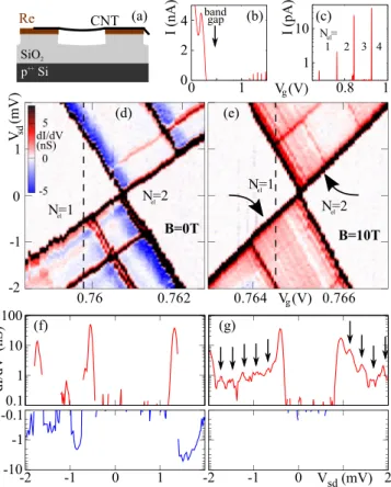
II. CONDUCTION SIDE BANDS AT FINITE FIELD A sketch of the measured device is depicted in Fig. 1(a).
Following Ref. [21], a carbon nanotube is grown over pre- defined rhenium contact electrodes and etched trenches.
Subsequently, the device is cooled down in a top-loading dilution refrigerator and characterized electronically at a base temperature of T mc 30 mK, immersed into the diluted phase of the 3 He / 4 He mixture. The length of the suspended nan- otube segment is L = 700 nm. The device has already been characterized electronically in Refs. [20,22,23]; as can also be seen in the current trace at low bias of Fig. 1(b), it displays the behavior of a small band-gap single-wall carbon nanotube, with transparent hole conduction and strong Coulomb block- ade at low electron numbers. The first Coulomb oscillations exhibit very low current and require particular care to be resolved, see Fig. 1(c). Here, the opaque tunnel barriers are given by p-n junctions extended along the nanotube, between the electrostatically induced n-quantum dot and p-behavior near the leads [24,25].
In the following, we focus on the 1 N el 2 transition,
i.e., the second Coulomb oscillation at the electron side of the
band gap. Figures 1(d) and 1(e) display the stability diagram
close to the corresponding degeneracy point, for (d) B = 0
and for (e) a magnetic field B = 10 T applied in parallel to
the carbon nanotube axis. The overall conductance is very
low; even so, the color scale in the figure has been cut off
such as to focus on the substructure of the single electron
tunneling (SET) regions. The strong black lines, correspond-
ing to electronic excitations, shift with magnetic field; their
detailed behavior, as well as the negative differential con-
ductance at B = 0, is topic of ongoing analysis. The figures
display a clear qualitative difference: While the areas between
the electronic excitation lines are featureless in Fig. 1(d),
in Fig. 1(e) they display a multitude of fine, closely spaced
conductance resonances [see the arrows in Fig. 1(e)]. This also
becomes visible in the comparison of the trace cuts of Fig. 1(f)
(B = 0 T) and Fig. 1(g) (B = 10 T).
0.76 0.762 -2
-1 0 1
0.764 0.766
B=0T B=10T
N=2 N=1
N=2 V (mV)
sdV (V)
g-5
0 5 dI/dV (nS)
Re CNT
p Si SiO
(a)
(d) (e)
(b)
V (V)
g4 2
0 0 1
I (nA) gap
band
1 2 3 4
0.8 1
1 I (pA) 10
(c)
N=1
N =
-2 -1 0 V sd (mV) 2 0.1
1 10 100
-2 -1 0 1
dI/dV (nS)
(f) (g)
-0.1 -1 -10
FIG. 1. (a) Schematic device geometry. A carbon nanotube is grown in situ across predefined rhenium contact electrodes and a trench. (b) Overview device characterization I (V
g) at V
sd= 50 μ V, showing transparent behavior in hole conduction, the band gap, and Coulomb oscillations in electron conduction. (c) Coulomb oscillations I (V
g) for V
sd= 0.5 mV near the band gap, with abso- lute electron numbers N
elmarked. (d), (e) Differential conductance dI / dV
sdat the 1 N
el2 transition, for a magnetic field of (d) B
= 0 and (e) B
= 10 T parallel to the nanotube axis (identical color scale, cut off at + 7 nS for better contrast). (f) Trace dI / dV
sd(V
sd) at B
= 0 T, V
g= 0.7598 V, see dashed line in (d), in logarithmic scale.
The upper panel plots regions of positive dI / dV
sd, the lower panel regions of negative dI/dV
sd. (g) Trace dI /dV
sd(V
sd) at B
= 10 T, V
g= 0 . 7645 V, see dashed line in (e), using the same plotting method and scale as in (f). The equidistant arrows indicate harmonic excita- tion lines.
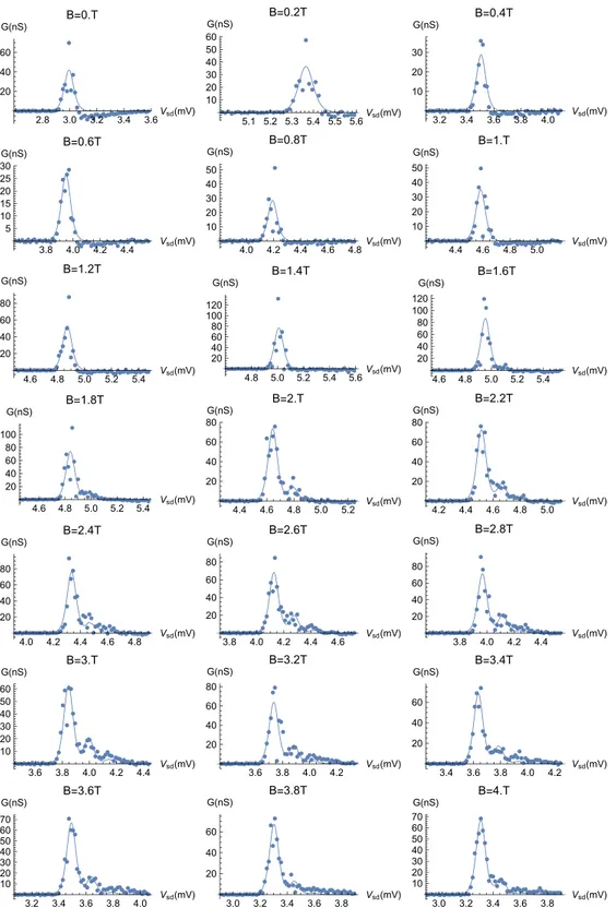
Figure 2(a) demonstrates the emergence of this phe- nomenon with increasing magnetic field. Here, we show the differential conductance dI/dV sd (B ,V sd ) as function of an applied field B parallel to the carbon nanotube axis and of the bias voltage V sd . The gate voltage is kept constant and chosen such that we trace across the N el = 1 edge of the 1 N el 2 SET region, see the inset of Fig. 2(a) for a sketch and Fig. 7(a) in Appendix A for a larger-scale plot of the conductance at the degeneracy point. Here and later, we focus our evaluation on the low magnetic field region since it provides a better signal/noise ratio.
For B = 0, the SET region edge, visible as line of differ- ential conductance, is located at approximately V sd = 0 . 8 mV.
Due to a shift in energy of the electronic states involved in transport, it rapidly moves to higher bias voltages until B 1.5 T is reached. Here, the magnetic field induces a change
-40 0 40 80
N=1 N=2
SET
SET dI/dV (nS)
1 2
1 0 2
0 B (T)
V (mV)
sd5
0 2
4 V (mV)
sdV (mV)
sddI/dV (nS)
2 3
0 60
3
4 6
dI/dV (nS) -20
0 20 40
B (T) (a)
B=3.0T (c)
(b)
(d)
x
zpfx Δx N
N+1
I
thV
sdg=2 (e) g=0
B (T) g (f)
0 0.2 0.4
0 1 2 3 4 5 6 7
FIG. 2. (a) Differential conductance as function of magnetic field parallel to the nanotube axis B
and bias voltage V
sd, dI / dV
sd(B
, V
sd), at constant V
g= 0.7599 V. This cuts through the 1 N
el2 sin- gle electron tunneling region, as sketched in the inset. (b) Similar measurement of dI/dV
sd(B
, V
sd), covering a larger magnetic field range at lower resolution; V
g= 0 . 758 V. (c) Solid line: Smoothened trace dI/dV
sd(V
sd) from (a) at B
= 3 T, displaying the edge of the Coulomb blockade region, corresponding to the 1 N
el2 ground state transition, and conductance side peaks; red points: unfiltered numerical derivative; gray dashed line: fit curve, see the text. (d) Il- lustration of the Franck-Condon coupling mechanism, see the text.
(e) Schematic of the stepwise current increase at increasing bias voltage due to Franck-Condon coupling, here for x = 2x
zpfand thus g = 2 as in (d). (f) Franck-Condon coupling parameter g(B
) as function of the magnetic field; see Appendix B for details of the fit procedure. Red dots: data of (a); blue squares: data of (b).
in ground state, leading to a different energy dispersion.
Soon afterward, sidebands of the differential conductance line emerge, see the arrows in Fig. 2(a). Figure 2(b) displays a larger parameter range than Fig. 2(a), though measured at reduced resolution. Still, the sidebands of the conductance line become clearly visible as an asymmetric broadening of the main conductance line (toward higher bias voltages).
An example trace cut from Fig. 2(a), both smoothened for clarity (black line) and as raw numerical derivative of the current (red points), is shown in Fig. 2(c). A manual analysis of the relative peak positions in each such recorded trace I (V sd ) is given in Appendix A, see, in particular, Fig. 7(f). Its conclusion is that within the scatter the sidebands are equidis- tant within each trace. The excitation energy is magnetic-field independent for B 6 T [26] and given by ε 50 μ eV.
This indicates a harmonic oscillator independent of the elec-
tronic spectrum. Given its energy scale, we can identify it with
the longitudinal vibration of the carbon nanotube [9].
III. FRANCK-CONDON MODEL
In multiple publications, the mechanism leading to vibra- tional harmonic sidebands in transport spectroscopy has been identified as the Franck-Condon principle [4,7,9]. As sketched in Fig. 2(d), the equilibrium position of the vibrational har- monic oscillator depends on the number of charges N el on the nanotube; the rate of SET through its quantum dot is modified by the spatial overlap of the involved harmonic oscilla- tor states | m (N ) | n (N + 1)| 2 = | m (x) | n (x + x)| 2 , with m and n as the vibrational quantum number at N and N + 1 electrons, respectively. x is the displacement of the harmonic oscillator by the additional charge, cf. Fig. 2(d).
The coupling strength is parametrized via the Franck-Condon coupling parameter g = ( x / x zpf ) 2 / 2, comparing x with the characteristic length scale of the harmonic oscillator x zpf =
√ h/mω. ¯
As sketched in Fig. 2(e), a finite value of g leads to a re- distribution of current between vibrational state channels: At the bias voltage corresponding to the bare electronic transition energy, N −→ N + 1 current is suppressed, but it increases whenever an additional vibration state becomes energetically available. A large number of extensions to this model has been developed to take into account specific details of transport spectra, see, e.g., Refs. [8,19,27–42]; however, for now we focus our analysis on the simplest theoretical case, assuming a single harmonic oscillator mode and fast relaxation into the vibrational ground state. In this case, the current step heights or conductance peak amplitudes follow the Poisson formula [4,10], P n = (e − g g n ) / n! , n = 0 , 1 , 2 , . . . , at an en- ergy E vib = n h ¯ ω from the bare electronic-state transition supplied via the bias voltage. The resulting step function of the current, in absence of broadening effects, is sketched in Fig. 2(e) for the example of a large g = 2.
At base temperature, with 25 mK k B 2 μeV, we ex- pect the conductance lines to be lifetime-broadened, with a Lorentzian line shape. Thus, a sum of Lorentzians with ampli- tudes following the Poisson sequence and center points shifted by equidistant bias voltage offsets can be envisioned as model.
In practice, it turns out that the Lorentzian line shape does not suit the measurement data well; this may indicate broadening effects beyond temperature and lifetime, as, e.g., fluctuating gate or bias voltages. Empirically, we choose the resonance shape of thermal broadening, ∝cosh − 2 , instead [43]. Details of the fit procedure can be found in Appendix B.
The result of evaluating the Franck-Condon coupling pa- rameter g for each trace dI / dV sd (V sd ) at fixed B is plotted in Fig. 2(f). It shows the resulting magnetic-field dependence g(B ) for the N el = 1 −→ N el = 2 ground-state transition.
The absence of sidebands for B < 1.5 T corresponds to an absence of coupling, i.e., g ∼ 0. For B 1.5 T, the coupling increases monotonously, reaching a maximum value g(B ) 0.3 at 2.5T B 3 T. Subsequently, we observe a slow decrease and stabilization at g(B ) 0.2.
IV. RELATION TO ELECTRONIC STATES
To our best knowledge, no similar observations of a magnetic-field-dependent electron-vibron coupling have been published so far. Its onset at an anticrossing of electronic
2 2.5 3
4 6
0.5 1 1.5
4 6
0 1 2 3
0 5 10 15
-20 0 20 dI/dV (nS)
(a) (b)
(c)
B (T) V (mV)
sdB (T)
B (T)
V (mV)
sdV (mV)
sd0 20
dI/dV (nS)
4 5 6 7 4 5
(d) (e)
V (mV)
sd2.7T 0.85T
(f)
0 0.2 0.4
0 1 2 3
GS ES
FIG. 3. (a) 1 N
el2 excitation spectrum: Differential con- ductance dI/dV
sd(B
, V
sd) as function of magnetic field B
and bias voltage V
sd, for constant gate voltage V
g= 0 . 7599 V. (b), (c) Detail enlargements (same color scale) of the areas marked with dashed rectangles in (a). (d), (e) Trace cuts dI / dV
sd(V
sd) at the positions indicated in (b) and (c). Conductance peaks with clear vibrational sidebands are shaded. (f) Magnetic-field evolution of the Franck- Condon coupling g(B
) for the excited-state transition marked with arrowheads in (a) (black), compared with the ground-state transition [red dots, same data as in Fig. 2(f)]. For the ground state, the error bars [already shown in Fig. 2(f)] have been omitted for clarity. The solid line is a linear fit after manual removal of outliers.
states, see the dashed ellipsoid in Fig. 2(b), suggests a con- nection to the electronic quantum numbers. As opposed to previous reports on the longitudinal vibration mode [9,13–
15,17,19], here we are characterizing a device where the nan- otube has grown cleanly across pre-existing contacts, and no (accidental or intentional) strongly inhomogeneuous potential distorts the wave functions in the suspended macromolecule away from the metallic contacts [20]. With this in mind, we have analyzed the vibrational sideband behavior of the elec- tronic excited states in the transport spectrum.
A plot of the differential conductance at fixed gate voltage, as function of B and the bias voltage V sd , now over a large bias range, is shown in Fig. 3(a). A preliminary evaluation of the data of Fig. 3(a), taking also into account the one-electron ex- citation spectrum of the device [20], reveals two energetically close shells with both intra- and intershell exchange inter- action [44]; detailed modeling of the two electron transport spectrum will be the topic of a separate work. Here, we limit ourselves to a straightforward classification of conductance lines by magnetic field dispersion; see Appendix C for the details.
The dominant magnetic field dependence of the electron
energies in a carbon nanotube in an axial field originates
from the electronic orbital magnetic moment μ orb , see, e.g.,
Refs. [20,45,46], and Appendix C. Thus, both one- and
two-electron quantum states become at large field angular
0 5 10 15
0 1 2
down up
0 0.2 0.4 0.6 0.8 1
0 1 2
down up
(a) (b)
B
||(T) B
||(T)
V
sdg (mV)
FIG. 4. Evaluation of the conductance resonances in Fig. 3(a) for harmonic sidebands; same data plotted in two different representa- tions: (a) Coupling gas symbol size (downward lines, black triangles;
upward lines, red circles) for the parameter set (B
,V
sd) where it was evaluated, and superimposed on the resonance pattern (background);
(b) coupling g as function of magnetic field B
, irrespective of bias voltage. The solid line is the linear fit of Fig. 3(f).
momentum (and valley) eigenstates, and the slope of a con- ductance line in Fig. 3 indicates the angular momentum change when a second electron tunnels onto the quantum dot.
If the state of the first electron remains unchanged, only the contribution of the second electron to the magnetic moment—
parallel or antiparallel to the magnetic field—determines the magnetic-field dispersion. From this, we can classify the con- ductance lines of Fig. 3(a). As expected, in the low-bias region of the figure, two dominant slopes clearly emerge; we identify these with the addition of a K -valley electron (downward slope) or a K-valley electron (upward slope), respectively [20,45,46].
Figures 3(b) and 3(c) enlarge the regions marked in Fig. 3(a) with dashed rectangles. Also here, the harmonic side- bands are immediately visible. However, at a first glance, only the downsloping spectral lines, where an electron is added in a K -valley state, seem to exhibit electron-vibron coupling. Also the trace cuts at B = 2.70 T [Fig. 3(d)] and B = 0.85 T [Fig. 3(e)] demonstrate this, with the resonances accompanied by sidebands highlighted in green.
Extracting the Franck-Condon coupling parameter g(B ) for an exemplary excited-state resonance [green arrowheads in Fig. 3(a)], using an identical fit procedure as for Fig. 2(f), we compare its evolution over the entire field range 0 T B 3 T with the two-electron ground state transition in Fig. 3(f).
A finite g persists to much lower magnetic field for the excited state transition; indeed, the plot shows a linear growth of g(B ) in this range with g(B ) 0.124 1/TB (gray solid line). The sudden onset of coupling for the ground-state transition is thus consistent with a valley dependence and the change in ground state quantum numbers at B 1.5 T, see the struc- ture marked with a dashed ellipsoid in Fig. 2(b).
We have performed a systematic analysis of the conduc- tance resonances in Fig. 3(a) by dividing them into segments at each crossing or anticrossing and evaluating each segment;
details can be found in Appendix D. The result is shown in Fig. 4. Figure 4(a) displays symbols with their size represent- ing the obtained g parameter, superimposed on the line pattern of Fig. 3(a) at the parameters (B , V g ) where the evaluation has
0.5 1
2 6
V
sd(mV)
-0.08 0 0.08 dI/dV (nS)
B (T) (a)
N=0 N=1 SET
SET
1.5 K'↑
K'↓
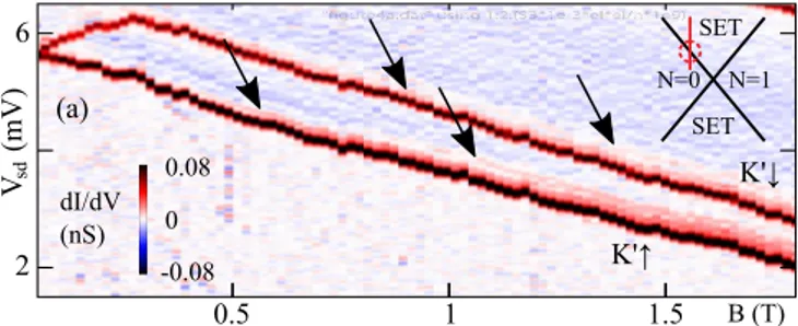
FIG. 5. Magnetic field behavior of the 0 N
el1 one electron ground-state transition. Traces of vibrational sidebands are indicated by arrows. Note that the color scale is cut off at ± 80 pS.
taken place. Figure 4(b) plots the value of g as function of the selected magnetic field, irrespective of bias voltage V sd and thus selected resonance line, with the fit function of Fig. 3(f) added. In both cases, red circles represent downsloping lines, black triangles upsloping lines. The result confirms our visual impression. In general, the upsloping lines, where an electron is added in a K state, display no vibrational sidebands, with the notable exception of the segment at (3 T, 6 mV). The downsloping lines, where an electron is added in a K state, show a g growing with magnetic field, in most cases following the same linear behavior as already observed in Fig. 3(f). One resonance line, also enlarged in Fig. 3(b), deviates with a large g.
It remains to clarify whether the observed effect is specific to the 1 N el 2 region. Figure 5 displays the magnetic- field dependence of a cut across the 0 N el 1 ground-state transition. Also here, where an electron tunnels into a K state of the otherwise unoccupied conduction band, an onset of harmonic sidebands can be visually identified, for both spin alignments. Given the significantly lower conductance here, a more detailed evaluation turns out to be challenging. We can however conclude that the electron-vibron coupling is already inherent to single electron phenomena, and not limited to two-electron states [19]. This indicates a selectivity directly related to the single-particle valley quantum number.
V. DISCUSSION
The transport spectra were measured with the carbon nan- otube immersed into the 3 He / 4 He mixture (D phase) of the dilution refrigerator. Its viscosity at base temperature, η ∼ 10 − 5 N s/m 2 [47], is sufficiently high to mechanically dampen the transversal vibration mode [48]. As observed here, this does not affect the longitudinal mode; a likely explanation is that motion along the nanotube axis does not require any displacement of liquid.
In literature, Weber et al. [19] have reported an electronic
state dependent Franck-Condon coupling in a N el = 4n + 2
quantum dot, switchable via a local gate potential defor-
mation. They apply a magnetic field perpendicular to the
nanotube, and see no effect of that field on the vibrational
sidebands. Due to valley mixing and the field direction, their
data is in the regime of bonding and antibonding valley linear
combinations. A different electron-vibron coupling of (valley-
ground state) spin singlet and (valley-distributed) spin triplet
states, as observed there, obviously can also indicate a valley- dependent effect. Whether this is related to our results still requires further analysis.
Models discussing strong electron-vibron coupling in carbon nanotube quantum dots typically assume an inhomo- geneuous charge distribution relative to the vibration mode envelope, or more generally, a different localization of elec- tron and vibron wave function, see, e.g., Refs. [9,30,32,37].
This is consistent with the occurrence of Franck-Condon sidebands in devices with local gates close to the nanotube [14,18,19]. In previous devices without such an electrode, a local potential may have been introduced via fabrication defects or impurities on the nanotube [9,13,15]. These expla- nations do not lend themselves for the device presented here, displaying a highly regular one electron spectrum [20] and a regular addition spectrum over a large electron number range [22,49]. Nevertheless, the formation of the quantum dot via gate-induced p-n junctions, see, e.g., Refs. [24,25], leads to an electronic confinement more narrow than the mechanically active device length, and typically centered within the sus- pended nanotube segment.
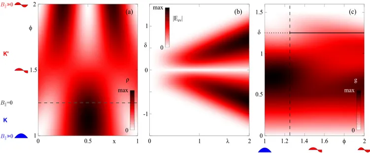
Comparison with existing theoretical [30,37] and exper- imental works [19] then suggests that the axial magnetic field modifies the Franck-Condon coupling g by shifting the electronic wave function relative to the vibron envelope. A valley-dependent mechanism having this effect was recently proposed in Ref. [20], based on Refs. [50–52]. Essentially, the axial magnetic field introduces an Aharonov-Bohm phase around the nanotube. Due to the bipartite graphene lattice, the axial component κ and the circumferential component κ ⊥ of an electron-state wave vector are coupled; one exam- ple solution is plotted in Fig. 6(a) following Ref. [20]. The axial magnetic field thus also modifies the longitudinal bound- ary conditions and thereby the charge distribution along the carbon nanotube axis: the wave-function envelope for each graphene sublattice is tuned from a λ/4 shape, with a finite value at one edge, near B = 0 to a λ/2 shape, as expected for a traditional “quantum box”, at large field; see the drawings in Fig. 6(a).
VI. VARIABLE COUPLING MODEL
Based on the arguments brought forward in the previ- ous section, we have constructed a toy model following Refs. [20,37]. Details can be found in Appendix E; our steps are summarized as follows: we simplify the electronic wave- function amplitudes on the two graphene sublattices to be of the shape ψ ∝ sin(πφx) over the length of the quantum dot, where φ ∈ [1, 2] is used to continuously tune the wave function shape from one antinode to two antinodes and thus approximate the impact of the magnetic field. The total linear charge density ρ(x) is obtained by summing up the charge densities ∝ |ψ| 2 of the sublattices, one being the spatial mir- ror image of the other [20]. The vibron is equally simplified as having a deflection amplitude u(x) ∝ sin(π x).
Given the strong confinement of our electronic states and the low characteristic energy of our harmonic excitations, the quantum dot occupies likely a smaller part of the nanotube than the vibron. Figure 6(b) shows both charge density and vibron envelope for a length ration L d /L v = 1/2 and for a
FIG. 6. Variable coupling model construction. (a) Low-energy wave function solutions for electrons on one of the carbon nanotube sublattices, in the case of hard longitudinal confinement and cross quantization, following Ref. [20]. Solid lines plot the allowed wave vector ( κ
⊥, κ ), schemata the resulting envelope of the sublattice wave function for a K
and a K state. An axial magnetic field modifies the boundary conditions, tuning κ
⊥toward higher values. (b) Exam- ple arrangement of a vibron and a quantum dot. Green line: Vibron amplitude envelope, length L
v= 1. Color plot, charge density of a quantum dot of length L
d= L
v/ 2, summed over both sublattices, as function of position and a parameter φ that tunes the per-sublattice wave function shape from one antinode ( φ = 1) to two antinodes (φ = 2). (c) Approximation for the Franck-Condon parameter g as function of φ and thereby the magnetic field B
, see the text.
shift in center position x d − x v = −0.625 L v . The charge den- sity is plotted as function of both the position and φ, for the range φ ∈ [1.25, 2] approximately covered by a K state when the axial magnetic field is tuned from zero to large values, cf.
Fig. 6(a) and Ref. [20].
Following Ref. [37], we assume the interaction energy between linear charge density and deformation potential to be
E ev ∝
ρ(x) du
dx dx (1)
and the Franck-Condon parameter to be g ∝ |E ev | 2 . The result for g(φ) is plotted in Fig. 6(c), see the red solid line. Recalling that φ = 2 here describes the asymptotic limit of large B , the result qualitatively agrees with the behavior of g for a K state in our experiment, cf. Fig. 3(f) for the low-field and Fig. 2(f) for the high-field behavior. For the same magnetic field range, a K state covers the range φ ∈ [1, 1.25], with the large field limit φ = 1. Here, the coupling further decreases and remains small, see the dotted blue line.
Despite the many simplifications, this model describes the
essential observations of the measurement. For a K state,
the Franck-Condon coupling increases from near zero with
magnetic field, reaches a maximum, and then for large field
becomes constant at smaller value. For a K state, the coupling
remains low. The sudden onset of coupling for the ground
state around B = 2 T, Fig. 2(f), is due to a transition between
these two cases. Limitations of the model become clear, how-
ever, when we look at the size ratio and placement of electron
and vibron. In an ultraclean, suspended nanotube device, we expect the electronic system to be approximately centered in the suspended part. The vibron should cover at least the entire suspended part, which speaks against a spatial arrangement as shown in Fig. 6(b). A parameter search using our toy model has not yielded fundamentally different situations with suitable g(B ) behavior so far. This shall likely require a more realistic and in particular also quantum mechanical treatment.
VII. CONCLUSIONS
In conclusion, we demonstrate that vibrational sidebands emerge in the 0 N el 2 transport spectrum of an ultr- aclean nanotube at a finite magnetic field parallel to the nanotube axis. The sidebands are equidistant, with an oscilla- tor quantum field-independent for B 6 T. Their evaluation results in a field-dependent Franck-Condon coupling parame- ter g(B ). Our data indicate that, predominantly, conductance lines corresponding to the addition of a K valley electron develop a finite coupling parameter g. A tentative mechanism for this can be a field-induced and valley-selective modifica- tion of the electronic wave-function envelope [20]. Following Ref. [37], we have developed a simplified classical model and are able to reproduce the essential behavior of g. A realistic match of device and model parameters will require a more detailed theoretical treatment.
It has long been proposed that, similar to existing exper- iments using the transversal vibration [53], the longitudinal vibration coupling in a carbon nanotube Franck-Condon sys- tem can also be controlled via changing the charge distribution along the nanotube [30,37]. With our experimental results supporting this idea, the integration of the longitudinal vi- bration mode into quantum technological applications and its targeted manipulation as quantum harmonic oscillator [15]
now becomes an interesting challenge.
ACKNOWLEDGMENTS
We would like to thank M. Marga´nska, M. Grifoni, A.
Donarini, Ch. Strunk, E. A. Laird, and P. Hakonen for in- sightful discussions, and Ch. Strunk and D. Weiss for the use of experimental facilities. The data has been recorded using the L AB ::M EASUREMENT software package [54]. The authors acknowledge financial support by the Deutsche Forschungs- gemeinschaft (Emmy Noether Grant Hu 1808 / 1, GRK 1570, SFB 689, and SFB 1277) and by the Studienstiftung des deutschen Volkes.
The device was fabricated by P.L.S. and D.R.S; the low- temperature measurements were performed by all authors jointly. The resulting data was evaluated by P.L.S. and A.K.H.;
the paper was written and the project was supervised by A.K.H.
APPENDIX A: HARMONICITY AND EXCITATION ENERGY
Figures 7(a) and 7(b) display the conductance near the 1 N el 2 degeneracy point, for B = 0 T and B = 5 T and over a large bias voltage range |V sd | 10 mV. The mag- netic field dependent measurements evaluated in Figs. 2 and 3
correspond to traces taken across the SET region, in the pa- rameter range indicated in Fig. 7(a) by a yellow marker. Part of such a trace dI / dV sd (V sd ) for constant B and V g is shown schematically in Fig. 7(c). From it, the peak distances V sd1 , V sd2 , V sd3 as indicated in the drawing can be extracted.
They correspond to excitation energies ε 1 , ε 2 , ε 3 . In the stability diagrams, conductance lines ending at the N el = 2 Coulomb blockade region (i.e., for V sd > 0 with negative slope) correspond to two-electron excitations; lines ending at the N el = 1 Coulomb blockade region (i.e., for V sd > 0 with negative slope) correspond to one-electron ex- citations. In the evaluated parameter region, only lines with negative slope are visible. For them, the conversion from bias voltage distances V sd to excitation energies ε, based on the capacitances in the quantum dot system, can be illustrated by the sketch of Fig. 7(b). Given the slopes V sd /V g of the two edges of the SET region in the stability diagram, s 1 < 0 and s 2 > 0, as indicated in the sketch, the conversion factor
f (B , V g ) can be derived from elementary geometry as
ε = 1
1 − (s 1 / s 2 ) e V sd = f (B ,V g ) e V sd . (A1) Here we indicate with f (B ,V g ) that the factor can change with magnetic field and gate voltage due to modification of the electronic wave function shapes and thus the charge dis- tributions and capacitances. The value of f , as extracted from stability diagrams at B = 0, 5, 10 T, is plotted in Fig. 7(c), with a linear fit added. In the plotted range, f varies by only approximately 10%.
The result of a manual evaluation of the data of Fig. 2(b), where peak positions have been read out from line plots, is shown in Fig. 7(d). Here, the red squares correspond to the peak distance of the first sideband relative to the base conductance resonance, the black dots to the one of the second sideband relative to the first sideband, and the blue triangles to the one of the third sideband relative to the second sideband.
The left axis displays distance in bias voltage, the right axis the value converted into energy, using constant f (5 T) for simplicity. Within the scatter, the three types of points lie in the same band of values, indicating equidistant quantum states and thus harmonic oscillator behavior. The oscillator quantum is for 0 T B 6 T approximately constant at V sd 0.15 mV, corresponding to ε = hω ¯ 50 μeV; this is the region predominantly discussed in the main text.
For larger B , the data points seem to indicate a gradual increase in ε. Given the decreasing signal-to-noise ratio and limited data for this field range, it is unclear whether this is a real effect. Surprisingly, the stability diagram at B = 10 T, Fig. 1(e), displays V sd 0.25 mV, which would confirm such an increase.
The theoretical value for the energy quantum of the carbon nanotube longitudinal vibration is given by [9]
ε th = h L
Y
ρ , (A2)
where L is the nanotube length, Y is Young’s modulus, and
ρ is the nanotube mass density. Assuming ρ = 1.3 g/cm 3 and
V (mV)
sddI/dV(ns)
2 3
0 60
ΔV
sd3ΔV
sd2ΔV
sd1ΔV
sdΔε/e
s1 s2
V
sdV
g(c)
(d)
(e)
0.3 0.32 0.34 0.36
0 5 10
magnetic field (T)
f ener gy (meV)
0.1 0.2
magnetic field (T)
0 2 4 6 8 10
0.02 0.04 0.06
distance 1 distance 2 distance 3 (f)
V (mV) V
sdV V V
dI/dV(ns)
2 3
0 60
ΔV V V
sd3ΔV
sd2sΔV
sd1sΔV
sdsΔε/e
s1 s2
V
sdVV V
V
gV V V V (c)
(d)
(e)
0.3 0.32 0.34 0.36
0 5 10
magnetic field (T)
f en er gy (meV )
0.1 0.2
magnetic field (T)
0 2 4 6 8 10
0.02 0.04 0.06
distance 1 distance 2 distance 3 (f)
0.755 0.76 0.765
-10 -5 0 5 10
0.755 0.76 0.765
-40 -20 0 20 40 60
(a) (b)
B=0T B=5T
V (mV)
sdV (V) g N=1
V (mV)
sdN=1
dI dV (nS)
N=2 N=2
N=1 N=2
FIG. 7. (a) Large bias voltage range stability diagram dI / dV
sd(V
g, V
sd) of the 1 N
el2 transition at B
= 0 T. Figure 1(d) is a detail zoom of this plot. The parameter region of the trace cuts evaluated in Figs. 2 and 3 is shaded in yellow. (b) Large bias voltage range stability diagram dI/dV
sd(V
g, V
sd) at B
= 5 T. (c) Illustrative example trace dI /dV
sd(V
sd) for constant B
and V
g. (d) Using the slopes V
sd/V
gof the two edges of the single electron tunneling region in the stability diagram, s
1< 0 and s
2> 0, the bias differences V
sdcan be converted to energy differences ε (here demonstrated for a N
el= 2 state). (e) Conversion factor f (B
), defined via ε = f (B
) · eV
sd, as extracted from the stability diagrams at B
= 0 T [see (a), Fig. 1(d)], B
= 5 T [see (b)], and B
= 10 T [see Fig. 1(e)]. (f) Manually extracted distances between conductance peak positions, cf. (a), using the data set of Fig. 2(b). Left axis: Raw distances in bias voltage, right axis: distances converted to energy, using f (5 T).
Y = 1 TPa, this results in [9]
ε th ≈ 0.11 meV
L(μm) . (A3)
For our device, using the contact separation of L = 0 . 7 μ m as approximate value of the suspended nanotube segment length, we obtain ε th 160 μeV. While there is a clear deviation, our measurement still lies at the edge of the typical scatter of oscillator quanta observed in experimental literature, see Fig. 8 for an overview.
APPENDIX B: FRANCK-CONDON MODEL AND FIT PROCEDURE
In the context of SET through a carbon nanotube, the Franck-Condon coupling parameter g describes the spatial
shift of the nanotube equilibrium position as harmonic oscil- lator when an additional electron is added to it. It is given by g = ( x 0 / x zpf ) 2 / 2, where x 0 is the shift in equilibrium po- sition, x 0 = x 0 (N + 1) − x 0 (N ). In the denominator, x zpf =
√ h/(mω) is the characteristic length scale of the harmonic os- ¯ cillator, describing the wave function extension of the ground state and/or its zero point fluctuations. For ¯ hω = 50 μeV and m = 1 . 3 × 10 −21 kg [55], we obtain x zpf = 1 . 0 pm.
At finite temperature, a harmonic oscillator can both absorb
and emit vibrons. Here, in the limit of low temperature and
fast vibrational relaxation compared to the tunnel rates, we
assume that for any SET process we start out in the N el elec-
tron vibrational ground state. For each number of vibration
quanta n, there is a distinct overlap | 0 (N el ) | n (N el + 1)| 2
of the N el electron vibrational ground state with an N el + 1
electron, n vibron state. This leads to a series of equidistant
steps in current I(V sd ) or peaks in differential conductance
0.01 0.1 1 10 100
0 500 1000 1500
energy (meV)
Length (nm)
theory Sapmaz et al, PRL (2006) Hüttel et al, NJP (2008) Hüttel et al, PRL (2009) Leturcq et al, Nat. Phys. (2009) Island et al, Nano Lett. (2012) Ganzhorn et al, Nat. Nano. (2013) Jung et al, Nano Lett. (2013) Weber et al, Nano Lett. (2015) this work
0.1 1 10 100
10 100 1000
relative energy (1)
Length (nm)
theory Sapmaz et al, PRL (2006) Hüttel et al, NJP (2008) Hüttel et al, PRL (2009) Leturcq et al, Nat. Phys. (2009) Island et al, Nano Lett. (2012) Ganzhorn et al, Nat. Nano. (2013) Jung et al, Nano Lett. (2013) Weber et al, Nano Lett. (2015) this work
FIG. 8. Overview of carbon nanotube longitudinal vibration oscillator quanta ε = h ¯ ω observed in published literature [9,13–19] as function of device length, in comparison with the theoretical result ε
th(L) = 110 meV / L[nm]. Left: Unscaled ε (L), linear length scale;
right: ε(L)/ε
th(L ), logarithmic length scale.
dI /dV sd (V sd ), whenever sufficient energy for reaching the next vibrational state becomes available.
The contributions of the vibrational states and thus the current step heights are given for the limit of low temperature and fast vibrational relaxation by the Poisson formula [4,10],
I n ∝ e − g g n
n! , n = 0 , 1 , 2 , . . . (B1) at an energy ε = n hω ¯ from the bare electronic state transition.
The resulting step function of the current, in the idealized case of total absence of effects such as thermal or lifetime broadening, is shown in Figs. 9(a)–9(c) for different values of g.
In a measurement, the steps will be broadened due to finite temperature, finite lifetime of the involved quantum states, and additional mechanisms such as, e.g., potential fluctua- tions. As an approximation, we assume that this broadening equally affects all steps. Then, the differential conductance G = dI/dV sd exhibits a sequence of peaks, each correspond- ing to one step in current, with conductance peak heights proportional to the current step heights. Even though G is in our measurement a derived quantity, it is both a better base for visualization of the phenomena, see the figures of this paper, and a better base for numerical curve fitting than the measured current. To minimize the impact of postprocessing, we use for the fits the raw numerically differentiated conductance I / V sd , without any smoothing or other numerical filtering applied.
As already mentioned in the main text, we find that our data is fitted well using the typical shape of a thermally broadened
Coulomb oscillation, G th
V sd , V sd 0
=
cosh
V sd − V sd 0 γ
−2
, (B2) where γ describes the peak width. For our fit model, we sum up a sequence of these peaks, weighted according to Eq. (B1),
~ V
sd~ V
sd~ V
sd1
0
g=0.2 g=1 g=5
I / I
maxΔV correspon- ding to Δε=ħω
sd


![FIG. 8. Overview of carbon nanotube longitudinal vibration oscillator quanta ε = h ¯ ω observed in published literature [9,13–19] as function of device length, in comparison with the theoretical result ε th (L) = 110 meV / L[nm]](https://thumb-eu.123doks.com/thumbv2/1library_info/3734032.1508838/8.884.160.721.100.523/overview-longitudinal-vibration-oscillator-published-literature-comparison-theoretical.webp)