Research Collection
Doctoral Thesis
Ab initio Quantum Transport in Conductive Bridging Random Access Memory
Author(s):
Ducry, Fabian Publication Date:
2021
Permanent Link:
https://doi.org/10.3929/ethz-b-000474598
Rights / License:
In Copyright - Non-Commercial Use Permitted
This page was generated automatically upon download from the ETH Zurich Research Collection. For more information please consult the Terms of use.
ETH Library
DISS. ETH NO. 27345
AB INITIO QUANTUM TRANSPORT IN CONDUCTIVE BRIDGING
RANDOM ACCESS MEMORY
A thesis submitted to attain the degree of DOCTOR OF SCIENCES of ETH ZURICH
(Dr. sc. ETH Zurich)
presented by FABIAN DUCRY MSc EEIT, ETH Zurich born on 6 November 1988 citizen of Zurich, Switzerland
accepted on the recommendation of Prof. Dr. Mathieu Luisier, examiner Prof. Dr. Alexander Shluger, co-examiner
2021
Contents
Contents iii
Acknowledgments v
Abstract vii
Zusammenfassung ix
1 Introduction 1
1.1 Current Memory Landscape . . . 1
1.2 Conductive Bridging RAM . . . 4
1.2.1 Working Principle . . . 6
1.2.2 Modeling of CBRAM . . . 10
1.3 Motivation and Objective of the Thesis . . . 14
1.4 Outline of the Thesis . . . 15
2 Quantum Transport from First Principles 17 2.1 Introduction . . . 17
2.2 Density-functional Theory . . . 18
2.2.1 Molecular Dynamics . . . 24
2.3 Quantum Transport . . . 26
2.3.1 Electron Transport . . . 27
2.3.2 Thermal Transport . . . 37
2.3.3 Electro-thermal Coupling . . . 40
2.4 Mode-Space Approximation . . . 46
3 Application of the Mode-Space Approximation to CBRAM Cells 53 3.1 Introduction . . . 53
3.2 Atomic Device Structure . . . 55 iii
3.3 Parameterization of the Equivalent Model . . . 55
3.4 Hybrid mode-space – real-space device Hamiltonian . . . 63
3.5 Ballistic Simulations: Benchmark . . . 66
3.6 Conclusion . . . 68
4 Filament in a Cu/a-SiO2/Cu Cell 71 4.1 Introduction . . . 71
4.2 Computational Details . . . 73
4.3 Results . . . 77
4.3.1 ON-Off Switching . . . 77
4.3.2 Electro-thermal Properties of the CBRAM in ON- state . . . 81
4.3.3 Influence of the Oxide Thickness on Self-Heating . 86 4.4 Conclusion . . . 88
5 Impact of the Counter Electrode Metal in Ag/SiO2/M Cells 91 5.1 Introduction . . . 91
5.2 Computational Details . . . 93
5.3 Results . . . 97
5.4 Conclusion . . . 100
6 Conclusion and Outlook 101 6.1 Summary . . . 101
6.2 Outlook . . . 102
References 107
List of Publications 135
Curriculum Vitae 139
Acknowledgments
Foremost I would like to express my gratitude to Prof. Dr. Mathieu Luisier for supervising my PhD project and giving me the opportunity to work on this fascinating research topic. I highly value his support and advice and the freedom I was given in pursuing my work. I would also like to thank Prof. Dr. Alexander Shluger for accepting to be the co-examiner of my thesis.
I thank Prof. Dr. Jürg Leuthold and Prof. Dr. Thomas Schimmel for the productive collaboration and discussions. This is extended to all members of this research effort as part of the Werner Siemens Stiftung Center for Single Atom Electronics and Photonics, namely Dr. Alexandros Emboras, Dr. Ueli Koch, Dr. Roland Gröger, Dr. Stefan Walheim, Dr.
Florian Wertz, Dr. Fangqing Xie, Jan Äschlimann, Bojun Cheng, Mila Lewerenz, Elias Passerini, Torben Staiger, and Samuel Zumtaugwald.
I am grateful to the people of the Nano-TCAD group for the pleas- ant atmosphere, inspiring discussions, and encouragement, in particular Cedric Klinkert, Dr. Dominik Bauer and Dr. Tarun Agarwal. I greatly enjoyed working with all of you.
Furthermore, I would like to thank Christine Haller for handling ad- ministrative matters as well as Christoph Wicki, Frank K. Gürkaynak, and Adam Feigin for keeping the IT-infrastructure running and dealing with all my problems and requests.
Finally, I am deeply grateful to my family, to my parents, Esther and Andre, for all their support throughout my life, to my sister Jasmin, and to Theresa. Without her encouragement and support this thesis would not have been possible.
v
Abstract
In line with the growing popularity of data-driven IT applications, the im- portance of data storage and memory has not stopped increasing during the last decade. However, the complementary metal-oxide-semiconductor (CMOS)-based storage and memory technology is reaching its scaling lim- its and has become ill-suited for low power and energy efficient operations.
Therefore, new nonvolatile memory technologies are being developed and are slowly entering the mass market. Among those, conductive bridging random access memory (CBRAM) cells promise great advances in terms of power consumption, integration density, and cointegration with CMOS- based logic circuits. CBRAMs are metal-insulator-metal heterojunctions through which a metallic filament grows and dissolves, which creates two distinctive resistance states corresponding to logical 1 or 0. Nevertheless, several challenges remain to be addressed before they can compete with traditional technologies, particularly with respect to variability and reli- ability. Solving these issues is complicated by the fact that the operating mechanisms of CBRAMs are not fully understood.
The aim of this thesis was to use quantum transport simulations to elucidate the switching characteristics of CBRAM cells. We used density- functional theory to compute the electronic structure of nanoscale com- ponents, from which structural, electrical, thermal and electro-thermal properties of memory cells were derived in a parameter-free manner.
First, the theoretical foundation of first principles-based quantum transport is presented. Such simulation techniques induce an immense computational burden when applied to large models such as CBRAM.
This challenge is assessed and addressed in the subsequent chapters. For that purpose, the so-called mode-space approximation originally derived within the effective mass context was generalized and applied to CBRAM systems. Moreover, the process of obtaining the required mode-space
vii
transformation matrix was largely automatized which drastically simpli- fies the usage of this approach. Its strength and reliability is demonstrated with the help of a CBRAM configuration whose electrical current was computed both with and without the mode-space approximation. We found that the discrepancy between both models can be kept below 2%.
Furthermore, the reduction of the required computational resources was evaluated and we observed that it can be as large as two to three orders of magnitude, depending on the targeted accuracy.
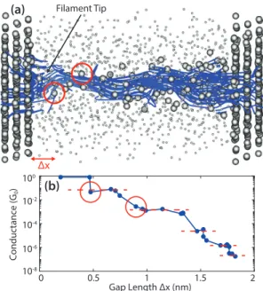
Next, a model for a Cu/SiO2/Cu CBRAM cell is presented. Its ON- OFF switching behavior was investigated and an estimate of the number of atoms that contribute to the process is provided. Multiple intermediate states were simulated to present the electrical conductance as a function of the number of “dissolved” atoms. The results qualitatively agree with experimental data. Moreover, the electro-thermal properties for CBRAM cells of varying size were determined, leading to an explanation for the experimentally discovered improved performance of ultra-scaled devices.
Bringing the memory cell closer to their ballistic transport limit by de- creasing their thickness minimizes the interaction between electrons and atomic lattice vibrations. This in turn lowers the lattice temperature within the cell, thereby improving its thermal stability.
In the last chapter of this thesis, the impact of the CBRAM material stack on the electrical current is examined. We observed that for a given atomic configuration of the filamentary structure in the ON-state, the metal of the counter electrode has little influence on the conductance.
However, the current density is affected by the choice of the electrode material. This fact is likely due to the asymmetric configuration of typical CBRAM cells, which is challenging to account for inab initioquantum transport. However, to assess the resistance state of a filament, a we found that assuming symmetric metallic electrodes is sufficient. Yet, cal- culating further properties of the system such as the interaction with the surrounding oxide, requires representing the full asymmetric nature of CBRAM stacks.
Zusammenfassung
Die zunehmende Beliebtheit von datengestützten Programmen hat die Bedeutung von Datenspeicherung im letzten Jahrzehnt weiter gesteigert.
Die Optimierung von Speicherechnologien welche auf komplementären Metall-Oxid-Halbleitern (CMOS) basieren, nähert sich hingegen funda- mentalen physikalischen Grenzen. Dadurch eignet sich diese Technologie immer weniger für energiesparende elektronische Speicherkomponenten.
Aus diesen Gründen etablieren sich langsam Alternativen zu den her- kömmlichen Speicherelementen. Unter diesen neuen, nichtflüchtigen Da- tenspeichern (NVRAM) verspricht vor allem conductive bridging random access memory (CBRAM) grosse Fortschritte in Bezug auf z.B. Energie- verbrauch und Integrationsdichte. CBRAMs sind Metall/Isolator/Metall Heteroübergänge, in welchen metallische Filamente wachsen und sich auf- lösen. Die An- oder Abwesenheit einer leitenden, metallischen Verbindung zwischen den Elektroden erzeugt unterschiedliche Widerstandszustände.
Damit können die logischen Zustände 1 oder 0 kodieren werden. Um jedoch mit herkömmlichen CMOS-Technologien konkurrenzfähig zu wer- den, müssen mehrere verbleibendende Schwierigkeiten in Bezug auf Varia- bilität und Zuverlässigkeit von CBRAM beseitigt werden. Das Ausmerzen dieser Probleme wird jedoch dadurch erschwert, dass die Funktionsweise von CBRAM nicht im Detail geklärt ist.
Das Ziel dieser Arbeit war es, mit Quantentransport-Simulationen Erkenntnisse über die Funktionsweise von CBRAM zu gewinnen. Dich- tefunktionaltheorie ist ein verbreitetes Verfahren um die elektronische Struktur von Nanokomponenten parameterfrei zu bestimmen. Basierend auf diesen Resultaten konnten strukturelle, elektrische und thermische Eigenschaften von CBRAM-Zellen abgeleitet werden.
Zuerst werden die theoretischen Grundlagen von ab initio Quanten- transport präsentiert. Solche Simulationen verursachen einen erheblichen
ix
Rechenaufwand, wenn sie auf grosse Modelle wie zum Beispiel CBRAM angewendet werden. Dies wird im darauffolgenden Kapitel untersucht und angegangen. Dazu wird die mode-space (MS) Methode verallgemei- nert um sie auf CBRAM-Systeme anwenden zu können. Zudem wurde der Prozess um die dazu benötigte Transformationsmatrix zu berechnen weitgehend automatisiert, was die Anwendung der Methode erheblich ver- einfacht. Die Vorteile und Zuverlässigkeit der Methode wurde anhand des Modells einer CBRAM-Zelle untersucht, indem der elektrische Strom mit und ohne MS-Methode berechnet wurde. Wir sahen, dass die Abweichun- gen im Resultat unter 2% gehalten werden konnten. Des Weiteren eru- ierten wir, wie viele Ressourcen mit der MS-Methode eingespart werden konnten und ermittelten eine Reduktion um 2 bis 3 Grössenordnungen, je nach angestrebter Genauigkeit.
Danach wird das Modell einer Cu/SiO2/Cu CBRAM-Zelle präsen- tiert. Deren Abschaltvorgang wurde untersucht und eine Abschätzung zur Anzahl Atome die dazu bewegt werden müssen wird gegeben. Mehrere Widerstandszustände zwischen dem Ein- und dem Auszustand wurden simuliert um die Leitfähigkeit als Funktion der Anzahl der diffundier- ten Atome zu berechnen. Die Resultate stimmen qualitativ mit expe- rimentellen Untersuchungen überein. Zudem wurden elektrothermische Eigenschaften von CBRAM-Zellen verschiedener Grössen bestimmt. Die- se Resultate zeigten auf, warum das Verkleinern der Speicherzellen deren Zuverlässigkeit verbessern kann. Je dünner das Speicherelement ist, je weniger interagieren die Elektronen mit den Atomen im Kristallgitter im Herzen des Speichers und geben entsprechen weniger Energie in Form von Wärme an dieses ab. Dies verringert die Betriebstemperatur des Speichers und erhöht damit die thermische Stabilität.
Im letzten Kapitel dieser Arbeit wird der Einfluss der Materialzusam- mensetzung auf den elektrischen Strom untersucht. Bei einer vorgegebe- nen Form der atomaren Struktur des Metallfilaments hatte die Wahl des Materials der Elektrode einen vernachlässigbaren Einfluss auf die Leitfä- higkeit der Speicherzelle im eingeschalteten Zustand. Deren Stromdichte
Zusammenfassung xi hingegen wurde stark vom Metall beeinflusst. Diese asymmetrische Kon- figuration von CBRAM-Zellen ist jedoch schwierig in ab initio Simulatio- nen aufzunehmen. Um nur den Widerstand eines Filaments zu ermitteln, eignen sich daher vereinfachte symmetrische Modelle. Für weitergehende Untersuchungen hingegen, muss diese Vereinfachung aufgegeben werden und der asymmetrische Charakter vom CBRAM-Zellen berücksichtigt werden.
Chapter 1
Introduction
1.1 Current Memory Landscape
Data storage is a fundamental component of any information processing system. Present-day memories are based on the complementary metal- oxide-semiconductor (CMOS) technology, e.g. static random-access mem- ory (SRAM), dynamic random-access memory (DRAM), or Flash cells.
Because of the different capabilities of these technologies with respect to speed, latency, storage density, and cost, computing architectures rely on hierarchical storage systems. High-density and low-cost Flash drives provide permanent long-term storage, but they are slow to access. DRAM and SRAM units implement temporary, volatile memory, which is faster to access, but at the expense of storage density and cost. The access latency and memory bandwidth limit the data transfer between the stor- age hierarchy levels and create a speed gap between the storage and computing units. This is known as the so-called “memory wall,” which represents a major bottleneck in the current computing architectures [1, 2]. Moreover, the increasing demand for portable electronic devices pow- ered by low-capacity batteries imposes additional hardware requirements.
Altogether, these issues have led to a shift of the focus of the semiconduc- tor industry towards low power computing solutions, although they are challenging to implement with CMOS-based memories. Finally, downscal- ing the feature size of CMOS components has brought this technology close to its fundamental physical limits, hampering further performance
1
improvements and its cost effectiveness [3].
The limitations encountered by traditional memory implementations have sparked intense research interest for alternative technologies that could complement or replace CMOS-based components. These alterna- tive technologies are collectively termed emerging nonvolatile memories (NVM) [4,5]. Of particular interest is the concept of storage class mem- ory (SCM), which combines the advantages of low-cost and high density Flash memories with those of fast and low access latency SRAM cells, while offering low power operations. Promising candidates as emerging NVMs for SCM applications include both types of resistive random-access memories (ReRAMs) [6]. To store data, ReRAM relies on the reversible resistance changes of a soft breakdown in a dielectric layer induced by electrochemical effects [7]. This type of NVM cells can be further divided into two categories: valence change memories (VCM) and conductive bridging random access memories (CBRAM), which are at the core of this thesis. ReRAM memory cells can be scaled down to sub-10 nm sizes while keeping long retention times [8], and can be densely integrated [9].
Such memory cells feature other desirable properties, e.g. high erase-write endurances and window margins [10], low operating energies [11], and sub-nanosecond switching speeds [12,13]. It is, however, important to note that some of these properties have conflicting design requirements such that not all of them can be simultaneously implemented within the same storage unit [14, 15]. Thus, engineering a ReRAM array satisfy- ing all requirements of SCM and being competitive with CMOS-based solutions remains to be demonstrated [6].
A resistive switching behavior has been shown in a large number of material stacks [16]. Each individual configuration comes with its own characteristics such as switching speed, retention time, or turn-on voltage. A huge design space must be explored to obtain a memory cell that optimally fulfills specific application requirements. Moreover, not all aspects of the operating mechanisms in ReRAM are quantitatively understood, the origin of certain effects still being debated [17,18]. An in-
1.1 Current Memory Landscape 3 depth comprehension of the underlying physics is one of the key challenges to address in ReRAM research as it could critically enhance the reliability of these memory cells [19]. Device modeling and computer-aided design can provide valuable insights into the processes governing the ReRAM operation and thereby support on-going experimental activities [20].
An accurate modeling of ReRAMs must cover an enormous time scale and spatial extent. The ON-OFF switching typically occurs within nanoseconds or less and relies on the relocations of single atoms, which can happen within picoseconds. At the same time, the retention capabilities of NVM is measured in years and a memory array is composed of billions of individual cells extending over mm square surfaces. Since no modeling technique can span the enormous time and spatial ranges needed to fully describe ReRAM memory arrays, multiscale approaches are required [20].
Ab initio calculations form an integral part of such approaches due to their ability to model atomistic systems in a parameter-free manner. The majority ofab initiostudies dedicated to ReRAMs focuses on the extrac- tion of relevant physical quantities such as formation energies or diffusion barriers that are used to parameterize macroscopic simulation approaches.
On the other hand, the electrical properties of the nanostructures at the core of ReRAMs have attracted little attention [21].
Modeling ReRAM memory cells faces several challenges because they feature complex filamentary structures and material interfaces. For ex- ample, the discrete properties of the switching layer play a prominent role. Moreover, there is ample evidence that the atomic configuration of ReRAM memory cells changes from cycle-to-cycle, which creates atomic- scale variability and manifests itself in fluctuations in the resistance measured across the memory cell [22]. Controlling these variations is of paramount importance to implement reliable memories. Therefore, atom- istic methods that are able to capture these characteristics should be employed. Another consequence of the atomic scale operation of ReRAM is that electron transport has entered the mesoscopic regime where classi- cal models such as the drift-diffusion equations [23] fail to capture the full
range of the physics at play: quantum mechanical phenomena, e.g. energy quantization, confinement, or tunneling must be taken into account [24].
The presence of quantum mechanical and atomic-scale effects call for an ab initio treatment of ReRAMs. Such methods are directly derived from
physical principles and thus do not require any input parameters.
The ground-state electronic structure of CBRAM cells can be obtained from density-functional theory (DFT) [25, 26], which is a widespread tool to perform ab initio calculations. Out-of-equilibrium properties, e.g. electrical and thermal currents, can be computed using the Non-equilibrium Green’s Function (NEGF) formalism [27,28]. The latter allows for the extraction of transport properties under an external applied bias. Even though ultra-scaled devices operate close to their ballistic limit, many experimental features can only be explained by simultaneously accounting for electrical and thermal effects. This is the case of self-heating, which may be responsible for CBRAM failures at high current densities [29]. Coupled together, DFT and NEGF compose a versatileab initioquantum transport (QT) simulation framework [30, 31].
1.2 Conductive Bridging RAM
CBRAM is a (non)volatile memory technology that stores data through a reversible change in the resistance of a dielectric switching layer (SL).
The SL is embedded between an oxidizable metal and an electrochem- ically inert electrode. The lowering of the resistance is induced by the growth of one or several metallic filament(s) through the SL. Resistive switching was first shown with a VCM-type device using titanium oxide as SL in 1968 [32]. In 1976, Y. Hirose et al. demonstrated a CBRAM-like memory effect in a metal-insulator-metal (MIM) stack by growing Ag dendrites through a layer of As2S3[33]. The first use of this effect in inte- grated circuits occurred twenty years later when Swaroop et al. replaced
1.2 Conductive Bridging RAM 5 analogue CMOS components with CBRAM cells to fabricate artificial solid-state synapses [34]. The first implementation of a vertical CBRAM for memory applications was demonstrated in 1999 by Kozicki et al. us- ing Ag and Cu dendrite growth in As2S3 and GeSe2, respectively [35].
This finding made the CBRAM technology an appealing candidate for data storage in integrated circuits. In 2008, ReRAM cells in general were linked to the theoretical concept of memristor [36], which is an electrical two-terminal component whose resistance depends on the history of the current that flew through it. The memristor is a mathematical construct first hypothesized in 1971 by L. Chua [37].
CBRAMs possess numerous advantages over CMOS-based memory technologies such as Flash, DRAM, and SRAM. First, the resistance state of CBRAM cells can be switched on sub-nanosecond time scales, enabling high speed SET and RESET operations [13]. Second, the ratio between the ON- and OFF-state can typically reach several orders of magnitudes and may reach more than 107 [38]. Third, the size of CBRAM can be scaled down to 10 nm2 areas [39]. Fourth, the relatively simple MIM structure of CBRAM paves the way for high density arrays that can potentially be stacked on top of each other to form 3D structures [40,41].
Fifth, CBRAM can be operated at low voltages, which is favorable for low power applications [29]. Sixth, the memory state can be retained for long times [42]. Last, CBRAM can be constructed solely of CMOS-compatible materials and directly integrated into standard CMOS processes during the back end of line (BEOL) [43]. Despite these benefits, CBRAM re- mains an experimental technology and a niche product from an industrial perspective. This is mainly due to the fact that low power and high speed are usually in competition with reliability and retention times, forcing design engineers to make compromises regarding the aspects that should be favored [14,15]. Nevertheless, in 2014, a chip relying on the CBRAM technology with 16 GB storage capacity was built [44] and the feasibility of automotive grade CBRAM was suggested in 2018 [45].
In addition to electrical operation, the resistance state of CBRAM can
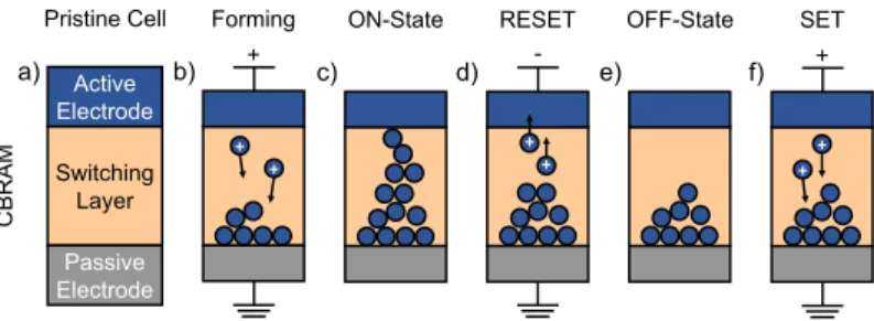
Forming
Pristine Cell ON-State RESET OFF-State SET
Switching Layer Active Electrode
Passive Electrode a)
CBRAM
b) + c) d) - e) f) +
+ +
+
+ +
+
Figure 1.1:Illustration of the bipolar filamentary type switch- ing process in a CBRAM cell. The underlying structure is built of an active electrode (often Ag or Cu), an insulating switch- ing layer (e.g. a-SiO2), and an inert metal electrode (a). The application of a forward voltage oxidizes metal atoms at the interface of the active electrode. These ions migrate towards the passive electrode where they are reduced (b). Eventually, a stable metallic filament is formed that bridges the switching layer (c). By reversing the voltage polarity, the filament can be disrupted (d). Finally, the OFF-state with a partial filament left in the oxide layer is reached (e). The subsequent SET process (f) brings the CBRAM cell back to its ON-state (c). Adapted
from [50].
also be read or set by other physical stimuli. For example, a CBRAM cell can be coupled to optical signals by inserting it into a plasmonic cavity, enabling the optical readout of the memory state of the cell [46]. Further- more, CBRAM cells can function as an electro-optical modulator [47] or detector [48]. Besides memory applications, CBRAMs are investigated as active building blocks of neuromorphic circuits, a potential application currently receiving a lot of attention [49]. While the focus of this thesis lies on memory applications, the presented models and simulations apply to CBRAM cells irrespective of their purpose.
1.2.1 Working Principle
The memory effect in CBRAM is the consequence of a reversible change in the resistance of the SL [7]. In the simplest picture, CBRAM cells are
1.2 Conductive Bridging RAM 7 two-terminal MIM stacks, with the central dielectric acting as the SL, as shown in Fig.1.1(a). In contrast to capacitors, which share the same MIM configuration, the dielectric medium changes its resistance upon application of an appropriate voltage between the two electrodes. In the pristine high-resistance state, called OFF-state, the dielectric behaves as an insulator separating the metallic contacts. The low-resistance ON- state is characterized by a soft breakdown of the insulator through the presence of a metallic filament that connects and thereby short-circuits the two electrodes. Multilevel cells can be realized by carefully controlling the length and thickness of the filament [51]. Consequently, the resistance state of the SL, and thus the memory cell, can exhibit different values.
The reversible breakdown of the SL is illustrated in Fig.1.1(b-f). It is caused by the growth and dissolution of a metallic filament composed of few atoms and extending from one of the electrodes towards the other [52]. Reliable operations require an asymmetric MIM configuration in which the active electrode (AE) is composed of an electrochemically active metal. This chemical species can diffuse into and out of the SL, thus creating the desired ON-OFF resistance switching. The counter electrode (CE) is built from an inert material that does not actively contribute to the filament formation.
During the SET process a positive voltage is applied to the AE causing three principal actions. First, the surface atoms (of type M) of the AE are oxidized
M−−→Mz++ze−, (1.1)
wherez is the number of electrons with elementary chargee− that are exchanged during the oxidation and Mz+ is an ion dissolved in the SL.
Next, under the high electric field induced by the applied voltage, the ions drift through the SL towards the CE. Finally, the Mz+ ions are
reduced back to their elementary state
Mz++ze− −−→M (1.2)
on the surface of the CE, eventually forming a metallic filament. Upon bridging the SL, the filament short-circuits the memory cell, drastically reduces the voltage drop across the dielectric, and inhibits the oxidation (Eq.1.1). Thus, the growth of the filament stops.
During the RESET operation, the voltage polarity is reversed such that (i) the oxidation takes place on the surface of the filament instead of the surface of the AE, (ii) the ions drift back towards the AE instead of towards the CE, and (iii) they are reduced on the surface of the AE. The dissolution of the filament into the dielectric eventually disrupts the inter- electrode contact and resets the memory cell into its OFF-state. Because the switching mechanism relies on the oxidation and reduction of metallic species, CBRAMs are also known as electrochemical metallization (ECM) or programmable metallization cells (PMC) in literature [53].
The direction of the growth of the filament during the SET operation, as described above, remains controversial and up for discussion. There is experimental evidence for growth in either direction, towards the CE as well as towards the AE [16]. When growing towards the CE, the reduction reaction of Eq. (1.2) takes place within the dielectric when electrons tunnel from the CE to the Mn+ ion. The direction of growth supposedly depends on the cation mobility in the SL and the tunneling probability of electrons through the insulating barrier [16]. Other factors such as the device layout likely impact the growth direction as well.
The kinetics of the aforementioned oxidation-drift-reduction processes largely determine the switching characteristics of the memory cell, e.g.
operation speed and SET threshold voltage. The stability of the filament and thus the retention time of the ON-state are given by the oxidation rate together with the diffusivity of the Mn+ions in the dielectric, which in turn, is closely related to the drift and diffusion properties. Because all
1.2 Conductive Bridging RAM 9 these effects depend on the electrochemical and physical characteristics of the AE, the SL, and the CE, the choice of the material for each of these three regions critically impact the performance of the memory cell.
The Active Electrode supplies the ions that build the filament. For low voltage operations, both the oxidation and reductions of its atoms, i.e. Eqs. (1.1-1.2), need to occur with low energy barriers. Therefore, the most popular choices as active materials are Ag and Cu because of their small standard electrode potential [53, 54]. Beside these two elements a number of other materials including Te and Ru have been shown to support CBRAM-type switching. For example, Te improves the filament stability and retention time when compared to Ag or Cu [44, 45,55, 56]. Ru electrodes are claimed to exhibit more linear switching characteristics than other materials due to the conductive nature of its oxide which makes more intermediate resistance states available between the lowest and highest resistance states [57]. However, both Te and Ru filaments require larger external voltages to be grown and dissolved. Other electrochemically active metals that enable resistive switching include Ni [58], Al [59], Ti [60], Zn [61], Nb [62], or even Au [63]. To favorably affect the chemical environment at the interface between the AE and the SL, the active material in CBRAM cells can be combined with a different metal to form alloys such as AgTe [64] and AgCu [65]. A similar approach consists of creating multi-layer electrodes, e.g. by alternating W and Cu layers [66]. This leads to similar effects as alloying.
The filament grows on top of theCounter Electrode. Thus the active Mz+ ions have to be easily reducible and oxidizable on its surface. The atoms constituting the CE should neither react electrochemically nor dissolve into the SL. Commonly used CE materials are Pt, TiN or W.
Moreover, M should alloy with the CE as little as possible to avoid the phenomenon of negative SET. Alternatively, an ion blocking layer on top of the CE can be inserted to prevent a negative SET [67,68].
Filaments grow through the Switching Layerand thereby enable the reversible nonvolatile switching. A wide range of material classes can be
employed as SL, from liquid to solid electrolytes, oxides, nitrides or car- bides as well as organic materials [16]. The first CBRAM-type memories featured SL composed of materials known to be solid electrolytes for Ag and Cu such as chalcogenides glasses [69]. Both Ag and Cu have high diffusion in GeSe, for example, which also supports high concentrations of metal ions and favors high switching speeds. The major drawback of such material stacks is their lack of retention times and their low ther- mal budget during fabrication [70]. As a result, research has shifted its focus towards oxides and their improved insulating properties and better stability of the metallic filament. Longer data retentions are observed in oxide-based CBRAMs. Oxide SLs are the most prevalent ones because they offer the best switching characteristics in terms of ON/OFF ratios, switching speed and endurance [16]. Typical oxides include SiO2, HfO2, Al2O3, and Ta2O5. As alternatives a-Si [71], a-SiCN [72], and a-BN [73]
have been tested, but with less success. Double-layer SL were proven beneficial at enhancing some of the CBRAM characteristics, in particular the switching window and cycling endurance [72,74]. These achievements were attributed to a reduced defect generation in the SL as well as a reduced stack degradation.
1.2.2 Modeling of CBRAM1
Although experimental studies have revealed the switching principle of CBRAMs, the precise mechanisms that control the transition from the OFF- to the ON-state as well as the nature of the conducting path are still under intense investigations [18]. Despite their simple MIM structure, the modeling of CBRAM is a complex endeavor that requires a multiscale approach to capture all of its aspects [75, 76]. Continuum models [77], in which partial differential equations describe the atomic motions (drift and diffusion), can very accurately reproduce and explain experimental data such as the “current vs. voltage” (I-V) characteristics during a
1 This subsection is based on [50]
1.2 Conductive Bridging RAM 11 switching cycle [78,79] or the conductive filament life time [80], at low computational cost. However, their efficiency depends on the availability of a large set of material parameters that must be determined in one way, e.g. from higher-order simulations, or the other, e.g. through fitting. In addition, any information about the actual atomic configuration is lost, which might become an issue when the stochastic relocation of few atoms can change the electronic current by several orders of magnitude. There- fore, atomistic models are needed to highlight the mechanisms underlying the switching behavior of CBRAM cells.
One such example is kinetic Monte Carlo [81] (KMC), a simulation approach that allows to generate atomistic filament structures and to link them to continuum methods [76]. The KMC simulation box is typically discretized into a grid with quadratic tiles representing the atomic posi- tions. The edge length of a square (2-D) or cube (3-D) corresponds to the hopping distance of the filament forming species. In a KMC model, all relevant processes occurring in a CBRAM cell, e.g. oxidation and reduction, adsorption and desorption, nucleation as well as ionic migra- tion within the insulating layer or along interfaces, are described by rate equations obeying an Arrhenius-type behavior [77]. Each rate equation depends on the energy barrier that the specific reaction has to overcome, for instance the activation energy of ionic diffusion or of oxidation. Since the activation energy can be lowered by an external voltage, the for- mation and dissolution of filaments can be exponentially accelerated by increasing either the applied voltage or the temperature. In a typical KMC simulation, the rate of each individual process is first calculated and stored in a table. At each step of the KMC algorithm, the event to be executed is randomly chosen based on the occurrence probability of the various processes. After each event, the atomic configuration is potentially modified until a stationary state is reached.
KMC has been successfully applied to grow and dissolve filaments with an atomic resolution [82,83], in excellent agreement with experimental data. Despite valuable insights into the filament dynamics, structures
generated with this method suffer from multiple limitations. First of all, most KMC models are two-dimensional, although three-dimensional implementations have been recently demonstrated [83,84]. Second, cubic grids have difficulties treating amorphous structures and materials with a non-cubic lattice are only approximately represented. Lastly, the SL, contrary to the filament, is described as a continuum rather than atomic medium. Thus, more advanced models are needed that can enhance the spatial resolution of KMC and better account for the broad range of material properties encountered in CBRAMs.
Classical molecular dynamics (MD) based on force-field (FF) ap- proaches [85] meet these requirements and can capture the detailed atomic structure of both the filament and the insulating layer as well as their dynamics. In such simulations, a parameter set describes the different types of atoms and their interactions. The parameters are fitted to reproduce reference data from experiments, quantum mechanical cal- culations, or both [86]. The obtained forces are then used to determine the trajectories of the atoms based on Newton’s equations of motion.
To model the growth and dissolution of a filament through the SL of a CBRAM cell, simulation domains containing thousands of atoms must be constructed [87]. Additionally, time spans of several nanoseconds must be considered to model a full switching cycle [29]. FF-based molecular dynamics achieves that at reasonable computational cost.
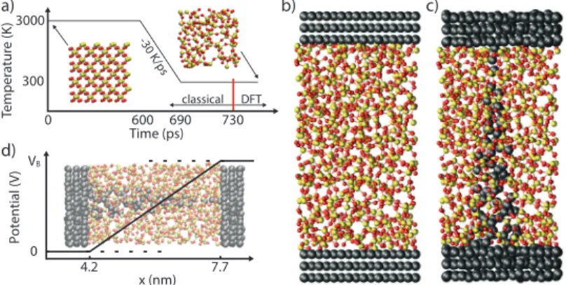
Elaborate schemes are needed to construct suitable amorphous struc- tures and interface them with metallic electrodes. For example, a melt- and-quench approach can be used for that purpose [88]. Starting with a chunk of crystalline oxide or randomly placed atoms, MD must be per- formed for several hundreds of picoseconds at a temperature above the melting point of the oxide. Then, the melt is quenched to 300 K with cool- ing rates in the order of 15 K/ps [87]. Post-quench annealing at room or slightly elevated temperatures can be beneficial to eliminate coordination defects and reduce the stress inside the amorphous structure.
The first atomistic simulation of a complete CBRAM switching cy-
1.2 Conductive Bridging RAM 13 cle was demonstrated by Onofrio et al. [87] using a so-called reactive FF method. In contrast to traditional FFs, reactive force-fields such as ReaxFF [89] are able to describe the formation and breaking of bonds and therefore to model chemical reactions. A much simpler model of a conductive filament can be obtained by manually inserting metal atoms into the amorphous insulating layer instead of explicitly growing a struc- ture [90]. A shape must be defined and all atoms within it are replaced by metal. The result can be used as starting point for reactive MD un- der an electric field. However, models relying on continuous rather than localized electric fields have not lead to realistic filament morphologies so far, at least not for complete ON-OFF switching cycles [91].
The parameterization of force-fields is often tailored such that the processes of interest are accurately described, whereas less relevant phe- nomena are not well accounted for. Therefore, the usage of force-fields to perform MD in complex systems such as CBRAM cells, where many different sub-processes are encountered, can result in misleading behavior.
A higher level of accuracy can be achieved by usingab initio molecular dynamics (AIMD) where the forces acting on each atom are derived from DFT. The latter is a quantum mechanical modeling method that can de- scribe the electronic structure of any given atomic configuration without the need of fitting parameters. However, the high computational demand of AIMD limits the time range it can access to a few picoseconds and the system size to a few thousand atoms [92]. To benefit from the advantages of FFs and DFT, both methods can be combined. First, atomistic filamen- tary type CBRAM structures are created by using FF approaches. Then, the structures are relaxed and optimized using AIMD before a variety of physical properties such as the evolution of the electronic density of states (DOS) [92], the activation energy of ion diffusion [93] as well as the nucleus formation energy [94] in CBRAM cells are extracted with the help of DFT. Due to the disordered nature of the structures, calculating meaningful physical properties can only be achieved by averaging over an ensemble of independent measurements [92].
First principles studies have succeeded in deducing a multitude of characteristics and properties of CBRAM and have thereby enabled the parameterization of high-level modeling techniques. The majority ofab initio modeling works is concerned with evaluating microscopic quanti- ties such as the charge states of metal interstitials in oxide layers, their diffusion barriers and energy of formation, e.g. Ag in SiO2 [95] or Ta2O5 [96], which affects the kinetics of the CBRAM ON-OFF switching as well as data retention. Recent studies have also been concerned with the atomic composition of filamentary structures and their properties [96,97].
Typically, the conductance value of emerging NVM is estimated based on the charge density only. However, only few studies leveraged the power of NEGF in combination with DFT to shed light on the electron transport mechanism in CBRAM [98, 99], VCM [21,100–103], or phase change memory (PCM) [104,105].
1.3 Motivation and Objective of the Thesis
Detailed understanding of electron transport in CBRAM is crucial to improve their implementation, enhance their performance, and ultimately meet the required specifications for mass production. In light of these challenges, gaining insight into the processes taking place within indi- vidual memory cells is vital. The purpose of this thesis is to investigate quantum transport phenomena at the atomic scale in realistically sized, ultra-scaled CBRAM cells. The emphasis is set on the extraction of elec- trical and electro-thermal properties of structures featuring nanoscale filaments as found in the ON-state of such memories. To reach this goal we combined DFT and NEGF, an equally versatile as efficient modeling toolkit. DFT is the most widespread ab initio approach to electronic structure calculations. It is capable of predicting ground-state properties of any material or nanostructure, taking only the initial atomic coor- dinates as input. This is particularly attractive to describe amorphous
1.4 Outline of the Thesis 15 or disordered materials and their interface with metallic electrodes, as encountered in CBRAM. All of which are notoriously difficult to param- eterize. The second component of this framework, NEGF, is a popular statistical approach to out-of-equilibrium quantum transport phenomena.
It can be interfaced with DFT, thereby benefiting from the parameter-free nature of DFT. However, these first principle based calculations are com- putational intensive. Approximate schemes must be devised to address this immense challenge and efficiently evaluate the transport properties of nanostructures with an atomic resolution.
The treatment of CBRAM cells with DFT and NEGF provide in- sight into the properties of nanoscale filaments that cannot be probed experimentally due to their tiny dimensions and their encapsulations within other materials. In modeling, however, the effect of the relocation of individual atoms on electron transport can be traced back and used to elucidate the conductance behavior during the ON-OFF switching process. Moreover, electro-thermal simulations can help identify critical current paths in nanoscale extrusions. The latter can be linked to the reliability of CBRAM cells.
While this work is dedicated to the modeling of CBRAM structures, the developed methodologies can be equally applied to other emerging NVM technologies, as mentioned in the Conclusion chapter.
1.4 Outline of the Thesis
After this introduction about CBRAM cells, their functionality, and their modeling, in Chapter2 the theoretical background of DFT is presented and various atomistic modeling techniques that are employed through- out this thesis are described. Electrical and thermal quantum transport within the NEGF framework is also reviewed and an approximate method to reduce the intensity of quantum transport calculations is outlined.
Chapter3 is dedicated to the mode-space approximation, which is a
numerical procedure to enable quantum transport calculations of large devices at moderate computational cost. The mode-space approximation is then generalized to inhomogeneous simulation domains and applied to CBRAM systems. The scheme is benchmarked against the original real-space description, with a focus on speed and accuracy.
In Chapter4an ultra-scaled Cu/a-SiO2/Cu CBRAM cell is modeled and the results discussed. A technique to implement the dissolution of a filament at the QT level is introduced and the ON-OFF switching of a memory cell is examined with it by extracting the current density at various intermediate stages. The ON-state is further investigated with electro-thermal simulations. Results in the ballistic limit of transport are compared to fully coupled electron and phonon calculations. Finally, the impact of the thickness of the oxide layer on the device stability is revealed.
Chapter 5 focuses on the CE metal, in particular on its influence on the current densities in an Ag filament embedded in SiO2. Multiple metals are used with a fixed filamentary configuration. The characteris- tics of all created structures are extracted and their implications on the computational model requirements are discussed.
Ultimately, conclusions are drawn and an outlook is given in Chap- ter 6. The developed simulation environment is now read to explore alternative material stacks, device geometries, and memory types, e.g.
VCM or breaking junctions.
Chapter 2
Quantum Transport from First Principles
2.1 Introduction
From “first principles” or “ab initio” describes a type of calculation that is directly based on established laws of physics and does not require any empirical inputs nor fitting parameters. When applied to electronic struc- ture investigations, such methods imply that the equations are directly derived from quantum mechanics. This has the obvious advantage no prior knowledge about the properties of the described system is needed, thus precluding any input bias. Furthermore, any kind of system can be treated, whether to reproduce and explain experimental results or to predict a set of properties. The principal challenge posed by ab ini- tioelectronic structure calculations is their heavy computational burden, which limits the size of ensembles that can be studied. Density-functional theory (DFT) [25,26] has become the “de facto” standard in electronic structure calculations for solid-state physics due to the computational efficiency of the method. DFT indeed enables the study of larger systems than other approaches.
Electronic structure calculations are predominantly concerned with determining the ground-state properties of either bulk or isolated sys- tems. Quantum transport (QT) simulations, on the other hand, couple the simulation domain to its environment and enable the treatment of
17
out-of-equilibrium situations. Popular approaches to QT are the Non- equilibrium Green’s Function (NEGF) [27,28] formalism and the quan- tum transmitting boundary method (QTBM) [106]. Both are statistical approaches to solve the Schrödinger equation in the presence of external stimuli that are treated perturbatively. These techniques require a precise description of the electronic structure of the system of interest in the form of a Hamiltonian matrix. A range of methods have been applied to construct this quantity such as the effective mass approximation (EMA) [107], the k·p [108], or the tight-binding method (TB) [109]. Their re- striction to a single point in the Brillouin Zone and/or their reliance on empirical parameterizations limits their predictive capabilities and restricts their use to materials with known properties. A more flexible approach to QT is achieved by combining it withab initio electronic structure calculations [30].
The theory behind these simulations is presented in this chapter as follows: first the electronic structure procedure behind density-functional theory is summarized. Subsequently, the NEGF formalism is outlined and its connection to DFT described. Lastly, the mode-space (MS) ap- proximation for use together with NEGF, is introduced. It can help tackle the computational burden induced by combining NEGF and DFT.
2.2 Density-functional Theory
The properties of a stationary quantum mechanical system can be entirely determined by its many-body wave functionΨ. The latter obeys the time- independent Schrödinger equation
HˆΨ =EΨ, (2.1)
which is the fundamental quantum mechanical problem that needs to be solved. Here,E is the total energy of the system and the corresponding
2.2 Density-functional Theory 19 Hamiltonian operatorHˆ can be separated into a nuclear and electronic kinetic energy term Tˆc andTˆe, a nuclear-nuclear and electron-electron interaction term Uˆc and Uˆn, and lastly a nuclear-electron interaction term Uˆce. In an atomic structure with Nc cores andNe electrons, the many-bodyHˆ is given by
Hˆ =−
Nc
X
n=1
~2 2mn∇2−
Ne
X
i=1
~2 2m0∇2+ 1
4π0 X
n<m
ZnZme2
|Rn−Rm| + 1 4π0
X
i<j
e2
|ri−rj|− 1
4π0
X
n,i
Zne2
|Rn−ri|,
(2.2)
where mn andm0are the masses of the cores and the rest mass of elec- trons, respectively, Zn is the number of protons in atom n,Rn and ri are the positions of atomnand electroni, respectively,~,e, and0 are the reduced Planck’s constant, the electron charge, and the permittivity of free space. With this Hamiltonian the wave function Ψ becomes a function that depends on3(Nc+Ne)variables, thus resulting in a prob- lem that can only be solved analytically for the simplest systems such as harmonic oscillators or the hydrogen atom. For realistic applications Eq. (2.1) has to be solved numerically.
Even numerically, Eqs. (2.1)-(2.2) remain extremely challenging to handle without further approximations. The most fundamental one is the Born-Oppenheimer approximation, which separates the motion of the atomic nuclei and of the electrons. The difference in masses justifies the assumption that the particles, the core and the electrons, move on different time scales, which implies that the electrons can always relax to their ground state within the time scale the atomic cores need to move.
This effectively decouples the wave function of the core and electrons and allows one to describe the total wave function Ψas the product of the
two separate components, the nucleiΨcand electronΨe. In this picture the electrons move freely within the external potential induced by the nuclei. The Hamiltonian for the electrons is then given by
Hˆe= ˆTe+ ˆUe+ ˆV , (2.3) whereTˆe and Uˆekeep their definition from Eq. (2.2), whereas the last termVˆ describes the external potential induced by the nuclei. Owing to their large mass, the atomic cores are typically treated in a classical man- ner, as explained in Section2.2.1. This restricts the quantum mechanical part to the description of the electrons, thereby significantly reducing the computational complexity. Nevertheless,Ψestill is a function of3Ne spatial variables.
Multiple methodologies to approximate Eq. (2.3) have been developed with a wide range of computational requirements and accuracy. The gold standard in computational chemistry is set by the coupled-cluster (CC) technique [110], which uses the exponential cluster operator to express the electron correlation. By approximating the exponential with a power series CC offers a systematic approach to converge the wave function.
Typically, CCSD(T) which includes first- and second-order terms and treats the third-order term perturbatively, delivers results which agree ex- ceptionally well with experiments [110]. CC, however, scales with(O6)to (O8)with respect to the number of electrons, depending on the number of terms included. This fact renders CC impractical for systems beyond a few dozen atoms. Post-Hartree-Fock methods introduce further approx- imations and reduce the polynomial scaling down to(O5), though it still limits them to fairly small atomic configurations or molecules. The high polynomial scaling can be avoided altogether by reformulating Eq. (2.1), such thatΨedoes not have to be calculated. A powerful approach to this endeavor is given by the Hohenberg-Kohn (H-K) theorems, which lay out the foundation of DFT. The latter relies on the electron density ρ(r), which is a function of only three spatial variables. For this reason, DFT
2.2 Density-functional Theory 21 is the most widely used method for electronic structure calculations.
The first H-K theorem states that two systems of electrons, which have the same ground-state densityρ(r), necessarily reside in the same external potentialV(r), up to a constant. That is, the external potential and the total energy are unique functionals of the ground-state density.
Not only is the electron density determined by the wave function ρ(r) =
Z dr23...
Z
dr3NeΨ∗e(r, r2, ..., rNe)Ψe(r, r2, ..., rNe), (2.4) but the reverse is true as well
Ψ0(r1, ..., rNe) = Ψe[ρ0(r)] (2.5) for the ground-state wave function. Consequently,ρ0(r)determines all observable properties of a system of electrons and it is not necessary to compute the true many-body wave function. This is particularly attrac- tive becauseρ(r) only depends on the 3 spatial coordinatesr =x, y, z instead of3Ne variables, r1, ..., rNe, which greatly reduces the compu- tational impact. The second H-K theorem states that the functional F[ρ(r)], which delivers the ground-state energy E, returns the lowest possible energy if and only if the electron density is the true ground-state density. This implies that a functional exists such that
E[ρ(r)] =F[ρ(r)] + Z
dr3V(r)ρ(r) (2.6) whereE[ρ(r)]reaches its minimum at the true ground stateρ0(r). There- fore, a variational principle can be deduced to compute the ground-state densityρ0(r)of any system where the only input isV(r), which in turn is solely determined by the presence and position of the atomic nuclei.
While the H-K theorems prove that the many-body wave function does not need to be computed, they do not provide the functionalF[ρ(r)]to obtainE[ρ(r)]. The many-body interactions do not disappear, but they
are merely hidden in the functional.
Instead of attempting to solve the many-body Schrödinger equation di- rectly, Kohn and Sham introduced an auxiliary system of non-interacting particles [26]. Each of them obeys the single-particle Schrödinger equation
[− ~2
2m +Vs(r)]ψi(r) =Eiψi(r). (2.7) While the wave functionsψi(r)solving Eq. (2.7) have no physical mean- ing themselves, they give the correct ground-state density though
ρ0(r) =
N
X
i=1
ψi∗(r)ψi(r). (2.8)
The non-interacting particles reside in the single-electron effective po- tentialVs(r), which contains the external potentialV(r)as well as the electron-electron interactions:
Vs(r) =
Z e2ρ(r0)
|r−r0|d3r0+Vxc[ρ(r)] +V(r). (2.9) The first term of Eq. (2.9) is called Hartree potential and contains the Coulomb repulsion between the electrons in a mean-field approach. The computationally challenging many-body interactions are cast into the sec- ond term called exchange-correlation potentialVxc (xc-functional). To date the exact form of this functional has not been universally determined, but a multitude of approximations exist and the search for improved forms is still ongoing [111,112]. The two H-K theorems together with the Kohn- Sham equations define the KS-DFT scheme, subsequently referred to as DFT. It should be noted that KS-DFT is not the only approach, but by far the most widespread one [113]. Furthermore, the theory behind DFT is exact. The inaccuracies of modern implementations of DFT originate from the approximations made to render the equations computation- ally tractable, predominantly those applied to Vxc, sometimes termed
2.2 Density-functional Theory 23 density-functional approximation (DFA). Since the entire computational procedure is solely derived from theory and does not require empirical inputs, DFT is a first principle orab initiomethod. For historical reasons the second denomination (ab initio) is often reserved to wave function based methods. The two terms are used interchangeably in this work.
Numerous forms of xc-functionals have been proposed. They are typi- cally categorized according to the level of approximation in the so-called Jacob’s ladder [114]. On the lowest rung of the ladder one finds local- density approximation (LDA) functionals. These are derived from the homogeneous electron gas model and assume the charge density to be lo- cally constant to model the exchange and Coulomb correlations. Despite its crude level of approximation, the LDA functional is rather successful at describing many properties of metallic compounds. Its success can be attributed to the fact that errors in the exchange and correlation energies tend to cancel out. For semiconductors or insulators as well as molecular systems the accuracy of LDA greatly varies. The second rung of Jacob’s ladder is made of the large family of generalized-gradient approximation (GGA) functionals. In addition to the magnitude of the local density GGA also includes its gradient to estimate the correlation effects. Among the GGA-implementations the formulation of Perdew- Burke-Ernzerhof (PBE) [115] is consistently the most popular. While not the most accurate functional it produces reasonable results for most systems. Among the shortcomings of LDA and GGA, the most significant one forab initioQT is that the band gap of semiconductors and insula- tors is severely underestimated. Meta-GGA functionals implement the next level of theory over GGA by adding a kinetic term to the functional, related to the second derivative of the density [116]. Hybrid functionals constitute the fourth rung of Jacob’s ladder. They mark a huge step upwards, both in terms of accuracy as well as computational complex- ity. Most hybrid functionals rely on GGA where the exchange term is improved by adding a fraction of the exact Hartree-Fock (HF) exchange [117]. Many properties such as the band gap and binding energies are
much more accurately predicted by hybrid functionals as compared to GGA or LDA. This enhancement comes at the prize of worse polynomial scaling and far larger memory requirements, rendering the use of hybrid functionals impractical for systems containing many atoms. In addition to mixing HF and GGA exchanges into the functional, second-order per- turbative Coulomb correlation can be introduced [118]. These double hybrid functionals can provide high accuracy at the cost of even higher computation cost. Because of this they are restricted to niche application, but are slowly gaining in popularity.
Independent of Jacob’s ladder, functionals can also be grouped by their composition. One such group is purely or mostly derived from theory with zero or few fitting parameters such as the PBE functional. The latter is often chosen to minimize the error of various properties over a large range of different compounds or molecules. The second group consists of functionals that are based on a number of parameters, which are fitted to accurately reproduce specific properties of certain materials such as B3LYP [119], which is tailored for organic molecules. Both forms have their respective advantages: fitted functionals are often more accurate when correctly employed, i.e. on compounds that are similar to the ones for which the xc-functional was parameterized. PBE-type functionals, on the other hand, are typically less accurate than the fitted ones, but have the advantage of being applicable to a wide range of compounds, i.e. they are more versatile [120].
2.2.1 Molecular Dynamics
Molecular dynamics (MD) is a simulation approach to investigate the movements of atoms and probe the dynamic evolution of an ensemble.
The considered particles are allowed to interact for a certain period of time by numerically integrating Newton’s equations of motion. MD can be combined with DFT as a consequence of the Born-Oppenheimer approximation, which separates the treatment of electrons and nuclei.
2.2 Density-functional Theory 25 During the electronic structure calculation, the atoms are frozen in place and are only accounted for through the external potential in Eq. (2.3).
Once the ground-state electron density is obtained, the forces acting on the atoms can be derived as the negative gradient of the potential energy with respect to the atom positions. Because the potential energy surface is obtained from first principles this type of simulation is calledab initio molecular dynamics (AIMD) or alternatively Born-Oppenheimer molecular dynamics (BOMD).
Different ensembles can be defined within MD. The simplest form is the microcanonical ensemble (NVE), where the number of particles (N), the volume (V), and the total energy (E) of the system are conserved. The particles can freely exchange potential for kinetic energy and vice-versa.
The instantaneous temperature T of the ensemble is defined by equating the kinetic energy of the atoms to 3/2kBT, where kB is Boltzmann’s constant. The estimated temperature can change over time when the system is undergoing exo- or endothermic reactions. Alternatively, a canonical ensemble (NVT) can be defined, where the temperature instead of the total energy is conserved. A thermostat couples the finite simulation domain to a bath which absorbs (injects) kinetic energy from (into) the system, thereby regulating the instantaneous temperature. Additionally, the pressure tensor can be derived from the electron density. By applying a barostat to the AIMD simulation, the pressure (P) within the ensemble can be controlled and kept constant. Deploying both a thermostat and a barostat to an AIMD simulation results in an isothermal-isobaric (NPT) ensemble.
The time step employed to integrate the equations of motions should be kept small enough to capture all atomic movements The shortest time scale to consider typically is the phonon oscillation period. Therefore, time steps in the order of femtoseconds are required. Because of the large computational burden induced by DFT and the short time steps required to capture all relevant motions, AIMD simulations are typically restricted to dozens of picoseconds and several 100’s to few 1000’s of atoms.
As an alternative, instead of integrating the forces over time, the atom positions can be optimized such that the force on each atom vanishes. This process of driving the ensemble towards a local minimum in the potential energy surface is referred to asgeometry optimization throughout this thesis. By including the pressure tensor in the optimization process, the lattice parameter of the unit cell under consideration can be optimized as well. Together with the optimization of the forces this process is termed cell optimization.
2.3 Quantum Transport
1The NEGF formalism offers a powerful framework to calculate the non- equilibrium properties of quantum mechanical systems [121]. It is widely used to perform quantum transport (QT) simulations [122, 123]. This approach to non-equilibrium statistical mechanics is based on the works of Kadanoff and Baym [27] and Keldysh [28]. It requires a description of the electronic structure of the system under study in the form of a Hamiltonian matrix. Approaches relying on first principles concepts, where the Hamiltonian matrix is obtained from DFT calculations, are known asab initioQT [30,124,125]. The coupling of NEGF and DFT was introduced by Lang [124], where the representation of the device was based on DFT and the electrodes modeled using a jellium approximation.
Fully atomistic simulations were proposed by Taylor et al. [30] featuring an atomistic representation based on DFT for both the device region and the contacts. Since these pioneering works, several packages capable of treating quantum transport from first principles have been developed [126–131]. Some of them are freely, others commercially available.
The majority of DFT+NEGF calculations are performed in the bal- listic limit of transport, where the energy of each particle is conserved throughout the simulation domain. The effect of inelastic interactions
1 This section is based on [50]
2.3 Quantum Transport 27 can naturally be incorporated in NEGF through the use of scattering self-energies [132]. Besides pure electrical or thermal transport, coupled electro-thermal simulations can be perturbatively carried out through the self-consistent Born-approximation (SCBA) [31,133]. Owing to the large computational burden induced by the SCBA, such simulations are typi- cally restricted to small systems or require large computational resources.
Furthermore, calculating the phonon properties and the electron-phonon coupling from first principles is a challenging task [134,135]. Nevertheless, such calculations have been applied to a wide range of nanoscale devices going from 2-D field-effect transistors (FETs) [134], FinFETs [135], or CBRAM cells [136] to the modeling of inelastic electron-tunneling spec- troscopy (IETS) in molecular junctions [137,138].
It should be emphasized that the SCBA is not the only possibility to account for electro-thermal effects. Lowest order-expansion techniques have been used as well. They have a lower computational burden, but at the cost of additional approximations [137,139]. Due to its pertur- bative nature, SCBA may fail to converge in the presence of strong electron-phonon coupling or other scattering mechanisms representing strong interactions. An exact but also computationally more expensive techniques capable of treating such systems is the hierarchical equations of motion [140].
This section is dedicated to the description of electro-thermal QT calculations with a focus on DFT-based electronic structure representa- tions within the SCBA. The following subsections describe the coupling of DFT with NEGF for the case of electrical and thermal transport.
Lastly, the coupling of electrons and phonons via scattering self-energies is explained.
2.3.1 Electron Transport
As described in the previous section, DFT is a powerful method to calcu- late the electronic structure of atomic systems. Thus, the most advanced