physica status solidi
Facile preparation of Au(111)/MICA substrates for high-quality graphene nanoribbon synthesis
M. G. Hell
*,1, B. V. Senkovskiy
1, A. V. Fedorov
1, A. Nefedov
2, C. W ¨ oll
2, A. Gr ¨ uneis
11
II. Physikalisches Institut, Universit¨at zu K¨oln
2
Institut f¨ur Funktionelle Grenzfl¨achen, Karlsruher Institut f¨ur Technologie, Eggenstein-Leopoldshafen
Received XXXX, revised XXXX, accepted XXXX Published online XXXX
Key words: Graphene nanoribbon, DBBA, Au(111), XPS, NEXAFS, Raman
∗
Corresponding author: e-mail hell@ph2.uni-koeln.de , Phone: +49 - 221 - 470 7078
A setup for the preparation of oriented Au(111)/mica thin films of ∼100 nm thickness as an active substrate for graphene nanoribbon growth is shown. Low-energy electron diffraction shows that the Au(111) thin films have a single crystallographic orientation over the whole surface area. Graphene nanoribbons are synthesized by the bottom-up approach via surface polymerization of precursor molecules that are evaporated onto the cat- alytically active Au(111)/mica substrate. The graphene nanoribbons are investigated by a combination of res- onance Raman, X-ray photoemission spectroscopy and near-edge X-ray
absorption fine structure spectroscopy confirming a nanoribbon quality equal to nanoribbons grown on com- mercially available single-crystal Au(111) substrates.
The present work therefore establishes the in-situ prepa- ration of Au(111)/MICA as an inexpensive and simple method to prepare substrates of desired shape and thick- ness for surface polymerization reactions which are of interest to a growing community of researchers working on graphene nanoribbons.
Copyright line will be provided by the publisher
1 Introduction Carbon nanomaterials have been in the focus of condensed matter physics for a long time already. Following fullerenes, nanotubes and graphene the latest member of this materials’ family are graphene nanoribbons which are receiving lots of attention [1–4].
Ultranarrow graphene nanoribbons (GNRs) are ∼1 nm wide stripes of graphene with defined edges (zig-zag or armchair). They can be produced in high-quality by bottom-up nanotechnology [2]. A large variety in struc- tures can be engineered by simply varying the precursor molecule. Probably the best studied is the surface polymer- ization of 10,10-dibromo-9,9-bianthryl (DBBA) molecules which yields armchair graphene nanoribbons with a width of 7 atoms (7-AGNRs) [2, 5]. Modifications of the pre- cursor molecule has successfully allowed for the bottom up synthesis of boron [6, 7] and sulphur doped nanorib- bons [8]. Moreover, varying the width of the precursor
molecules changes the nanoribbon width and hence al- lows for band-gap engineering. For any of the precursors, surface polymerization can be obtained on atomically flat Au(111), Ag(111) or Cu(111) surfaces [2, 9, 10] (or their vicinal cuts such as Au(788) [11]). Single crystals have been used extensively for nanoribbon synthesis however their high cost is prohibitive for high-yield and scalable growth on an industrial scale. Nevertheless an atomically flat metal surface is needed to achieve reproducible and high-quality nanoribbon synthesis. The present manuscript addresses these needs. Here we show that the application of a well-known recipe for growth of Au(111) on mus- covite mica [12] provides surfaces that can be synthesized in-situ and are inexpensive and easy-to-prepare.
2 Synthesis The Au(111)/MICA synthesis was per- formed in a small growth chamber under high vacuum
Copyright line will be provided by the publisher
2 M. Hell et al.: Facile preparation of Au(111)/MICA substrates for high-quality graphene nanoribbon synthesis
conditions with the base pressure p < 10
−6mbar. Af- ter Au(111) growth these substrates have been transferred in air into an ultra-high-vacuum (UHV) preparation cham- ber where the in-situ GNR synthesis and spectroscopy was performed. Prior to the GNR growth the Au(111) surfaces where gently annealed at 200
◦C to remove contaminants from the air exposure.
In figure 1(a) we show the core of the setup for prepa- ration of Au(111)/MICA. It is a homebuilt sample manipu- lator which consists of a sample pocket, thermocouple and a water cooled quartz microbalance. Figure 1(b) depicts a sketch of how the sample plate (an Omicron type plate made out of Mo) can be inserted into the sample pocket.
To prepare an Au(111) film we first mount a freshly ex- situ cleaved mica on the sample plate using Ta stripes, place into the sample pocket and evacuate it to a pressure lower than 10
−6mbar. We then clean and degas the sample by annealing to 300
◦C for at least 12 hours. Hereafter the mica is annealed to 500
◦C for ∼1 min in order to remove contaminants. To obtain thick Au layer, the evaporator was placed close (about 5 cm) in front of the sample manip- ulator. The Au atom flux is calibrated conveniently just before deposition by a quartz microbalance and mounted above the sample pocket [see Figure 1(a)]. It is known [12]
that for crystalline Au growth the mica must be kept at 300
◦C during deposition. We found that the Au deposi- tion rate must be at least 0.5 ˚ As
−1in order to obtain low energy electron diffraction (LEED) spots. After Au depo- sition the sample is annealed for 12 h at 300
◦C. Figure 1(c) depicts a photograph of an Au/mica film. Atomic force mi- croscopy (AFM) enables precise thickness measurements and we have used AFM in order to calibrate the quartz mi- crobalance tooling factor.
Figure 1(d) shows an atomic force microscopy (AFM) scan across the edge of the Au film. The edge was defined by the Ta stripe and therefore not perfectly sharp as some Au can grow underneath the stripe close to its edge. AFM allows to measure the thickness of the Au film which is defined by the height difference of the region under the Ta stripe to the maximum. An Au film prepared in such a way does not show a sharp pattern in low-energy elec- tron diffraction (LEED). Hence such films are not ordered.
In order to obtain a sharp LEED, a second annealing step at a temperature of 600
◦C is needed. This will cause the structuring of the Au(111) sample. The duration of the last annealing step is depending on the thickness of the sam- ple. For a regular sample of 50-100 nm a duration of 30 minutes is sufficient. Hereafter we were able to identify a sharp LEED pattern with a sixfold rotational symmetry which we ascribe to the Au(111) surface structure. Two typical LEED patterns for electron energies of 50 and 70 eV taken prior to molecular deposition are shown in Fig- ure 1(e), correspondingly. By scanning the sample across the LEED spot, we could verify that the LEED pattern does not change. This indicates that all domains have the same orientation in the topmost atom layers.
The synthesis of GNRs was performed by evapora- tion of DBBA molecules onto a freshly prepared Au(111) surface, followed by annealing steps. The DBBA was evap- orated from a quartz crucible using a homebuilt organics evaporator with a thermocouple attached to the molecule reservoir. The deposition rate was controlled using a quartz microbalance. About 10 ˚ A of precursor molecules (using the graphite density and Z-factor) were evaporated onto the Au surface which was kept at room-temperature. Ef- fectively only a part of the DBBA will form ribbons and the remainder will simply sublimate. This is due to a weaker bonding between molecules to each other with respect to the molecule-substrate bond. In order to carry out DBBA debromization and cyclodehydrogenation reactions, the temperatures must be known quite precisely (to an accu- racy better than 5
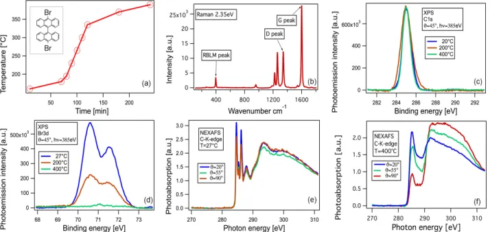
◦C) and annealing has to be carried out slowly. We have therefore calibrated this curve not with the thermocouple shown in Figure 2(a), instead we have spot- welded a thermocouple onto an empty sample holder and recorded the temperature directly where usually the mica is located. Figure 2(a) shows the curve of temperature ver- sus time we have used to synthesize graphene nanoribbons from a 10 ˚ A thick DBBA film/Au(111)/mica. The inset to Figure 2(a) depicts a sketch of the DBBA molecule.
3 Results The straightforward way to proof the formation of GNRs is resonance Raman spectroscopy.
GNRs have a radial-breathing like mode at low energies (397cm
−1) for 7-AGNR [13]) which is their fingerprint.
Due to the high resonance enhancement that occurs if the laser energy used matches the separation of van-Hove- singularities in the density of electronic states, very strong Raman spectra from submonolayer coverages of ribbons can be obtained easily. The E
22resonance transition for 7-AGNRs can be excited by a 2.35 eV laser [14]. Figure 2(b) depicts the Raman spectra obtained. It can be seen that all GNR related modes appear. In particular, the de- fect induced D band is even lower than of most GNRs synthesized on single crystal substrates. [2]
Then we turn to the x-ray photoemission spectroscopy (XPS) measurements on C and Br core levels which have been carried out at the HESGM beamline of the BESSY II synchrotron (Helmholtz-Zentrum Berlin, Germany). Fig- ures 2(c) and 2(d) depict the C1s and Br3d core levels dur- ing three annealing steps (room temperature, 200
◦C and 400
◦C). The photon energy used was set to hν=385eV. It can be seen that the intensity for C1s is not changing dur- ing polymerization and a lot of the Br3d intensity vanishes after the first annealing step of 200
◦C. Further annealing to 400
◦C causes all Br3d intensity to disappear, indicating that the Br has left the Au surface and that all the molecules are now either in their radical form with dangling C atoms or already polymerized.
After that near edge x-ray absorption fine structure (NEXAFS) spectroscopy have been performed in partial yield mode. Figure 2(e) depicts the C K-edge NEXAFS
Copyright line will be provided by the publisher
pss header will be provided by the publisher 3
Figure 1 (a) Homebuilt sample manipulator with empty sample pocket, filament and high voltage for e-beam heating, thermocouple and water cooled quartz microbalance (b) schematics of a sample inserted into the sample pocket (c) MICA after deposition of Au (d) AFM measurement of Au(111) height on MICA across the location of the Ta stripe (e) LEED diffraction pattern of Au(111)/mica at 50 eV and at 70 eV.
Figure 2 (a) Temperature programmed GNR synthesis performed with a programmable power supply (b) Raman spectrum of 7-AGNRs on Au(111) measured with a 2.35 eV laser (c,d) XPS spectra of C1s and Br3d core levels (e,f) NEXAFS spectra of deposited DBBA molecules immediately after deposition and after annealing to 400
◦C.
spectra measured at three different incidence angles on DBBA molecules deposited on Au before annealing. The sharp features at the photon energy range 284-290 eV are related to transitions from the C1s core levels to the un-
occupied π
∗molecular orbitals. Since a significant angle dependence is absent we can conclude that the precur- sor molecules are disordered or partially twisted with a small tendency to planar orientation. After annealing up
Copyright line will be provided by the publisher
4 M. Hell et al.: Facile preparation of Au(111)/MICA substrates for high-quality graphene nanoribbon synthesis
to 400
◦C a drastic change in the electronic structure takes place. The corresponding NEXAFS spectra are shown in Figure 2(f). Firstly, the sharp peaks in the π
∗resonance at 285 eV disappear and a rather broad peak appears. Sec- ondly, the angle dependence of this new peak as well as of σ
∗resonances now much stronger. In particular the π
∗related peak around 285 eV has a minimum and σ
∗related peaks at the photon energy range 290-310 eV have a max- imum for normal incidence (90
◦, the electric field vector is parallel to the ribbon plane). This angle dependence in- dicates that the GNRs are lying planar on the surface after cyclodehydrogenation.
4 Conclusions In summary we have shown an inex- pensive and simple method to prepare high quality dispos- able Au(111)/MICA substrates for the surface polymeriza- tion of graphene nanoribbons using a molecular precusor.
The spectroscopic investigation of GNR samples grown on this substrate indicates that the GNRs have spectra identi- cal to those obtained from single crystal substrates. This has been checked using Raman spectroscopy, XPS and NEXAFS. The Au(111)/mica substrates are mich cheaper than the single crystals, and, thus, can be used for experi- ments, that are harmful for substrates (e.g. chemical treat- ment and functionalization or transferring the GNRs on to the insulators/semiconductors). The method introduced here is important for the growing GNRs community which wishes to synthesize GNRs on purpose made substrates.
Acknowledgements M.H., B.S. and A.G. acknowledge the ERC grant no. 648589 ’SUPER-2D’, funding from Quantum Matter and Materials and DFG project GR 3708/2 − 1. A.N. and C.W. acknowledge funding from the Science and Technology of Nanosystems program. Research supported by the U.S. Depart- ment of Energy (DOE), Office of Science, Basic Energy Sciences (BES), under Award no. DE − SC0010409 (design, synthesis and characterization of molecular building blocks) and the Cen- ter for Energy Efficient Electronics Science NSF Award 0939514 (SPM imaging and spectroscopy). We also thank Helmholtz Zen- trum Berlin for the beamtime allocation.
References
[1] L. Grill, M. Dyer, L. Lafferentz, M. Persson, M. V. Peters, and S. Hecht, Nature Nanotechnology 2, 687–691 (2007).
[2] J. Cai, P. Ruffieux, R. Jaafar, M. Bieri, T. Braun, S. Blankenburg, M. Muoth, A. P. Seitsonen, M. Saleh, X. Feng, K. Mullen, and R. Fasel, Nature 466(7305), 470–
473 (2010).
[3] Z. Chen, Y. M. Lin, M. J. Rooks, and P. Avouris, Physica E:
Low-dimensional Systems and Nanostructures 40(2), 228 – 232 (2007), International Symposium on Nanometer- Scale Quantum Physics.
[4] P. Ruffieux, J. Cai, N. C. Plumb, L. Patthey, D. Prezzi, A. Ferretti, E. Molinari, X. Feng, K. M¨ullen, C. A.
Pignedoli, and R. Fasel, ACS Nano 6(8), 6930–6935 (2012).
[5] A. Narita, X. Feng, and K. M¨ullen, The Chemical Record 15(1), 295–309 (2014).
[6] S. Kawai, S. Saito, S. Osumi, S. Yamaguchi, A. S. Foster, P. Spijker, and E. Meyer, Nat Commun 6, 8098 (2015).
[7] R. R. Cloke, T. Marangoni, G. D. Nguyen, T. Joshi, D. J.
Rizzo, C. Bronner, T. Cao, S. G. Louie, M. F. Crommie, and F. R. Fischer, Journal of the American Chemical Soci- ety 137(28), 8872–8875 (2015), PMID: 26153349.
[8] G. D. Nguyen, F. M. Toma, T. Cao, Z. Pedramrazi, C. Chen, D. J. Rizzo, T. Joshi, C. Bronner, Y. C. Chen, M. Favaro, S. G. Louie, F. R. Fischer, and M. F. Crommie, The Journal of Physical Chemistry C 120(5), 2684–2687 (2016).
[9] K. A. Simonov, N. A. Vinogradov, A. S. Vinogradov, A. V.
Generalov, E. M. Zagrebina, N. M˚artensson, A. A. Cafolla, T. Carpy, J. P. Cunniffe, and A. B. Preobrajenski, Growth and structure of graphene nanoribbons on substrates with different reactivity, www.maxlab.se.
[10] K. A. Simonov, N. A. Vinogradov, A. S. Vinogradov, A. V. Generalov, E. M. Zagrebina, G. I. Svirskiy, A. A.
Cafolla, T. Carpy, J. P. Cunniffe, T. Taketsugu, A. Lyalin, N. M˚artensson, and A. B. Preobrajenski, ACS Nano 9(9), 8997–9011 (2015).
[11] S. Linden, D. Zhong, A. Timmer, N. Aghdassi, J. H.
Franke, H. Zhang, X. Feng, K. M¨ullen, H. Fuchs, L. Chi, and H. Zacharias, Phys. Rev. Lett. 108(21) (2012).
[12] R. Colton, W. Ebeling, J. Frommer, H. Gaub, A. Gewirth, R. Guckenberger, and J. Rabe, Wiley; 1 edition ISBN-13:
978-0471959120 (August 7, 1998).
[13] L. Talirz, P. Ruffieux, and R. Fasel, Adv. Mater.(feb), n/a–
n/a (2016).
[14] F. Krakau, Bachelor thesis, University of Cologne (2014).
Copyright line will be provided by the publisher