• Keine Ergebnisse gefunden

Combined STM/AFM with functionalized tips applied to individual molecules

N/A
N/A
Protected

Academic year: 2021

Aktie "Combined STM/AFM with functionalized tips applied to individual molecules"

Copied!
170
0
0

Wird geladen.... (Jetzt Volltext ansehen)

Volltext

(1)

Combined STM/AFM with functionalized tips applied to

individual molecules

Chemical reactions, geometric structure and charge distribution

Dissertation zur Erlangung des Doktorgrades der Naturwissenschaften (Dr. rer. nat.)

der Fakultät für Physik der Universität Regensburg

vorgelegt von Florian Albrecht

aus Passau

2016

(2)

1

Die Arbeit wurde von Prof. Dr. Jascha Repp angeleitet.

Das Promotionsgesuch wurde am 5. Juli 2016 eingereicht.

Das Promotionskolloquium fand am 27. Oktober 2016 statt.

Prüfungsausschuss: Vorsitzender: PD Dr. Falk Bruckmann

1. Gutachter: Prof. Dr. Jascha Repp

2. Gutachter: Prof. Dr. Josef Zweck

weiterer Prüfer: Prof. Dr. Christoph Strunk

(3)

Abstract

Scanning probe microscopy (SPM) methods allow for investigations of the atomistic world in real space. While scanning tunneling mi- croscopy (STM) is sensitive to the electronic structure of the sample, its geometry can be explored by means of atomic force microscopy (AFM). Suitable functionalization of the AFM tip enables resolving the chemical structure of individual molecules at low temperatures in ultrahigh vacuum. Combining STM and AFM detection schemes in one setup facilitates simultaneous examination of the electronic and the geometric structure of single (molecular) adsorbates.

This work employs SPM with functionalized tips on individual mole- cules in three topics:

The capability of structure determination is widened to non-planar and strongly deformed molecules. The required information is deduced from either full three-dimensional data sets or from images along the adsorbed molecule’s symmetry planes that are perpendicular to the sample surface.

On-surface chemical reactions are studied in great detail. For two exemplary cases, we investigate the reaction pathway of a thermally activated planarization reaction, and we examine the interplay of elec- tronic and geometric structure in the tip-induced formation of a metal- organic complex.

Finally, we use AFM to image the charge distribution in individual

metal-organic molecules with polar bonds. Introducing a novel spec-

troscopy technique we resolve charge contrast along individual polar

bonds.

(4)
(5)

Contents

Abstract iii

1 Introduction 1

2 Theory background 3

2.1 Scanning Tunneling Microscopy . . . . 3

2.1.1 STM imaging . . . . 5

2.1.2 Scanning Tunneling Spectroscopy . . . . 5

2.2 Atomic Force Microscopy . . . . 6

2.2.1 Static AFM . . . . 6

2.2.2 Dynamic AFM . . . . 8

2.3 Kelvin probe force methods . . . . 13

3 Experimental setup and methods 25 3.1 LT-UHV combined STM/AFM apparatus . . . . 25

3.2 qPlus sensor . . . . 26

3.3 Sample preparation . . . . 31

3.4 Modes of data acquisition . . . . 31

3.5 Tip functionalization . . . . 34

3.6 Tip height conventions . . . . 36

4 Preliminary experiments on tip functionalization 37 4.1 Characterization of CO functionalized tip . . . . 37

4.2 Contrast evolution on molecules with CO tip . . . . . 39

4.3 Tip-change induced artifacts in KPFS results . . . . . 41

(6)

Contents

5 Characterization of a surface reaction by means of AFM 45 5.1 AFM in on-surface chemistry . . . . 45 5.2 Methods . . . . 46 5.3 Structure identification of the reactant . . . . 47 5.4 Molecular species after thermally activated on-surface

reaction . . . . 51 5.5 Discussion of the reaction pathway . . . . 54 5.6 Conclusion . . . . 56 6 Determining conformational details of strongly deformed

molecules 57

6.1 Tetraphenylporphyrin molecules in surface science . . 58 6.2 Details of the setup . . . . 59 6.3 Conventional imaging . . . . 59 6.4 A new method: Vertical imaging . . . . 63 6.5 Reversible conformational switching of Cu-TPP . . . . 66 6.6 Conformational conversion of 2H-TPP . . . . 70 6.7 Conclusion . . . . 72 7 Interplay of electronic and geometric structure upon

an on-surface reaction 73

7.1 SPM in single molecular chemistry . . . . 73 7.2 Experimental and simulation methods . . . . 74 7.3 Complex formation and geometric structure . . . . 75 7.4 Electronic structure of a monomer and a complex . . . 78 7.5 Electronic coupling model . . . . 81 7.6 Conclusion . . . . 86 8 Visualizing the polarity of an individual chemical bond 89 8.1 Charge sensing in AFM . . . . 89 8.2 Methods . . . . 90 8.3 Intramolecular charge distribution deduced from KPFS

maps . . . . 92

8.4 Concept of deducing dipoles from ∆f(z) spectroscopy 97

(7)

Contents

8.5 Simplifications and assumptions made for the determi-

nation of dipoles . . . . 100

8.6 Results of the new dipole detection method . . . . 102

8.7 Conclusion . . . . 105

9 Local tunneling decay length and KPFS 107 9.1 STM-based charge determination . . . . 107

9.2 Experimental methods . . . . 109

9.3 Effect of sample topography on decay length . . . . . 111

9.4 Choice of Systems . . . . 112

9.5 Experimental results of κ mapping and KPFS . . . . . 113

9.6 Quantitative failure of κ mapping . . . . 117

9.7 Conclusion . . . . 119

10 Summary and Outlook 121 A Additional data for the investigation of bond polarity 125 A.1 Assignment of side groups in ClAnCN . . . . 125

A.2 Details of fitting procedure . . . . 125

A.3 Full set of dipole maps deduced using different interac- tion potentials . . . . 127

A.4 DFT-calculated charge distribution of F 12 C 18 Hg 3 and H 12 C 18 Hg 3 . . . . 129

Bibliography 131

List of Abbreviations and Symbols 153

Contributors to this work 155

Acknowledgments 157

List of Publications 159

(8)
(9)

1 Introduction

The invention of the scanning tunneling microscope (STM) by G.

Binnig and coworkers paved the way for imaging individual atoms in real space [1]. The capability of STM to move single adsorbates on the sample surface allows for the controlled build-up of atomic structures [2]. Scanning tunneling spectroscopy (STS) enables the de- tection of the electronic structure of the sample [3]. Using ultra-thin insulators as decoupling layer facilitates probing the unperturbed elec- tronic structure and orbital shape of individual adsorbates [4]. Hence, STM enables experiments and sample design on the single atom level but is limited in two ways: On the one hand, it requires a conducting sample. On the other hand, it probes the electronic structure that, in general, must not be interpreted in terms of the sample’s geometry only.

To get access to the geometry on the atomic scale, G. Binnig et al.

introduced the atomic force microscope (AFM) [5]. The final step to directly resolve the chemical structure of single molecular adsorbates was introduced by L. Gross and coworkers [6]: Functionalizing the tip with a single carbon monoxide molecule facilitates scanning the sample at such small distances that allow for recording contrast vari- ations on the atomic length scale in individual organic molecules in real space. The qPlus sensor design enables simultaneous STM and AFM experiments on one and the same sample [7].

The combination with single molecular chemistry [8] allows for a de-

tailed characterization of chemical on-surface reactions by means of

scanning probe microscopy (SPM). Such reactions can be activated

(10)

1 Introduction

by the SPM tip [9] or by thermal annealing of the sample [10].

Apart from geometric structure determination, AFM is utilized to de- tect charges localized on the sample surface with very high lateral resolution [11, 12]. The boost in resolution due to suitable tip func- tionalization enabled imaging the charge distribution within individual organic molecules [13].

Due to its impressive resolution, AFM with functionalized tips is widely applied nowadays. However, the molecules under investiga- tion so far were mainly planar and adsorbed almost parallel to the sample surface.

Current methods are limited in mapping the charge distribution. Re- ducing the tip-sample spacing to increase the resolution turned out to be insufficient to detect charges localized on individual atoms in single molecules [14].

There are three main goals of this thesis:

Structure determination of non-planar molecules

We analyze the structure of a helical molecule from a three-dimensional data set in chapter 5. We also determine subtle conformational differ- ences in the structure of two well studied molecular reference systems in chapter 6.

Investigation of on-surface chemical reactions

In chapter 5 we investigate the reaction pathway of a thermally acti- vated on-surface reaction. We also examine the interplay of geometric and electronic coupling upon the tip-induced formation of a metal- organic complex in chapter 7.

Improvement of charge sensing to highest lateral resolution

We investigate intramolecular charge distributions in molecules with

bonds of different polarity in chapter 8. We introduce a novel spec-

troscopy technique that allows us to resolve contrast along individual

polar bonds. In chapter 9 we directly compare two different charge

detection methods — an established AFM-based one and one that em-

ploys the decay of the tunneling current with tip-sample spacing.

(11)

2 Theory background

A brief introduction to the basics of the experiments is given in this chapter. Scanning tunneling microscopy is introduced, the basic data acquisition modes and their interpretations are provided. Atomic force microscopy will be explained from its first realization to the herein ap- plied frequency modulation mode. Finally, AFM-based Kelvin probe force methods will be introduced and some relevant aspects of their contrast formation and data interpretation will be pointed out.

2.1 Scanning Tunneling Microscopy

In a classical particle picture, electrons are confined to the volume of a metallic body. In a quantum mechanical picture the electron is represented by its wave function, which may penetrate the volume outside a metal — like an evanescent wave. The decay length of this wave is in the range of Ångstroms. To probe this wave, another solid body — later on called tip — needs to be very close (typically within

≈ 1 nm) to the first one — called sample. To generate a net current flowing from one body to the other, a potential difference — the bias voltage V — is applied . This allows electrons to cross the (small) gap between the two bodies — the electron can tunnel through the barrier (see schematics in Fig. 2.1).

In 1982 G. Binnig et al. demonstrated tunneling through a mechani-

cally controlled vacuum gap [15]. These experiments — not yet gener-

ating images — showed that the tunneling current I was exponentially

(12)

2 Theory background

tip sample vacuum

e

-

eV

tip

E

F, sample

sample

E

F, tip

Figure 2.1: Schematic energy levels for tunneling: At low temperatures all electronic states below the Fermi level in a metallic sample and tip are filled.

Applying e.g. positive bias voltage V to the sample with respect to the tip allows electrons to tunnel from occupied states in the tip to unoccupied states in the sample.

decaying with the distance z between tip and sample as

I(z) ∼ = I 0 e −2κz , (2.1) like predicted by theory for a one-dimensional tunneling barrier [16].

I 0 denotes a constant prefactor of the tunneling current and κ =

√ 2m e φ b

~

(2.2) is the inverse of the decay constant (m e denotes the mass of an electron and ~ the reduced Planck constant). For a tunneling setup, the barrier height φ b is given by the work function and is typically about 5 eV.

Hence κ is of the order of 1/Å and the tunneling current changes

by an order of magnitude when the tip-sample distance is altered

by one Ångstrom. For homogeneous and flat samples the decay of

the tunneling current with tip-sample distance can provide qualitative

information on the work function of the sample [15]. For samples with

pronounced topographic corrugation a (direct) interpretation of the

inverse of the decay constant in terms of work function is not possible

(see chapter 9).

(13)

2.1 Scanning Tunneling Microscopy

2.1.1 STM imaging

Shortly after introducing tunneling through a controlled gap, G. Bin- nig and coworkers were the first to use the tunneling electrons for imaging conducting surfaces on the atomic scale [1, 17, 18] — the STM was born. The theory for the image contrast is based on meth- ods initially developed by J. Bardeen in 1961 [19] and became ap- plicable for STM after J. Tersoff and D. R. Hamann introduced the so-called Tersoff Hamann approximation [20, 21]: Assuming a spheri- cally symmetric wave function of the tip, topography images recorded in constant-current mode can be interpreted in terms of contours of constant local density of states at the sample.

2.1.2 Scanning Tunneling Spectroscopy

As illustrated in Fig. 2.1 electrons can tunnel in an energy range be- tween Fermi level and the applied bias voltage. Hence, the convolution of the density of states of the tip and the sample integrated over the entire bias voltage window gives the net current [22]. Assuming a flat density of states at the tip within the voltage range of the measure- ment the differential conductance signal dI/dV provides a measure for the local density of states at the sample [3]. This signal can be de- tected using a lock-in amplifier while sweeping the applied bias voltage with the tip being at a fixed position in real space:

I (V 0 + V mod cos(ωt)) ∼ = I (V 0 ) + dI(V 0 )

dV V mod cos(ωt) (2.3)

Such scanning tunneling spectroscopy (STS) data recorded on molecu-

les adsorbed on a clean metal surface does, however, not directly pro-

vide molecular electronic states. Due to the hybridization of molecular

states with the energy levels of the conducting substrate underneath,

STS spectra effectively provide information of the entire system [23,

(14)

2 Theory background

24]. To deduce molecular states and to image molecular orbitals, de- coupling of molecules from the metallic substrate is essential. Ultra- thin alkali-halide films consisting of only a few atomic layers provide sufficient decoupling while still being thin enough to perform STM and STS experiments [4].

The STM technique allows imaging and spectroscopy with atomic res- olution in real space. Yet, there are two main drawbacks of STM:

First, the image contrast is a convolution of topography and elec- tronic structure of the sample, which prohibits a direct interpretation of STM topographs in terms of the sample’s geometry. Second, STM is limited to (semi-)conducting samples that are required for the tun- neling current to flow. The atomic force microscope — which will be introduced in the next section — can overcome these limitations.

2.2 Atomic Force Microscopy

Inspired by the unprecedented lateral and vertical resolution of STM the atomic force microscope (AFM) was invented by G. Binnig and coworkers [5]. This sections will introduce the operation of AFM — first, the originally proposed static mode and then the dynamic mode that is used for the experiments presented in this thesis.

2.2.1 Static AFM

It is well known that a spring is an ideal force sensor. According to Hooke’s law [25], the force F acting on a spring with stiffness k s that causes a deformation ∆l in length of the spring is given by F = k s · ∆l.

To detect small (inter-atomic) forces with such a spring sensor, very

high sensitivity in the deflection of the sensor is required. Since the

tunneling current changes drastically with the spacing between sample

(15)

2.2 Atomic Force Microscopy

sample movement

stage

STM adjustment

stage STM

tip AFM

tip

sample leaf spring

Figure 2.2: Schematic of the first AFM setup: The force acting on the AFM tip in front of the sample deflects the very soft leaf spring the AFM tip is attached to. This deflection is detected by an STM junction. Figure after [5].

and tip (see section 2.1) STM allows extremely sensitive deflection measurements.

Applying this basic mechanics law to the enormous distance sensitivity of STM enabled the first AFM in 1986 [5]. A schematic is depicted in Fig. 2.2: The deflection of a very soft leaf spring the AFM tip is attached to is detected via an STM junction consisting of the leaf spring itself and a second tip. This way, the sample could be scanned by the AFM tip while the deflection of the leaf spring was recorded very precisely by the STM junction.

Referring to the first AFM publication by G. Binnig et al. [5] the force resolution of such a setup can be as small as 2 · 10 −16 N. Such a sensitivity is sufficient to detect inter-atomic forces between single atoms that are typically in the range of 10 −9 N [6, 26]. Already one year after the birth of AFM, images with ultimate lateral resolution were recorded on a nonconducting sample [27] and with an insulating tip, too [28].

There is a major drawback of performing AFM in static mode. The AFM junction is mechanically unstable due to the very soft cantilever.

Figure 2.3 illustrates this problem with the help of a very small AFM

(16)

2 Theory background

model setup: The sample consisting of a single adatom on a flat sub- strate is probed by a pyramidal AFM tip that consists of four atomic layers only (see panel a). To achieve high lateral resolution, the last atom of the tip needs to be close to the sample. Apart electrostatics (see section 2.3), there are two main components of the tip-sample interaction forces in this distance regime (see Fig. 2.3c): On the one hand, there are interactions between each individual atomic layer of the tip and the adatom on the sample — of which the interaction of the last tip atom is of interest. These interactions are usually modeled by a Lennard-Jones (LJ) potential [29] and are depicted as dotted colored lines in Fig. 2.3c. On the other hand, the entire tip cluster interacts with the sample substrate. Due to the sample being semi-infinite, the latter one is of a more long range nature [30] and purely attractive in the distance regime of AFM experiments. As a consequence, the main contribution to the sum of all forces acting on the tip is dominated by the attractive interaction between sample and the entire tip (see solid black line in Fig. 2.3c). In the case of this very small model tip the total force becomes repulsive (positive) at very small tip-sample spac- ings. For a more realistic larger tip, the additional tip layers increase the attractive force and due to the small stiffness of the cantilever the tip may crash into the sample — called snap-in [31].

An oscillation of the cantilever perpendicular to the sample surface can prevent the risk of a snap-in. This method is refereed to as dynamic AFM and will be introduced in the next section.

2.2.2 Dynamic AFM

To increase the stability of an AFM setup the cantilever is actively os-

cillated perpendicular to the sample surface. The oscillatory deflection

of the cantilever provides the required force to counteract the long-

range attractive tip-sample interaction. When the tip is at the lower

turn-around point (i.e. closest to the sample surface) the restoring

(17)

2.2 Atomic Force Microscopy

0

distance

potential

0

tip height z/z

0

0

force frequency shift

-1

-1

1 2

a

e c

d

k

ts

m k

0

b static AFM

dynamic FM-AFM

Figure 2.3: Comparison of signals in static and dynamic AFM: a Schematic drawing of an AFM tip above an adatom (orange) on a homogeneous sample surface (gray). Different colors for atoms within the tip represent different tip layers. b Schematic representation of an FM-AFM setup: The tip with effective mass m is connected to the cantilever having a mechanical stiffness k 0 (green spring). Close to the sample surface, there is an additional coupling k ts between tip and sample (red spring). c Forces acting between an adatom on the sam- ple and the different atomic layers of an AFM tip (dotted lines). The dashed gray line represents the van-der-Waals force between the entire tip model and the homogeneous sample. The sum of all forces is shown as solid black line.

d Parabolic potential of a free cantilever (dashed green line) and a Lennard-

Jones type potential for two atoms (dashed red line). A tip oscillating close to

the sample surface experiences the sum of the two potentials in dynamic mode

(black solid line). e Contributions to the ∆f signal from different parts of the

tip in FM-AFM in the small amplitude regime. Now, the interaction between

the last most tip atom and the adatom on the sample dominants. (The color

code is the same as in panel c.)

(18)

2 Theory background

frequency

amplitude

f

0

f

A

Figure 2.4: Frequency and amplitude modulation in dynamic AFM: The reso- nance spectrum of the free cantilever (green line) changes due to the tip-sample interaction (red line). In FM-AFM the cantilever is actively oscillated at its reso- nance frequency and the frequency shift ∆f is the observed signal. In AM-AFM the cantilever is excited at its free resonance frequency f 0 and the change in the oscillation amplitude ∆A servers as signal.

force of the cantilever can avoid a snap-in, as long as

|F attr max | ≤ k 0 · A. (2.4) Here, F attr max denotes the maximum attractive force between sample and tip. k 0 and A are the cantilever stiffness and the oscillation amplitude, respectively. Note that this holds even true for very soft cantilever.

Figure 2.3d illustrates the potentials for the dynamic AFM mode.

The potential of the cantilever oscillator has a parabolic shape and is illustrated as dashed green line. The interaction between tip and sample is represented by an additional LJ-like potential (dashed red line). Cantilever and tip experience the sum of these to interactions, which is shown in black. Hence, the potential acting on the cantilever is different with the tip in proximity to the sample surface compared to the free oscillation. This will affect its oscillatory motion.

Figure 2.4 demonstrates the effect of the potential variation onto the

cantilever dynamics: The green curve represents a resonance spectrum

of the cantilever without tip-sample interaction. The peak position

indicates the resonance frequency f 0 . Due to the additional potential

contribution from the substrate, the resonance spectrum changes (see

(19)

2.2 Atomic Force Microscopy

red line in Fig 2.4). Most importantly the resonance frequency has changed.

The two different physical quantities used in dynamic AFM are appar- ent in this Figure. In the first mode, the cantilever is excited at a con- stant frequency, e.g. at f 0 , and the change in the oscillation amplitude (∆A) is recorded — called amplitude-modulation AFM (AM-AFM).

The second mode utilizes the change in the resonance frequency of the cantilever: The cantilever is excited at its resonance frequency and the oscillation amplitude is kept constant. The shift in resonance fre- quency ∆f provides the signal — referred to as frequency-modulation AFM (FM-AFM). The latter is in general more demanding for the setup since it requires additional feedback loops as compared to AM- AFM. However, FM-AFM provides higher lateral resolution and sensi- tivity — especially when probing electrostatic tip-sample interactions (see section 2.3). Hence the derivation of the experimental signals in dynamic AFM will be restricted to FM-AFM.

Figure 2.3b shows a schematic of the relevant coupling strengths in dynamic AFM. The tip with effective mass m and the cantilever with stiffness k 0 represent a harmonic oscillator. The interaction between tip and sample is represented by an additional coupling k ts and exem- plified by the red spring. Since the tip experiences both couplings the resonance frequency will shift close to the sample surface as compared to the case when the tip is far way from the sample.

The conversion from tip-sample interaction potential to ∆f signal is non trivial in general [32, 33]. In the case of constant small oscillation amplitudes and small k ts as compared to k 0 a quick derivation yields a straightforward result: The free resonance frequency f 0 of an un- perturbed harmonic oscillator (mass m and spring constant/coupling k 0 ) is given by

f 0 = 1 2π

s k 0

m . (2.5)

(20)

2 Theory background

In case of dynamic the entire coupling of the tip is given by the sum k = k 0 + k ts . Putting this sum into eqn. 2.5 in the limit of k 0 >> k ts and doing a Taylor expansion of the square root yields:

∆f = ff 0 ∼ = −f 0 k ts

2k 0 . (2.6)

Here, f denotes the resonance frequency of the cantilever with the tip being close to the sample surface. Finally, using the relation between spring constant k and force F (k = ∂F ∂z ), we get the relation between force and frequency shift:

∆f ∼ = − f 0 2k 0

∂F

∂z = f 0 2k 0

2 P

∂z 2 , (2.7)

where P denotes the tip-sample interaction potential.

For large amplitudes, the experimentally observed ∆f signal equals the force gradient averaged over the entire z-range of the oscillation cy- cle weighted by a semicircular weight function [34]. Hence, FM-AFM loses sensitivity to short range tip-sample interactions when operated at large amplitudes. As pointed out in eqn. 2.4, the amplitude required for stable operation is linked to the cantilever stiffness. For soft can- tilevers, large amplitudes are required to achieve sufficient restoring forces to prevent the tip from crashing into the sample. However, large amplitudes have the downside of losing the sensitivity to short- range tip-sample interactions. Even though the use of stiff cantilevers reduces the relative frequency shift signal (see eqn. 2.6), it allows for stable small-amplitude operation with high sensitivity to short-range interactions.

Figure 2.3e depicts ∆f signals for the previously discussed simple

tip-sample model: Due to the slope of the force distance curve be-

ing the signal in FM-AFM, the entire tip-sample interaction is now

dominated by the LJ-type interaction of the front-most tip atom and

the sample adatom. Moreover, the relative weight of individual signal

(21)

2.3 Kelvin probe force methods

contributions has shifted towards the two last atomic layers of the tip.

The long-range attractive interaction of the entire tip with the sample substrate is less important than in the case of static AFM (compare dashed gray line in Fig. 2.3c and e).

FM-AFM — first introduced in 1990 [35] — has been shown to be capable of atomic resolution on semiconductor surfaces already in 1995 [36, 37]. The final step in terms of resolution and stability for the investigation of individual molecules is a suitable tip functional- ization [6]. This method will be introduced in section 3.5.

2.3 Kelvin probe force methods

So far, we were mainly considering the investigation of the geometric structure of a sample. Additionally, AFM can sense other properties of the sample such as those originating from the distribution of electric charges. This is not very surprising since any charge experiences a force when exposed to an electric field, for example. The physics behind the charge detection will be introduced in this section:

Before discussing the charge detection by means of AFM, we will first introduce the concept of work function determination in a more gen- eral context, exemplified in Fig. 2.5. The situation for any two metallic bodies in close distance without electric contact is depicted in panel a:

The energy levels of sample (left hand side) and probe (right hand side) align such, that the vacuum levels of both bodies match each other.

Due to the difference in work function of sample and probe (Φ s and Φ p ) the Fermi levels E F, s and E F, p are not aligned.

When the two bodies are in electrical contact (panel b) electrons flow

until the Fermi levels of sample and probe align. Due to the flow of

electrons, there are net charges on sample and probe that cause an

electric field E in the gap and hence an extra attractive force.

(22)

2 Theory background

E

vacuum

probe sample vac-

uum

p

E

F, s

s

E

F, p

a

V=CPD

p

E

F, s

s

E

F, p

b e•CPD c

e

-

s

p

E

F, s

E

F, p

+ + + + - - -

- E

Figure 2.5: Energy levels for KPFM for two metallic surfaces facing each other:

a No electric connection between sample and probe: Vacuum levels (E vacuum ) align and due to different work functions Φ s and Φ p of sample and probe, re- spectively, the Fermi energies of sample (E F, s ) and probe (E F, p ) are unequal.

b Sample and probe electrically connected: Electrons flow until the Fermi ener- gies are equal. This charge transfer causes an electric field E between sample and probe and hence an attractive force. c The situation of panel a is restored by applying an appropriate voltage between sample and probe that compensates the contact potential difference (CP D). Now the electrostatic interaction is minimized. Figure after [38].

Panel c demonstrated how an actively applied appropriate voltage be- tween sample and probe restores the situation depicted panel a. Now, the vacuum levels are aligned again. The voltage V = CP D (con- tact potential difference) required to minimize electrostatic interac- tions corresponds to the difference in work functions between sample and probe CP D = 1 es − Φ p ).

The concept of work function and the idea of detecting differences in

work function via the electric field between two metals dates back to

1898 and was initially introduced by Lord Kelvin [39]. He realized

that an electric current flows when two different metals are brought

in close vicinity, but not in direct contact (compare Fig 2.5b). The

so-called Kelvin method utilizes a conducting oscillating probe. The

electric field between sample and oscillating probe causes a capacitive

current. Minimization of this current by applying an appropriate volt-

age between sample and probe provides the global contact potential

(23)

2.3 Kelvin probe force methods

difference [40–43].

In 1991 J. Weaver et al. [11] and M. Nonnenmacher and coworkers [12]

combined the Kelvin method with AFM and introduced Kelvin probe force microscopy (KPFM): Instead of detecting an oscillating capac- itive current, the force between the sample and the oscillating probe is used as signal.

The electrostatic potential landscape of the sample is mapped by min- imizing the bias dependent tip-sample interaction. The bias voltage of minimal interaction provides a qualitative measure of the sample’s work function. The basics of the experiment can be rationalized from a capacitor model: First, we need the bias-dependent electrostatic energy E es, 0 of the tip-sample capacitor. Charges in tip and probe scale linearly with the voltage V and there are no net charges in tip nor probe for V = CP D, which defines the situation for zero energy.

Since E es, 0 scales with the product of charges and applied potential, the electrostatic energy is given by

E es, 0 = 1

2 C 0 (V − CP D) 2 . (2.8) Referring to equation 2.7, the force F es and the frequency shift signal

∆f es,0 due to the electrostatic interaction in FM-AFM are given by

∆f es,0 ∝ 2

∂z 2 E es,0 ∝

∂z F es

∂z 1

2

∂C 0

∂z (V − CP D) 2

∝ 1 2

2 C 0

∂z 2 (V − CP D) 2 . (2.9)

Applying an appropriate bias voltage V ? = CP D such that the ∆f es

signal reaches its extremum ∆f ? provides the CP D value. This can

be achieved by either using a lock-in scheme and record the CP D

values as an additional channel while imaging [11, 12] — also referred

(24)

2 Theory background

to as Kelvin probe force microscopy (KPFM) — or by keeping the tip at a fixed position while sweeping the bias voltage and record an entire ∆f(V ) spectrum (Kelvin parabola) [44] — called Kelvin probe force spectroscopy (KPFS). The latter is typically more time consuming and requires larger stability of the microscope in terms of drift. However, recording the entire ∆f (V ) data set provides the possibility to check whether the spectra are parabolic in shape and hence the voltage dependence of the signal being merely electrostatic in origin. Deviations from a parabolic shape are typically observed for charging processes [45–48] or for ionic polarization (see chapter 8).

In case of inhomogeneous sample surfaces the concept of work function needs to be extended to the local scale. For example, charged adsor- bates [49, 50] or step edges [51] affect the sample’s potential landscape locally. This gives rise to the introduction of the local contact poten- tial difference (LCP D) [52]. Reducing the lateral size of the probe by introducing a sharp tip allows for the detection of the LCP D [11, 12, 53].

-1 -0.5 0 0.5 1

-2.0 -1.8 -1.6

bias voltage [V]

∆f [Hz]

V*

NaCl

V*

Cu

f*

NaCl

f*

Cu

Figure 2.6: Example Kelvin parabolas on Cu(111) and bilayer NaCl/Cu(111):

∆f (V ) spectra recorded on NaCl (blue) and on clean copper (red) in a void in a NaCl island. Parabolic fits to the experimental data are depicted in black.

Green crosses indicate the maxima ∆f ? of the two parabolas at positions of V ? . Spectra where recorded at positions indicated in the STM topography image shown as inset. (Scale bar 50 Å)

Figure 2.6 shows an exemplary KPFS experiment: The sample was

(25)

2.3 Kelvin probe force methods

a (111) surface of a copper single crystal. Submonolayer coverage of bilayer NaCl islands was deposited. The charge neutral NaCl adlayer is expected to reduce the work function of the sample due to the push back of electrons that penetrate into the vacuum in front of the metal surface [44, 54, 55]. The tip was once positioned over a NaCl island and the ∆f signal was recorded while the bias voltage was swept in the range of ±1 V (blue curve). A reference spectrum was recorded in a void in the NaCl island (red curve). Second order polynomial fits provide the positions V ? at which the ∆f (V ) spectra reach their maxima ∆f ? .

The difference in V ? values is about 0.4 V. This is in contradiction to the reported difference of 1.0 V in LCP D values for the same sys- tem [44]. At this point it is important to realize, that KPFS is sensi- tive to electrostatic interactions that are more long range than forces responsible for e.g. atomic contrast in AFM imaging. Due to this longer-range electrostatic interaction [56], the observed V ? values are not only due to the area of the sample directly underneath the tip apex but they are heavily affected by an area of few or even tens of nanometers in diameter [57]. This long range sensitivity of KPFS can be rationalized by the impact of local charges or dipoles in two ways:

On the one hand, the intrinsic surface dipole of the sample is altered by localized charges. Hence the electrostatic energy E es, 1 is given by the contribution of the global contact potential difference everywhere on the clean sample and the ones from all sample areas affected by additional surface charges [58] — generated by e.g. adsorbates:

E es,1 = 1

2 C 0 (V − CP D) 2 + 1 2

X

i

C i (V − LCP D i ) 2 (2.10)

Here, C 0 represents the capacitance between the tip and the sample

without adsorbates. In this area there are no localized charges and

the CP D at this position serves as reference for comparison with areas

affected by local charges. C i is the capacitance between the entire tip

(26)

2 Theory background

and the charge affected sample area i. The associated ∆f es, 1 signal reads

∆f es,1 ∝ 1 2

2 C 0

∂z 2 (V − CP D) 2 + 1 2

X

i

2 C i

∂z 2 (V − LCP D i ) 2 . (2.11) The bias value V 1 ? at maximum ∆f es,1

V 1 ? =

2 C 0

∂z 2 CP D + P

i

2 C i

∂z 2 LCP D i

2 C 0

∂z 2 + P

i

2 C i

∂z 2

(2.12)

consists of contributions of all sample areas weighted with the second derivative of all tip-sample capacitances. Note that the local charges depend on the bias voltage in this model.

On the other hand, the effect of a charge localized at the sample sur- face can be modeled by its effect on the electrostatic energy only.

In this case, the localized charge is independent of the bias voltage.

This is especially applicable for charged adsorbates on insulator sur- faces [59, 60]. In this case, the entire electrostatic energy of tip and sample E es,2 is given by two components: First, the energy due to the global CP D and the applied bias voltage (see eqn. 2.8) has to be considered. Second, the energy of all individual localized charges q i in the electric potential φ(~ r i ) at positions r ~ i of the charges. All together E es, 2 reads:

E es, 2 = 1

2 C 0 (V − CP D) 2 + X

i

q i φ(~ r i ). (2.13) The electrostatic potential φ scales with the applied bias voltage V and can be written as

φ(~ r i ) = (V − CP D) · φ(~ ˜ r i ). (2.14)

(27)

2.3 Kelvin probe force methods

Here, ˜ φ(~ r i ) captures the dimensionless normalized potential shape be- tween tip and sample. The electrostatic energy E es, 2 and the corre- sponding frequency shift signal ∆f es,2 read:

E es,2 = 1

2 C 0 (V − CP D) 2 + X

i

q i (V − CP D) ˜ φ(~ r i ) (2.15)

∆f es,2 ∝ 1 2

2 C 0

∂z 2 (V − CP D) 2 + X

i

q i (V bCP D) φ( ˜ r ~ i )

∂z 2 (2.16) The voltage V 2 ? at which the ∆f es, 2 signal reaches its maximum is given by:

V 2 ? = CP D − P

i

q i φ(~ ∂z ˜ r 2 i )

2 C 0

∂z 2

(2.17) Again, the contribution of the individual charges q i is weighted, but this time with the vertical derivative of the electrostatic potential between tip and sample.

The result 2.17 agrees qualitatively with 2.12 in the sense that pos- itive (negative) charges at the sample surface reduce (increase) the experimentally observed V ? value. For a complete description of the second case, one has to take the effect of image charges into account.

The image charges located in the sample do, however, not play a role.

In a simplistic approximation, their contribution cancels out when calculating the frequency shift from the tip-sample potential using eqn. 2.7 since the image charges are not tip-height dependent [60].

However, any image charge induced in the tip may play an important role. In addition, the model of non-interacting charges does not take bias voltage induced localized charges into account. Therefore, we will use the qualitative first interpretation of KPFS V 1 ? signals for our experiments.

Figure 2.7 provides an exemplary illustration of the long range con-

trast in KPFS: Panel a shows a side view of the model tip: It consists

(28)

2 Theory background

a

0 1

lateral tip position

V* [V]

LCPD = 0 VLCPD = 1 VLCPD = 0 V b

0 10 50 60

0 0.2 0.8

lateral tip position [Å]

V* [V]

NaCl Cu(111)

c d

tip approaching the sample individual tip

slices on their own

entire tip model

Figure 2.7: Comparing FM- and AM-KPFS for a basic plate capacitor model and experimentally FM-KPFS on a NaCl edge: a Schematics of a tip model consisting of metallic plates scanned across a sample, which has an exemplary LCP D pattern. b Simulated V ? values for each slice of the tip on its own (thin colored lines in the left half) and for the entire tip model (right half) in the case of AM-KPFM (gray profiles) and FM-KPFM (black lines) . Solid and dashed black/gray profiles correspond to the entire tip model being far away from the sample or close to it. The thick line at the bottom of the graph indicates the LCP D pattern. c STM topography image of bilayer NaCl island edge in copper surface with NaCl island on the left hand side and clean Cu(111) on the right hand side. Sets of KPFS spectra were recorded along the dashed line. (Scale bar 20 Å) d Experimental V ? signals for lines of KPFS spectra recorded in different constant heights across the NaCl edge. Data for the red curve was recorded with the smallest tip-sample spacing. For the blue and green curve the tip was retracted by 5 Å and 11 Å, respectively.

of a stack of only four parallel plate capacitors [56]. The sample is

modeled to be flat and has zero LCP D with respect to the tip ex-

cept for one distinct area (depicted in orange) with a LCP D of 1.0 V.

(29)

2.3 Kelvin probe force methods

For simplicity, the contributions of the electric field from each part of the tip are assumed to be homogeneous without any contributions from the boundaries. This assumption is unrealistic in terms of a real experiment because the electric field lines do not run perpendic- ular to the sample surface within the entire volume between tip and sample. In addition, the work function of the tip is assumed to be homogeneous, which is not realistic since this assumption neglects the Smoluchowski effect [61]. However, the qualitative effects of the tip shape on the KPFS signal are apparent within this simple model. To simulate a KPFS experiment, this model tip is scanned across the arti- ficial LCP D structure. Thin colored lines in Fig 2.7b show simulated V ? values for each isolated slice of the tip on its own, i.e. without the other three slides being present in the simulation. Strikingly, only the red and the blue curves representing signals from the last two isolated tip slices show a correct V ? value for the central sample area. Yet, the blue curve reaches this value only at one single point indicating a pointlike LCP D feature at the sample. For the third and fourth tip slice, the V ? values remain below the intended LCP D value (see green and yellow curve). In this simple model this observation can be rationalized from an overlap argument: Since the isolated tip slice is larger than the size of the LCP D patch on the sample only a fraction of the tip slice contributes the correct value. From this observations, one must conclude that sharp tips are essential to resolve V ? signals with highest lateral resolution [58].

To model the entire tip, the individual slices are combined and the V ? signal for the entire tip is plotted as solid black line in Fig. 2.7b for the case of frequency modulation KPFM (FM-KPFM). Since all slice areas directly facing the sample contribute to the signal, the maximum V ? value is about 0.6 V only. Please note that, this tip model consists of four slices only. A realistic tip is way larger and hence the influence of tip shaft will reduce the V ? value even more.

The solid gray line serves for comparison with amplitude modula-

tion KPFM (AM-KPFM). In this case, the experiment is sensitive to

(30)

2 Theory background

Method sensitive to signal proportional to

SCM 1 current C

Kelvin method current ∂C/∂z

AM-KPFM force ∂C/∂z

FM-KPFM force gradient 2 C/∂z 2

Table 2.1: Influence of tip-sample capacitance in different modes of Kelvin probe

forces that are of a more long range nature than the force gradients, FM-KPFM is sensitive to. Due to this increase of long range contribu- tions, the maximum V ? value is reduced for AM-KPFM as compared to FM-KPFM [62–64]. This observation can be rationalized by the fact that electrostatic tip-sample forces scale with the first derivative of the entire tip-sample capacitance with respect to the tip height, whereas the ∆f signal scales with the second derivative (see eqn. 2.9 and table 2.1). Similar to the arguments presented in section 2.2.2 the contribution of the last most tip component becomes more important when looking at derivatives of tip-sample interactions.

To understand the distance dependence of resolution and contrast in the simulation, the tip model was scanned a second time over the sample at a closer distance. Thereby, the relative weight of the last most tip slice is increased as compared to the rest of the tip. The result of this simulation is depicted as dashed lines in Fig. 2.7b. Both FM- and AM-KPFM resolution and contrast are enhanced [66, 67].

The effect of tip-sample spacing is also illustrated by experimental data depicted in Fig. 2.7c and d. The sample area consists of a NaCl bilayer island on Cu(111) and clean copper right next to the island.

KPFS spectra where recorded along a line in different constant heights across the NaCl island edge (see panel c). The V ? values for three

1 While scanning capacitance microscopy (SCM) utilizes an oscillating bias voltage

to generate a capacitive current [65], the Kelvin method mechanically oscillates

the probe electrode and is therefore sensitive to the capacitance gradient.

(31)

2.3 Kelvin probe force methods

lines are depicted in panel d: The data set with smallest tip-sample spacing (red line) shows a V ? contrast of about 0.7 V, which is close to the reported value of 1.0 V [44]. When the tip is retracted by 5 Å and 11 Å, this contrast reduces to about 0.5 V and 0.3 V, respectively.

Hence, the tip must be located as close as possible to the sample to get maximum contrast. However, when the tip is very close to the sample surface, problems may arise: First, due to the applied bias voltage, a huge tunneling current may flow, that can destroy the sample. In case of non-negligible sample resistivity, parasitic potential drops can heavily influence KPFS experiments [68, 69]. Second, for experiments with individual molecules it has been shown that the electron shell of the molecule might be penetrated when the tip is very close to the sample and hence unscreened atomic core charges are observed [14].

Finally, the large electric fields in the junction can affect the AFM

signal via vertical relaxations of atoms on the sample and prohibit

an interpretation of the ∆f signal in terms of mere electrostatics (see

chapter 8).

(32)
(33)

3 Experimental setup and methods

This chapter provides a brief introduction of the apparatus used for this thesis. The build-up and performance of the qPlus sensor are de- scribed. Details of tip functionalization — the final step for achieving atomic resolution of individual molecules — and the modes of data acquisition are provided.

3.1 LT-UHV combined STM/AFM apparatus

Experiments were performed using a homebuilt combined STM/AFM based on a qPlus sensor [7]. For the required cleanliness it is operated in ultra high vacuum (p ≈ 5 · 10 −11 mbar). For maximum stability and to prevent thermally activated diffusion of (molecular) adsorbates the scanner is cooled to ≈ 5 K. A photograph of the apparatus is given in Fig. 3.1: The vacuum chamber consists of three separable parts. The load-lock serves for quick sample and evaporator transfer from ambient. The preparation chamber is equipped with a sputter gun and salt evaporators. The scan head is mounted beneath a liquid helium bath cryostat to allow experiments to be performed at ≈ 5 K.

Further details of the vacuum chamber and scanner design can be

found elsewhere [71, 72].

(34)

3 Experimental setup and methods





















Figure 3.1: UHV-LT STM/AFM apparatus: The apparatus consists of three independent chambers (load-lock, preparation and STM chamber). Pumps are mounted beneath the preparation chamber. Samples and evaporators are in- serted to the load-lock and transferred into the preparation chamber. Image kindly provided by N. Pavliček [70].

3.2 qPlus sensor

The key unit of the entire experimental apparatus is the force senor.

It is based on the qPlus design [7]. A photograph of such a sensor is depicted in Fig. 3.2a. The evolution of the resonance frequency during build-up and in different environments will be described for a single exemplary sensor in the following:

The sensor is based on a commercially available quartz tuning fork oscillator. It is delivered in a metal housing, which we remove. The tuning fork is, then, glued onto a ceramic senor substrate. At this state the sensor is tested at ambient conditions 1 to ensure that no damage

1 The sensor test stage was designed and build-up by Dominik Bauer in the frame-

work of his Bachelor thesis: ‘Aufbau einer Teststage zur Charakterisierung von

qPlus-Sensoren für Rastersondenmikroskopie’, Universität Regensburg, 2011

(35)

3.2 qPlus sensor

28.77 28.78 28.80 28.81

0 0.5 1

f [kHz]

A [a. u.]

29 30 32 33

0 0.5 1

f [kHz]

A [a. u.]

( ) b

tip

tip wire free prong

sensor substrate

AFM electrodes ( ) a

( ) c

build-up

cool down

Figure 3.2: Build-up of a qPlus sensor: a Photograph of a qPlus sensor: The

upper prong is glued to the sensor substrate that is mounted to the scanner. The

tip — 20 µm thick PtIr wire — is attached to the free prong. An additional 10 µm

thick gold wire electrically contacts the tip and thereby enables simultaneous

STM experiments. b Resonance spectra of a qPlus sensor during build-up: The

first spectrum was recorded after gluing the tuning fork onto the sensor substrate

(green spectrum). The pink and red spectrum represent the resonance peak after

attaching glue for tip insulation and the tip itself, respectively. The light blue

curve was recorded after attaching the gold wire to the tip. c Resonance spectra

of qPlus sensor inside the microscope: The green curve was recorded at ambient

conditions before pumping the chamber. Pink and red were recorded before and

after bake-out at room temperature in vacuum and are almost identical. Light

and dark blue show the resonance at a temperature of 77 K and 5 K, respectively.

(36)

3 Experimental setup and methods

has occurred. The resonance frequency has slightly changed from its value as delivered (2 15 Hz = 32.768 kHz) to 32.572 kHz (green curve in Fig. 3.2b). The next step was to attach some non-conductive glue to the end of the free prong to electrically decouple the tip from the AFM electrodes. Due to the additional mass of this glue, the resonance shifted by about 0.6 kHz (pink peak). Then, the tip is attached. It is made of a sharpened piece of 20 µm thick PtIr wire. This piece of metal is relatively heavy and reduces the resonance frequency by 2.3 kHz (red spectrum). Finally, a 10 µm thick gold wire is connected to the tip to allow simultaneous STM and AFM experiments (blue curve in Fig. 3.2b).

At that stage, the qPlus sensor was ready and got mounted to the STM/AFM scan head in the LT-UHV apparatus and the oscilla- tion signal was recorded by the electronics of the STM/AFM. When the chamber was pumped from ambient pressure (see green curve in Fig. 3.2c) to high vacuum the resonance frequency increased by about 15 Hz and the quality factor Q [25] enhanced by roughly a factor of two to 8000 (pink spectrum). When cooling the scanner to 77 K and 5 K the resonance frequency was increased slightly and Q reached a value of about 18000 (light and dark blue curves).

To interpret the observed ∆f signal in terms of a force acting between tip and sample the stiffness of the AFM cantilever is required 2.7. The stiffness of the cantilever is unknown in the first place and — on top

— we do not know to which extend the cooling to 5 K changes its stiffness.

For a qPlus sensor, the mass of the oscillating cantilever beam can not be neglected for the calculation of the resonance frequency. To calculate the mass of the cantilever beam from its resonance frequency, the deflection profile along the cantilever is required. For a beam of constant cross section and mass density the deflection profile along the beam is given by [16]

h(x)x 3 − 3Lx 2 . (3.1)

(37)

3.2 qPlus sensor

Here, x points along the beam, h is the deflection of the beam and L denotes the entire length of the cantilever.

During the oscillation of the cantilever, its energy is transferred be- tween the elastic energy of the deflection and kinetic energy of the beam’s motion [73]. The kinetic energy is maximal when the beam is passing its rest position. At this point, the elastic energy is zero. The total kinetic energy of the entire beam can be calculated by integrating it along the beam:

E kin = 1 2

L

Z

0

m beam

L (v(x)) 2 dx (3.2)

m beam denotes the mass of the entire beam. Assuming a harmonic oscillation, the maximum velocity of each beam segment is given by its deflection:

v(x) = ch(x) (3.3)

The constant c is derived from the boundary condition at the free end of the beam at position L from eqn. 3.1:

v(L) = ch(L) = c −2L 3

c = − v(L)

2L 3 (3.4)

Combining equations 3.2 and 3.4 for the deflection profile 3.1, we get:

E kin = 1 2

L

Z

0

m beam

L

v(L) 2L 3

n x 3 − 3Lx 2 o 2

dx

= 1 2

m beam (v(L)) 2 4L 7

Z L

0

n x 3 − 3Lx 2 o 2 dx

= 1 2

33 140 m beam

| {z }

m eff

(v(L)) 2 (3.5)

(38)

3 Experimental setup and methods

Hence, the motion at the free end is connected via the effective mass m eff to the energy of the entire cantilever. For a harmonic oscillator of resonance frequency f 0 , stiffness k and mass m are connected by:

f 0 = 1 2π

s k m

k = 4π 2 f 0 2 m (3.6)

For the calculation of the stiffness of the cantilever we have to take the effective mass m eff instead of the entire mass: m eff = 33/140 m beam ∼ = 0.24 m beam . The mass of 177 µg for the cantilever beam used in this experiment is defined by its dimensions 2.400 mm × 0.214 mm

× 0.130 mm [74] and the mass density of quartz of 2.65 g/cm 3 [75].

Hence, we have to take m eff =42 µg to calculate the stiffness of the can- tilever from equation 3.6. The result of 1768 N/m is in excellent agree- ment with the value provided by the manufacturer of 1800 N/m.

Apart from the cantilever stiffness k and the effective mechanical mass m eff , intrinsic damping can in general affect the resonance frequency of the oscillator [76]. However, the mechanical quality factors Q mea- sured at all states of the sensor build-up and cooling down were never below 1000. Hence the damping-induced shift of the resonance fre- quency is always well below 1 Hz and can be neglected.

The decrease in resonance frequency after each step of the sensor build- up is explained by the masses added to the end of the free prong (see Fig. 3.2b). The gold wire for the tunneling current could affect the cantilever stiffness. However, the stiffness of the 10 µm thick gold wire is expected to be way smaller than that of the quartz tuning fork. Additionally, the gold wire is connected to the free prong and the sensor substrate in a way a rather large loop is formed to create a soft link.

During the cool down the mass of the cantilever is constant and the

(slight) increase in resonance frequency can be attributed to a negli-

gible increase of the mechanical stiffness of about 0.4 %.

(39)

3.3 Sample preparation

3.3 Sample preparation

All experiments presented throughout this thesis were performed on a (111) surface of a copper single crystal surface. It was cleaned by several sputtering and annealing cycles in the preparation chamber.

NaCl was evaporated thermally, while the sample temperature was kept between 280 K and 315 K, so that defect-free, (100)-terminated NaCl islands were formed [4, 44, 77, 78]. After NaCl deposition, the sample was transferred into the scanner.

A small amount of CO was dosed onto the surface for tip function- alization during AFM experiments [6, 13]. Individual molecules were sublimed onto the sample being located in the microscope at a tem- perature of T < 10 K. For experiments presented in chapters 7 and 9 individual gold atoms where co-deposited with the sample also located in the microscope.

Bias voltages refer to the sample with respect to the tip.

3.4 Modes of data acquisition

The two signal channels for experiments in this thesis are the tunneling current I for the STM and the frequency shift signal ∆f for the AFM.

This section will introduce different modes of data acquisition used for different purposes:

Imaging In conventional SPM experiments there are two imaging modes: First, an active z-feedback loop keeps the current between tip and sample constant (constant-current mode). The recorded image shows the topography along which the tip was scanned across the surface. Second, the z-feedback is switched off (constant-height mode).

Here, the tunneling current and the frequency shift are recorded with

(40)

3 Experimental setup and methods

the tip scanned across the surface in a predefined plane. Thereby, both channels can be recorded independently and no changes in tip- sample spacing due to an active z-feedback can affect the recorded data. However, for qualitative symmetry analysis or determination of adsorption sites the ∆f signal recorded along the constant-current STM profile may at times be very useful [79, 80].

When recording ∆f images at small tip-sample distances in constant- height mode to achieve highest lateral resolution, the bias voltage is commonly set to zero. Thereby, the effect of the tunneling current on the experiment is minimized: On the one hand, a huge current may move the molecule on the sample by inelastic excitations [81] or even destroy the molecule. On the other hand, the finite impedance of the sample can cause a potential drop within the sample and can heavily affect the observed AFM contrast [68, 69].

Spectroscopy The required information is often inaccessible from imaging the sample surface only. Therefore, different spectroscopy modes are available:

To deduce the distance dependence of the tip-sample interaction the

∆f signal is recorded while the tip height is ramped — called ∆f(z) spectroscopy. We identify the geometric structure of a non-planar molecule with ∆f (z) spectroscopy performed on a dense grid (see next paragraph and chapter 5).

Scanning tunneling spectroscopy (STS) is applied to probe the elec-

tronic structure in terms of the density of states of the sample (see sec-

tion 2.1.2). In chapter 7 we use this technique not only to deduce the

energetic position of molecular electronic states but to also perform

dI/dV imaging: The tip is scanned in constant-height mode across

the sample while the dI/dV signal is recorded. These dI/dV images

provide the spatial distribution of individual molecular orbitals.

(41)

3.4 Modes of data acquisition

KPFS was utilized to investigate electrostatic forces: Kelvin parabo- las (see Fig. 2.6) were recorded and the position of the maximum

∆f value provides qualitative information of the electrostatic poten- tial/charge density of the sample surface. To achieve optimal contrast and resolution, these spectra should be recorded with the tip being positioned as close as possible to the sample (see section 2.3). For very small tip-sample spacings KPFS turned out to be insufficient and we had to introduce a new spectroscopy scheme. Figure 3.3b illustrates this new mode schematically: While in conventional KPFS the bias voltage is swept at constant tip height (from time I to II and III to IV) we additionally record the ∆f signal during tip-height modulation for different bias voltages (II to III and IV to V).

In addition to tunneling current and ∆f , the oscillation amplitude and the excitation signal were recorded to exclude artifacts due to variations in the amplitude.

Spectra on grid To get insight into the local variation of spec-

troscopy derived information we performed spectroscopy on dense

grids in constant-height mode. Figure 3.3a sketches the automated

acquisition procedure. The data acquisition time to record one set of

spectra on a grid ranges between 10 and 45 hours. To compensate

for drift and creep, after each line of spectra, the tip was positioned

on clean copper (or NaCl/Cu(111)) next to the molecule and the z-

feedback was switched on for a few seconds to readjust the tip-sample

distance. Additionally, an image was recorded to determine the lateral

drift. A cross-correlation of these images yielded the lateral drift that

is corrected for by one of the two ways as follows: Either this error is

corrected for by shifting the pixels in the resulting maps after record-

ing the entire data set or by adjusting the position of the subsequent

line of spectra while recording the data set. The latter provides the

advantage of the lateral data grid being rectangular.

Abbildung

Figure 2.3: Comparison of signals in static and dynamic AFM: a Schematic drawing of an AFM tip above an adatom (orange) on a homogeneous sample surface (gray)
Figure 2.5: Energy levels for KPFM for two metallic surfaces facing each other:
Figure 2.7: Comparing FM- and AM-KPFS for a basic plate capacitor model and experimentally FM-KPFS on a NaCl edge: a Schematics of a tip model consisting of metallic plates scanned across a sample, which has an exemplary LCP D pattern
Table 2.1: Influence of tip-sample capacitance in different modes of Kelvin probe
+7

Referenzen

ÄHNLICHE DOKUMENTE

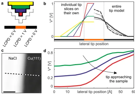
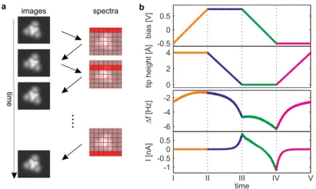
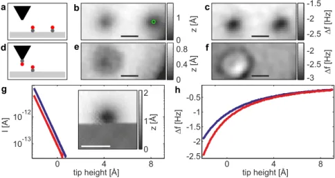
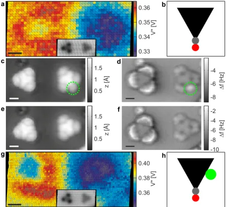
In this regime, KPFS maps have shown a contrast inversion [10] which hints that they may not reflect the charge distribution anymore [10].. Here we study

Here we show by a combination of angle-resolved photoemission (ARPES), scanning tunneling microscopy (STM), and atomic force microscopy (AFM) that the protection mechanism of

Assuming a linear relationship between lateral distortion and force, atomic force microscopy images could be deskewed for different substrate systems.. DOI:

The direct correspondence between the experimental STM images and the molecular orbitals of the free molecule clearly demonstrates that the electronic decoupling pro- vided by

Left: A magnetic atom that is directly evaporated on a metal surface is subject to strong interactions with the substrate, mainly electron scattering leading to a suppression of
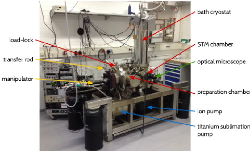
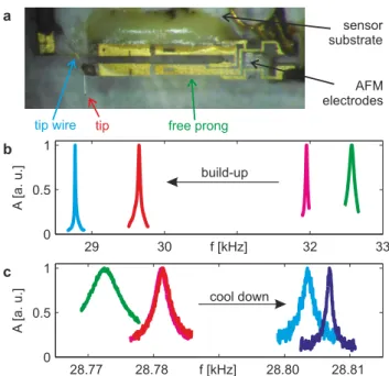
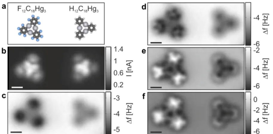
Scanning probe methods like scanning tunneling microscopy STM and atomic force microscopy AFM are the tools of choice for investigating the fundamental electronic, magnetic

While in the past zero-bias anomalies have usually been interpreted as Kondo resonance in the strong anitferro- magnetic (AFM) coupling regime, our analysis of the temperature

It is interesting to note that the corner atoms of a silicon cluster which is bounded by (111) planes must expose two dangling bonds per corner atom, unless one of the (111) planes