Magnetic properties of spin waves in thin yttrium iron garnet films
A. Talalaevskij,1M. Decker,1J. Stigloher,1A. Mitra,2H. S. K¨orner,1O. Cespedes,2C. H. Back,1and B. J. Hickey2
1Department of Physics, University of Regensburg, Regensburg 93053, Germany
2Institute of Materials Research, SPEME, University of Leeds, Leeds LS2 9JT, United Kingdom (Received 14 March 2016; revised manuscript received 31 October 2016; published 10 February 2017) We report spin wave propagation experiments in thin yttrium iron garnet (YIG) films. Using time-resolved scanning Kerr microscopy we extract the mode structure of the spin waves. For quasi-single-mode excitation, the spin wave decay can be fitted with a damped harmonic oscillator function providing us with information about the attenuation length. We measure values of about 2.7 and 3.6μm for the spin wave decay length of 38- and 49-nm-thick YIG samples, respectively. Micromagnetic simulations are performed to compare experimental and simulated modes. The data are in very good agreement with these simulations.
DOI:10.1103/PhysRevB.95.064409 I. INTRODUCTION
Yttrium iron garnet (Y3Fe5O12,YIG) is one of the most widely used materials for studying high-frequency magneti- zation dynamics due to its extremely low Gilbert damping parameter which can reach values as low as 5×10⁻⁵for YIG spheres [1]. Its high Curie temperature and high chemical stability [2] make the material attractive in addition to its interesting magnetic properties. Consequently the material is used for building delay lines, rf filters, attenuators, resonators, Yjunctions and other high-frequency devices [3,4]. Studying spin wave (SW) propagation in thin YIG films and in ultrathin YIG layers has become interesting only lately since high-quality ultrathin YIG films have only become available recently using standard deposition techniques such as liquid phase epitaxy (LPE) [5,6] pulsed layer deposition (PLD) [7–
10], or sputter deposition [11–13]. In particular, the prospect of being able to use sputter deposition, which is the industry standard for thin-film deposition of spintronics devices, to produce high-quality material makes thin YIG films an even more interesting choice for the spintronics community.
In the magnonics community one of the recent fields of research is the quest for using SWs as information carriers.
Experiments concerning SW propagation are important for understanding magnetization dynamics in thin YIG films.
Furthermore, it has been shown that microstructures fabricated from thin YIG films can be used, e.g., to effectively excite auto- oscillations [14,15] by utilizing the spin Hall effect [16–23]
when driving a current through a Pt layer deposited on top of the film. In these experiments thin YIG films are of importance due to their low magnetic moment and exceptionally low damping. Since they are insulators the current density is truly confined to the heavy metal layer.
Thin YIG films are usually grown on gadolinium gallium garnet (GGG) substrates. GGG/YIG bilayers are used because of the lattice parameter proximity (1.2381 nm for GGG and 1.2376 nm for YIG). Usually YIG is grown using LPE, which allows growing high-quality YIG films. LPE-grown films are very homogeneous, have small surface roughness, and low magnetic damping. However, it seems to be difficult to grow thin films with thicknesses much lower than 20 nm. To further reduce the film thickness other methods have been considered.
PLD [24,25] and magnetron sputtering allow growing very thin layers with quality approaching that of LPE-grown films [26,27].
In this work we investigate thin YIG films grown by sputter deposition by combining static and dynamic magnetic characterization methods. Using superconducting quantum interference device (SQUID) measurements we analyze the magnetic moment as a function of film thickness.
Using ferromagnetic resonance (FMR) and propagating SW spectroscopy we investigate the dynamic properties and in particular the damping behavior of thin YIG films and thin YIG microstructures. We report time-resolved magneto-optic Kerr (TRMOKE) effect measurements of SW parameters in thin YIG films. The mode structure of the SWs is studied as a function of the external magnetic field, thickness, and width of the stripe. We are able to detect a SW signal for distances up to 150μm away from the exciting coplanar waveguide (CPW) for narrow 2-μm-wide stripes. However, the detailed structure of the SW modes is better observed on broader (12–14μm wide) stripes. We calculate the SW attenuation length for the first excited mode for 49- and 38-nm-thick samples.
Furthermore we study the dependence of the maximal SW propagation length as a function of stripe width.
II. SAMPLE PREPARATION AND CHARACTERIZATION YIG films are grown on 0.5-mm-thick single-crystalline cubic gallium gadolinium garnet (GGG) substrates with (111) orientation by magnetron sputtering. Sputtering is performed in an argon and oxygen atmosphere, with a sputtering rate of about 1.74 nm/min. The base pressure is 2.6×10⁻⁸mbar.
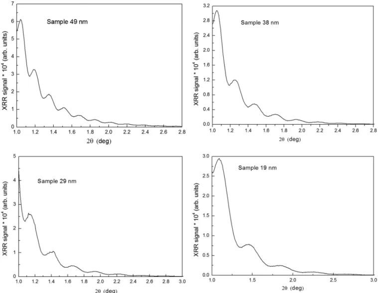
During the deposition at 2.9×10⁻³mbar, the proportion of the sputtered gases oxygen and argon is 5%. Subsequently, the samples are annealed in air for 2 h at 850◦C and slowly cooled to avoid any strain in the film. We investigated four samples with thicknesses of 19, 29, 38, and 49 nm. The thickness of all samples is determined by x-ray reflectivity (XRR) leading to a thickness error less than 1 nm for each sample. Results of the XRR reflectivity measurements after the annealing process are shown in Fig.1. Fitting of the Kiessig fringes allows extracting the film thickness. Before patterning the structures we perform SQUID and FMR measurements to determine the saturation magnetizationMs and the Gilbert damping constantαof the films. The magnetization is measured using SQUID magne- tometry. In Fig.2we present the SQUID data for all samples measured at room temperature (T =300 K). We would like to note that each sample shows a 4–6-nm thick nonmagnetic dead
FIG. 1. X-ray reflectivity dependence on the incidence angle, for different thicknesses after annealing.
FIG. 2. SQUID magnetization loops measured at room tempera- ture (T =300 K) for all samples.
FIG. 3. Dependence of the FMR frequency on the resonance field for a 38-nm-thick sample. The inset shows a typical FMR data set measured using lock-in detection, thus showing the derivative of the Lorentzian absorption line (f =6 GHz). Data measured at room temperature.
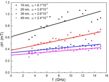
FIG. 4. FMR linewidth as a function of frequency measured at room temperature for all the samples. The solid lines are linear fits to the data.
layer [28]. This layer is formed due to diffusion of the gadolinium from the substrate to the YIG film and needs to be taken into account when calculating the effective magnetic sample volume.
The saturation magnetizationμ0Msat room temperature is found to be around 163 mT for the 49-nm-thick sample and decreases to about 99 mT for the 19-nm-thick sample. For thinner samples the magnetization drops further (for 10-nm- thick samplesμ0Ms ∼75 mT). The relative error in magnetic moment measurement is about 1%. The error in the magneti- zation measurements varies from 7% to 13% depending on the sample thickness, where the biggest relative error comes from the volume measurements. Next we perform in-plane FMR measurements from which we extract the dependence of the resonance field as a function of frequency, see Fig.3, which enables us to extract the effective magnetizationMeff as well as the gyromagnetic ratioγ. Effective magnetization is a sum of saturation magnetization and anisotropy field. Therefore effective magnetization takes the out-of-plane anisotropy into
TABLE I. Magnetic parameters of the thin YIG films.
19 nm 29 nm 38 nm 49 nm
α×10−4 8±2 5.8±0.7 2.6±0.3 2.4±0.3 H0(mT) 0.6±0.06 0.4±0.03 0.3±0.01 0.3±0.01 μ0Ms(mT) 100±12 140±20 150±10 160±10 μ0Meff(mT) 209±1 222±1 227±1 237±0.5 Ku1(J/m3) 4300±500 4600±400 4500±300 4800±300 γ(GHz/T) 28.6±0.6 28.8±0.4 29.0±0.3 28.9±0.1
account. By comparingMeff toMs measured by SQUID, we can compute the perpendicular anisotropy constantKu1. The dependence of the FMR frequency on magnetic field is fitted with the Kittel formula
f = μ0γ
H(H+Meff), (1) which gives us a value of 227 mT forMefffor a 38-nm sample.
We calculate the anisotropy constant as follows:
Ku1= μ0HanisMs
2 = μ0(Meff−Ms)Ms
2 . (2)
In Fig. 4 the results of the FMR measurements of the films with respect to the evolution of the linewidth are shown. In particular we show the dependence of the FMR linewidth on frequency. Since Gilbert damping should be strictly proportional to frequency while the zero-frequency offset is related to extrinsic contributions to damping, such as sample inhomogeneities and two-magnon scattering, linear fits of the dependence of the FMR linewidth on frequency give us information about the Gilbert damping parameter.
The results of the SQUID and FMR measurements are presented in TableI. Here H0 denotes the zero-frequency intercept of the FMR linewidth extracted from linear fits to the data shown in Fig.4, whileαis extracted from the slope of the linear fits to the data. Theαvalues for 38- and 49-nm films are close to the literature value for thin LPE-grown films [29]. Films with thicknesses above 1μm (bulk) [18] can reach values as low as 6.7×10⁻⁵.
FIG. 5. The spin pumping measurements on the 40-nm YIG sample. Dependence of the linewidth on resonance frequency was measured in order to extract Gilbert damping. The solid lines are linear fits of the data.
FIG. 6. A typical view of the sample layout. SWs are excited by the rf field of the CPW. The laser is focused on the YIG stripe and the sample is scanned using a piezostage. The directions of the bias and rf excitation fields correspond to the Damon-Eshbach SW geometry.
As a next step the samples are patterned into stripes for time-resolved magneto-optical Kerr microscopy (TRMOKE) experiments. First thin multilayers (Ti 3 nm/Au 8 nm) are deposited on top of the YIG films. These layers are required for laser beam focusing and increasing the reflectivity of the surface. However, the presence of these metal layers causesα to increase by a factor of about 10 for the 50-nm-thick sample due to efficient spin pumping into Ti which we will briefly discuss below.
In order to prove if the increase in damping indeed stems from spin pumping we perform comparative measurements of Ti/YIG, and Ti/Au for a film with YIG thickness of 40 nm. The data are summarized in Fig.5. As a first step, the 40-nm YIG
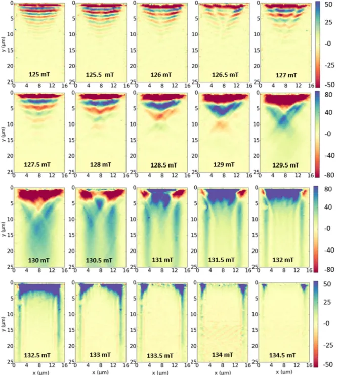
FIG. 7. MOKE images recorded on the 14-μm-wide stripe of the 49-nm-thick YIG sample.
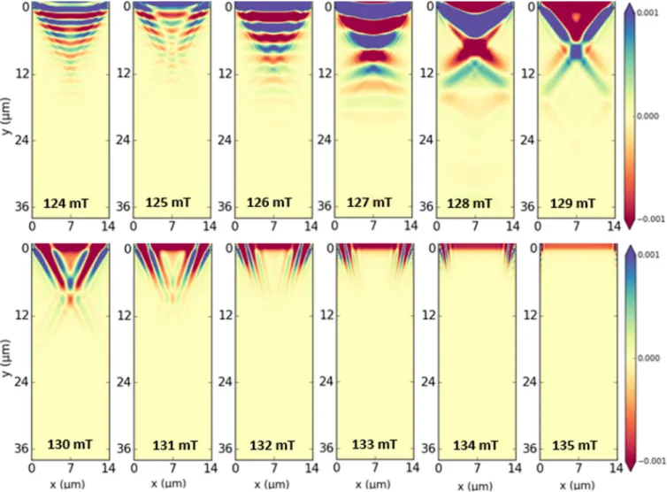
FIG. 8. Simulations of the SW excited by a CPW for the 14-μm-wide stripe.
sample was cut into four pieces marked as s1, s2, s3, and s4 in the Fig.5. Then samples s2 and s4 were covered with a 25-nm thick aluminum oxide layer to exclude possible spin pumping.
Samples s1 and s2 were covered with 10 nm of Ti and samples s3 and s4 with 10 nm of Au. After each step the damping parameter was measured. Since we observe an increase of damping only for YIG/Ti and since the zero-frequency offset of the linewidth remains the same we conclude that the increase of the frequency-dependent linewidth indeed originates from spin pumping. An evaluation using Eq. (3) with the parameters μ0Ms=152 mT, thicknessd =40 nm, electrongfactorg= 2,μBis the Bohr magneton, leads to a spin mixing conductance of 4.1×10¹⁷m−2, which is approximately three times smaller than for YIG/Pt interfaces [9,13,30].
gsp =μ0Msd(αYIG/Ti−αYIG) gμB
. (3)
For the subsequent TRMOKE measurements we pre- pare stripes by using standard electron-beam lithography techniques. Stripes of different width are etched out of the complete film stack using standard electron-beam lithography and ion-beam etching techniques. The distance between the stripes is 10 μm and their width is varied from 2 to 14 μm. We prepare stripe arrays to be able to analyze the
mode structure of the SWs which depends strongly on the stripe width. The stripes are covered with a 20-nm-thick aluminium oxide layer to separate them electrically from a CPW which is prepared in the last step. The CPW has the following parameters: thicknesst =150 nm; signal line width ws=2μm; gap wg=1.5μm. Its impedance is matched to 50.
III. EXPERIMENTAL RESULTS
The experimental setup is conventional TRMOKE, where the Kerr signal is proportional to the dynamic out-of-plane magnetization component (polar MOKE) [31]. The light source is a pulsed titanium sapphire laser operating at a central wavelengthλc=830 nm. Its frequency is doubled in a BBO crystal since the magneto-optical sensitivity depends crucially on the wavelength of the probing beam. In the case of YIG, the magneto-optical response for blue light (λc=415 nm) is about one order of magnitude larger than for red light.
We then synchronize the 80-MHz repetition rate of the laser system to the microwave generator used for rf excitation. The continuous-wave rf excitation is sent into the CPW where the rf current produces the magnetic excitation field. The phase locking enables time-resolved measurements of SWs at a
FIG. 9. Simulations of the edge modes excited by a homogeneous transverse field for the 14μm stripe.
constant phase which can be adjusted using a microwave delay.
The measurements are performed in imaging mode: for a fixed magnetic field and excitation frequency the spatial distribution of the signal is measured. The experimental geometry is shown in Fig.6.
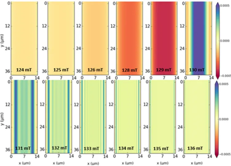
In Fig. 7 we present images of SW excitations recorded for different magnetic fields on the 14-μm-wide stripe. The frequency is fixed at 6 GHz and the magnetic bias field applied along the short axis of the stripe is swept in steps of 0.5 mT. The excitation antenna is located at the top of the images. Distinct SW excitation spectra can be clearly observed as a function of external magnetic field. In the magnetic field region around 125.5 mT a single-SW mode seems to be traveling through the film while at higher fields (e.g., 126.5 mT) it is obvious that the observed SW pattern comprises a superposition of SW modes.
At even higher fields starting at around 130.5 mT a pronounced edge mode starts to become dominant. Additional transverse quantization of standing SWs is visible for magnetic fields larger than 131 mT. Note that the strongest SW response to the excitation frequency is visible at 130 mT. The resolution is high enough to perform accurate fitting and to extract the SW parameters.
To support the experimental data we perform micromag- netic simulations using theMUMAX3code [32]. We use the fol- lowing parameters for the simulations:Ms =1.3×10⁵A/m,
Aex = 3.5×10⁻¹²,Ku1=4.79×10³J/m3,α=2.8×10−3. The simulation results are presented in Figs. 8 and 9.
Figure8shows the simulation of the SWs excited by the CPW.
We can see that the mode structure qualitatively matches the experimental data up to a magnetic bias field of 129.5 mT.
Note, however, that the edge mode observed at higher fields is almost absent in the simulations, whereas it has high intensity in the experiment. The presence of this mode was already shown in thicker YIG films by Brillouin light scattering measurements [29]. The reason why this mode appears in our experiments is a spurious transverse magnetic field that is excited by the current that runs in the thin Ti/Au layer that covers the YIG film. This current is excited inductively by the CPW.SONNETsoftware simulations showed the presence of a current which flows in the direction perpendicular to the CPW. The amplitude of this current is approximately 200 times smaller than the initial current in the CPW, and it decreases linearly with the distance from the ground line of the waveguide. The transverse field created by this current should drop linearly with the distance from the CPW as well.
In Fig.9we can see the simulations of the modes excited by a homogeneous transverse field. It is clear that the amplitude of this mode will drop with decreasing of the transverse field.
Thus, the experimentally recorded images of SW in Fig. 7 are a result of the superposition of modes excited directly by
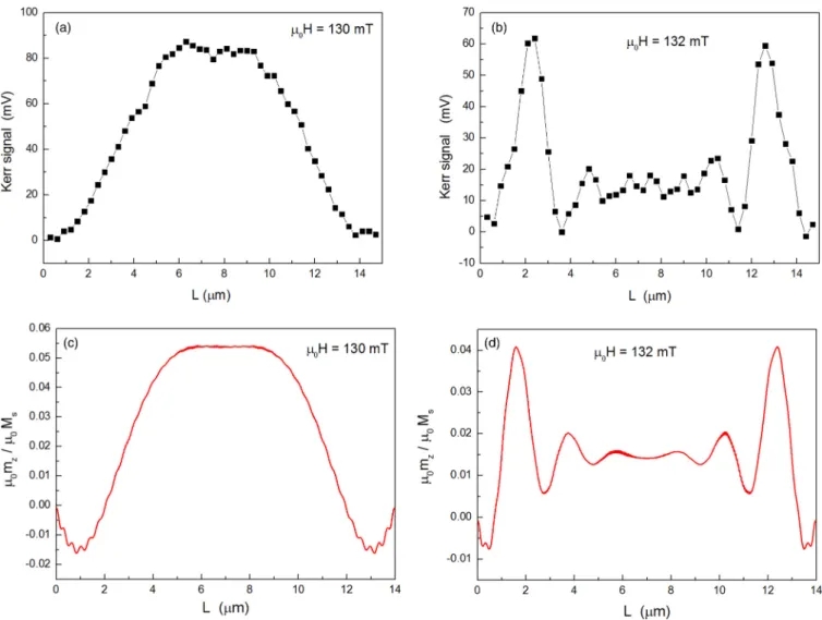
FIG. 10. Line scans in transverse direction of the experimental data (black dots) andMUMAXsimulations (red solid line).
the CPW (Fig. 8) and by the spurious rf field (Fig. 9). We also plot line scans (Fig. 10) of the experimental data and
MUMAX3simulations in transverse directions for two magnetic field values above the 129.5 mT. As we can see the mode structure of the simulation matches the experimental data quite well.
The first image shown in Fig. 7 (recorded at 124 mT) corresponds to the excitation of the first mode withk-vector perpendicular to the CPW; however, at the edges of the stripe the influence of the inhomogeneous internal magnetic field due to demagnetizing effects is clearly observable. With increasing magnetic field the dynamic response of the magnetization slowly transforms to the typical X-shape response (129–
130 mT), a superposition of the first and the third modes with k-vectorsk1andk2, which are also perpendicular to the CPW but have different values. We note here that we can observe SW excitation (mostly carried by the edge modes) [33] in the narrow stripes (<6 μm) at distances exceeding 120μm and reaching values up to 150μm.
The images shown are the X-Y distributions or two- dimensional (2D) arrays of the dynamic out-of-plane magne- tization (zcomponent). If we pick one one-dimensional (1D) array from the 2D array we will get thez(y) distribution for a fixed positionx. This will give us a line scan which can be
fitted with a damped harmonic oscillator function. For the fits we use the following function:
z(y)= Asin (ky+f)e−y/Latt+B. (4) whereLattis the SW attenuation length. The dispersion relation for Damon-Eshbach SWs can be written as follows [1]:
ω2= γ2μ20
H0+Meff 2
2
− Meff
2 2
e−2kd
, (5) where Meff is the effective magnetization, H0 the external magnetic field, d the thickness of the sample, k the wave number, andγ the gyromagnetic ratio. An equation for the group velocity can be obtained from Eq. (5).
vgroup= γ2μ20d Meff2 e−2kd
4ω . (6)
From Eq. (6) the spin wave attenuation lengthLatt can be calculated.
Latt=τ vgroup= μ0γ d Meff2 e−2kd
2αω(Meff+2H0). (7)
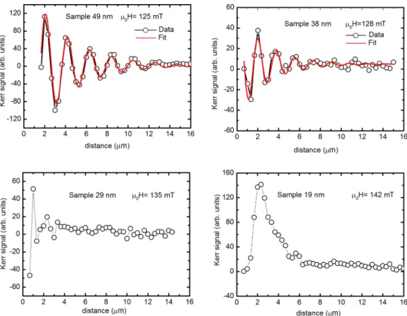
FIG. 11. Dependence of the spin wave amplitude on the distance from the CPW. All measurements are performed for 6 GHz excitation frequency.
FIG. 12. SW imaging at room temperature on the Al (left) and Ti/Au (right) stripes. The field is 160 mT, frequency 6 GHz. The values for the attenuation length obtained from line scans are 2.8±0.3μm for Al and 1.5μm±0.2 for Ti/Au.
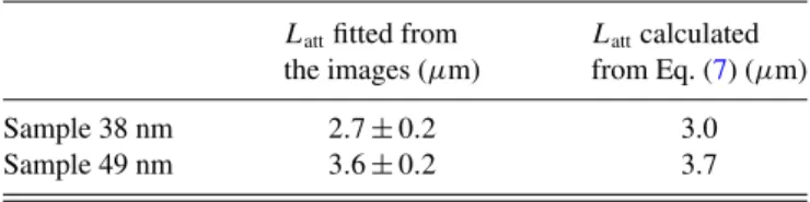
TABLE II. Comparison of the attenuation length determined from SW spectroscopy experiments toLattcalculated fron Eq. (7).
Lattfitted from Lattcalculated the images (μm) from Eq. (7) (μm)
Sample 38 nm 2.7±0.2 3.0
Sample 49 nm 3.6±0.2 3.7
Assuming that for our sample thicknessese−2kd≈1, the attenuation length can be calculated using the SQUID and FMR data. As can be seen from Eq. (7), the attenuation length is proportional to the effective magnetizationMeff and to the sample thicknessd. Taking into account thatMeff drops with the decreasingd, we expect a rapid decrease of the attenuation length with the sample thickness.
In Fig.11line scans for different thicknesses measured at an excitation frequency of 6 GHz are shown. As expected the attenuation lengthLattdrops with decreasing thickness of the sample. For the 29-nm-thick sample the oscillations become aperiodic and for 19 nm are not excited at all.
The results of the fits are presented in Table II and are compared to the values expected from the SW dispersion using the parameter values obtained from the FMR and SQUID data.
As can be observed the results agree well for both samples.
As we have noted above, the use of Ti/Au films for capping is not the best choice since it increases damping due to spin pumping. Note also that this does not change the mode structure of the excited SWs; it just influences their attenuation.
A possible substitute could be the light metal aluminum. To check this we have deposited a stripe of Ti/Au (3 nm/8 nm) and a 20-nm-thick Al stripe onto the same 25-nm sputtered YIG sample to perform comparative measurements. The
widths of the stripes are 12μm. The images and corresponding fitted line scans are presented in Fig.12.
These measurements prove that aluminum is a much better candidate for capping than the Ti/Au bilayer.
IV. CONCLUSIONS
In this paper we presented an analysis of SW propagation experiments in stripes prepared from thin YIG films. A batch of YIG samples of different thicknesses were prepared by magnetron sputtering. Magnetic properties were measured using SQUID and FMR techniques. CPWs for SW excitation were fabricated on top of the films. We performed TRMOKE imaging of the SWs in the thin YIG films and extracted the mode structure of the SWs. For quasi-single-mode excitation we were able to fit the SW decay with a damped oscillator function providing us with information about the attenuation length in the thin YIG film structures for the first SW mode.
MUMAXsimulations were performed to compare experimental and simulated modes. The MOKE data are in very good agree- ment with these simulations. In addition we have performed a comparative measurement of SW propagation on stripes capped with Ti/Au and aluminum. For Al-capped films the decay length increases by roughly a factor of 2. Nevertheless, we are able to observe SW excitations at distances as far as 150 μm from the CPW which is an encouraging result for using SWs in thin sputtered YIG films as information carriers.
ACKNOWLEDGMENTS
The research leading to these results has received funding from the European Union Seventh Framework Programme (FP - People-2012-ITN) under Grant No. 316657 (SpinIcur).
[1] A. G. Gurevich and G. A. Melkov,Magnetization Oscillation and Waves(CRC Press, Boca Raton, FL, 1996).
[2] K.-i. Uchida, T. Kikkawa, A. Miura, J. Shiomi, and E. Saitoh, Phys. Rev. X4,041023(2014).
[3] B. Kaa, VHF Commun.4, 217 (2014).
[4] U. Rohnde, A. Poddar, and G. B¨ock,The Design of Modern Microwave Oscillators for Wireless Applications(Wiley Inter- science, Hoboken, NJ, 2005).
[5] R. Henry, P. Besser, D. Heinz, and J. Mee, IEEE Trans. Magn.
9, 0018 (1973).
[6] J. E. Mee, J. L. Archer, R. H. Meade, and T. N. Hamilton, Appl. Phys. Lett.10,289(1967).
[7] M. C. Onbasli, A. Kehlberger, D. H. Kim, G. Jakob, M. Kl¨aui, A. V. Chumak, B. Hillebrands, and C. A. Ross,APL Mater.2, 106102(2014).
[8] O. d’Allivy Kelly, A. Anane, R. Bernard, J. Ben Youssef, C.
Hahn, A. H. Molpeceres, C. Carr´et´ero, E. Jacquet, C. Deranlot, P. Bortolotti, R. Lebourgeois, J.-C. Mage, G. de Loubens, O.
Klein, V. Cros, and A. Fert, Appl. Phys. Lett. 103, 082408 (2013).
[9] B. Heinrich, C. Burrowes, E. Montoya, B. Kardasz, E. Girt, Y.-Y.
Song, Y. Sun, and M. Wu,Phys. Rev. Lett.107,066604(2011).
[10] Y. Sun, Y.-Y. Song, H. Chang, M. Kabatek, M. Jantz, W. Schneider, M. Wu, H. Schultheiss, and A. Hoffmann, Appl. Phys. Lett.101,152405(2012).
[11] Y.-M. Kang, S.-H. Wee, S.-I. Baik, S.-G. Min, S.-C. Yu, S.-H.
Moon, Y.-W. Kim, and S.-I. Yoo, J. Appl. Phys.97, 10A319 (2005).
[12] T. Liu, H. Chang, V. Vlaminck, Y. Sun, M. Kabatek, A.
Hoffmann, L. Deng, and M. Wu,J. Appl. Phys.115,17A501 (2014).
[13] S. R. Marmion, M. Ali, M. McLaren, D. A. Williams, and B. J.
Hickey,Phys. Rev. B.89,220404(2014).
[14] A. Hamadeh, O. d’Allivy Kelly, C. Hahn, H. Meley, R. Bernard, A. H. Molpeceres, V. V. Naletov, M. Viret, A. Anane, V. Cros, S. O. Demokritov, J. L. Prieto, M. Mu˜noz, G. de Loubens, and O. Klein,Phys. Rev. Lett.113,197203(2014).
[15] V. E. Demidov, S. Urazhdin, H. Ulrichs, V. Tiberkevich, A. Slavin, D. Baither, G. Schmitz, and S. O. Demokritov, Nat. Mater.11,1028(2012).
[16] Y. K. Kato, S. M¨ahrlein, A. C. Gossard, and D. D Awschalom, Science306,1910(2004).
[17] J. Wunderlich, B. Kaestner, J. Sinova, and T. Jungwirth, Phys. Rev. Lett.94,047204(2005).
[18] T. Jungwirth, J. Wunderlich, and K. Olejnik,Nat. Mater.11,382 (2012).
[19] T. Kimura, Y. Otani, T. Sato, S. Takahashi, and S. Maekawa, Phys. Rev. Lett.98,156601(2007).
[20] S. Murakami, N. Nagaosa, and S.-C. Zhang,Science301,1348 (2003).
[21] S. Murakami, N. Nagaosa, and S.-C. Zhang,Phys. Rev. Lett.93, 156804(2004).
[22] T. Tanaka, H. Kontani, M. Naito, T. Naito, D. S. Hirashima, K.
Yamada, and J. Inoue,Phys. Rev. B77,165117(2008).
[23] K. Ando and E. Saitoh,J. Appl. Phys.108,113925(2010).
[24] Y. Sun, H. Chang, M. Kabatek, Y.-Y. Song, Z. Wang, M. Jantz, W. Schneider, M. Wu, E. Montoya, B. Kardasz, B. Heinrich, S. G. E. te Velthuis, H. Schultheiss, and A. Hoffmann.
Phys. Rev. Lett111,106601(2013).
[25] M. B. Jungfleisch, A. V. Chumak, A. Kehlberger, V. Lauer, D. H.
Kim, M. C. Onbasli, C. A. Ross, M. Klaui, and B. Hillebrands, Phys. Rev. B91,134407(2015).
[26] V. Castel, N. Vlietstra, B. J. van Wees, and J. Ben Youssef, Phys. Rev. B90,214434(2014).
[27] R. C. Linares, R. B. McGraw, and J. B. Schroeder,J. Appl. Phys.
36,2884(1965).
[28] A. Mitraet al.(private communication).
[29] P. Pirro, T. Br¨acher, A.V. Chumak, B. Lagel, C. Dubs, O.
Surzhenko, P. G¨ornet, B. Leven, and B. Hillebrands,Appl. Phys.
Lett.104,012402(2014).
[30] Z. Qiu, K. Ando, K. Uchida, Y. Kajiwara, R. Takahashi, H.
Nakayama, T. An, Y. Fujikawa, and E. Saitoh,Appl. Phys. Lett.
103,092404(2013).
[31] J.-Y. Chauleau, H. G. Bauer, H. S. K¨orner, J. Stigloher, M.
H¨artinger, G. Woltersdorf, and C. H. Back,Phys. Rev. B89, 020403(R) (2014).
[32] A. Vansteenkiste, J. Leliaert, M. Dvornik, M. Helsen, F. Garcia- Sanchez, and B. Van Waeyenberge,AIP Adv.4,107133(2014).
[33] G. Duerr, K. Thurner, J. Topp, R. Huber, and D. Grundler, Phys. Rev. Lett.108,227202(2012).