Conductance anomalies of CoFeB/MgO/CoFeB magnetic tunnel junctions
S. Ringer,1,2,*M. Vieth,2L. B¨ar,2M. R¨uhrig,2and G. Bayreuther1,†
1Institut f¨ur Experimentelle und Angewandte Physik, Universit¨at Regensburg, 93040 Regensburg, Germany
2Siemens AG, Corporate Technology, 91050 Erlangen, Germany
(Received 7 August 2012; revised manuscript received 27 September 2014; published 3 November 2014) TheI-V characteristics of CoFeB/MgO/CoFeB magnetic tunnel junctions show pronounced nonlinearities which are relevant both for sensor applications and for the basic understanding of spin-dependent tunneling. To study the relation between the tunnel characteristics and the tunnel magnetoresistance (TMR) ratio, a series of CoFeB/MgO/CoFeB junctions was annealed with stepwise increasing annealing time at different temperatures.
The related TMR ratio and theI-V characteristics were measured in the temperature range between 15 K and 300 K. This allowed the comparison ofI-V characteristics of the same junction for TMR ratios between 25%
and 150% at 300 K thus eliminating the influence of variations in the preparation process of separate individual samples. In addition to a zero bias anomaly observed in particular at low temperatures and for large TMR ratios, a conductance anomaly in theI-V curves was observed around a bias voltage of 350 mV. A general correlation between the deviation from Ohmic I-V characteristics and the TMR ratio was found both for parallel and antiparallel magnetizations of both ferromagnetic layers. This means that the shape of theI-V curves directly scales with the spin polarization of the tunneling current and the proportion of coherent electron tunneling.
Both the 350 mV conductance anomaly and the correlation between non-Ohmic characteristics and the TMR ratio can be explained by considering the contributions of the relevant majority and minority spin bands of the ferromagnetic contacts.
DOI:10.1103/PhysRevB.90.174401 PACS number(s): 72.25.−b,73.40.Gk,85.70.Kh
I. INTRODUCTION
Magnetic tunnel junctions (MTJs), i.e., two ferromagnetic films separated by a thin insulating barrier layer, which show the tunnel magnetoresistance (TMR) effect, have been extensively studied due to their wide applications in a variety of spintronic devices like magnetic field sensors in hard disk drives, and as nonvolatile magnetic memories or mi- crowave nano-oscillators. The TMR ratio is defined as TMR= (RAP−RP)/Rp, whereRP (RAP) are the resistance values for the parallel [P](antiparallel [AP]) magnetization state of the two ferromagnetic layers. The origin of the difference in resistance between the P and AP state is the spin dependence of the tunneling probability of electrons and, hence, the spin polarization of the tunneling current through the barrier [1].
Early experiments with MTJs mostly used amorphous AlOx as a barrier material. These types of MTJs could be described with Julliere’s model [2], which is based on the total electron spin-polarization at the Fermi level. In this model, the maximum possible TMR ratio is limited by the spin-polarization of the electrode material and amounts to values of up to 70% for typical metallic ferromagnets [3].
Higher TMR ratios were first predicted [4,5] and then experimentally confirmed [6,7] for single-crystalline MgO barriers with crystalline electrodes. In contrast to amorphous AlOx barriers, tunneling in this system is coherent, the sym- metries of the Bloch electron wave functions are conserved, and evanescent states of tunneling electrons need to couple with electronic states in the barrier of the same symmetry and energy. The decay rate of the respective states in the barrier
*Sebastian.Ringer@ur.de
†Guenther.Bayreuther@ur.de
determines the tunneling probability; thus, the barrier acts as a symmetry-filter. For the system of Fe/MgO/Fe, this means that the majority electronic states of 1 symmetry have by far the highest tunneling probability, leading to a nearly 100%
spin-polarized tunneling current in ideal MTJs. In theory, this enables TMR ratios larger than 1000% [5]. Similar predictions were made for the system of CoFe/MgO/CoFe [8].
Surprisingly, the highest TMR ratios have been observed in MTJs with amorphous CoFeB electrodes grown by sputtering.
However, postdeposition annealing turned out to be crucial for achieving “giant” TMR ratios of 230% [9], later even above 600% [10] at room temperature, and more than 1000% at 5 K [10,11]. CoFeB grows amorphous when sputtered, while MgO grows polycrystalline beyond five atomic layers with a pronounced (001) out-of-plane texture [12]. During annealing, boron from the CoFeB layer is assumed to diffuse away [13,14], and layers of FeCo(100) crystallize at the MgO(100) interface, with the MgO serving as a template for FeCo(100) grains. Theoretical studies have indicated that a single atomic layer of crystalline Fe at the interfaces of a crystalline MgO barrier should be sufficient to achieve a giant TMR ratio [15]. Heat treatment also enlarges the grain size and reduces defects in the MgO barrier [16], supposedly contributing to the observed increase of the TMR ratio.
The kinetics of the processes occurring during annealing have been studied in detail [17–19]. Specific useful infor- mation has been obtained from the time evolution of the TMR ratio during annealing. In particular, it was shown by in situsynchrotron-based x-ray diffraction that for annealing at 420◦C the gradual increase of the TMR ratio is primarily related to a progressive crystallization of the CoFeB electrodes [18]. However, in these studies the effect of annealing on the I-V characteristics was not considered. The TMR ratio is known to have its maximum at very low bias voltage and to
decrease with increasing bias. For the CoFeB/MgO/CoFeB MTJs studied in the present experiment, the bias voltage for a 50% reduction of the TMR ratio compared to the maximum at low bias,V1/2, is around 300–400 mV. Optimization of MTJs, e.g., for applications as magnetic field sensors, therefore, requires a compromise between a large TMR ratio and a large enough voltage signal in order to obtain the maximum signal- to-noise ratio. A systematic optimization procedure makes it necessary to know theI-Vcharacteristics for the parallel and antiparallel state of the MTJ. Hence, understanding the mecha- nism behind the bias dependence of MTJs is an important step to improve their properties required for practical applications.
Furthermore, studying the effect of annealing on theI-V char- acteristics might help to discriminate between several conceiv- able mechanisms. Several groups [20–22] have reported mod- ifications of theI-V characteristics by annealing at particular temperatures, but the gradual evolution with annealing time ofI(V) together with the TMR ratio for various temperatures has not been studied quantitatively so far. It is the aim of the present paper to investigate the time dependence ofI(V) during annealing at different temperatures and correlate it with the time evolution of the TMR ratio. It is expected that this will lead to a deeper understanding of the bias dependence of the TMR ratio in general and of the underlying processes occurring during annealing of CoFeB/MgO-based MTJs in particular.
Several effects are known to affect the bias dependence of the differential conductance, G(Vb)=dI /dVb, in tunnel junctions: the electronic band structure of the electrodes and the barrier [22–27], defect scattering [28,29], magnon scattering [20,25,26,30–34], and phonon scattering [25,33,35].
Two different anomalies have been reported as showing up as a nonmonotonic behavior of G(Vb). (i) A so-called zero bias anomaly (ZBA), seen as a dip ofG(Vb) around Vb=0 at low temperatures [21,24,26,30,32,33,36], is controversially interpreted either as signature of magnetic impurity scattering corresponding to the Kondo effect [32], in particular by magnetic impurity scattering in the MgO barrier [36], or as a consequence of electron-electron scattering at disordered interfaces [21], or due to magnon excitations [24,30,31].
(ii) A second anomaly around ±350 mV was also observed [20,21,22,24,25,32] and related first to the electronic band structure of MgO [32] and later more specifically to certain features of the band structure of the ferromagnetic electrode [21–25]. A similar anomaly around ±200 mV observed in Fe/MgO/Fe MTJs has been explained with the role of the5 majority band [23].
The interpretation of the respective anomaly in CoFeB- based MTJs around 300–350 mV has been controversial: while in Ref. [22], the CoFe5 and2 bands are ruled out from causing the anomaly, other authors suggest the5majority or the 1 minority band to be the origin of this anomaly [21], or minority states with5symmetry [25]. This point will be discussed further below.
Although in Ref. [24] the effect of annealing on the anomalies was not explicitly investigated, a gradual decrease of the amplitude of the ZBA by a 1 hour anneal at increasing temperatures (200◦C, 250◦C, 300◦C) was found in Ref. [21], but the kinetics of the ZBA and the 350 mV anomaly during annealing were not investigated. It is the intention of the present paper to study the evolution in time of the I-V
characteristics of CoFeB/MgO/CoFeB MTJs by annealing at different temperatures in order to identify a possible correlation between the crystallization and diffusion kinetics responsible for the increasing TMR ratio and the peculiar features of the I-V characteristics. A particular procedure was adopted, which consists of consecutive annealing steps on identical samples. This allows us to avoid the influence of vari- ations of substrate and growth conditions, which are inevitable if MTJs with different TMR ratio are fabricated separately.
In the experiment, we found a universal correlation between the deviation from Ohmic behavior in theI-V characteristics and the TMR ratio, meaning that the I-V characteristics is directly related to the proportion of coherent electron transport irrespective of the particular preparation conditions of the individual MTJs. This could be explained based on the electronic band structure of the ferromagnetic electrodes.
II. EXPERIMENT
Magnetron sputtering was used to fabricate MTJs on thermally oxidized silicon wafers with a layer sequence of (top to bottom) CoFeB(2 nm)/MgO(1.5 nm)/
Mg(0.6 nm)/CoFeB(4 nm)/Ru(0.8 nm)/Co75Fe25(2.5 nm)/
PtMn(25 nm) using a sputtering target of Co60Fe20B20
for the CoFeB layers. The use of a 0.6-nm-thick Mg layer next to the barrier is expected to absorb diffusing oxygen [25,37]. The synthetic antiferromagnet CoFeB(4 nm)/Ru(0.8 nm)/Co75Fe25(2.5 nm) together with the antiferromagnet PtMn(25 nm) constitutes the pinned reference layer. Using photolithography and ion-beam milling techniques, junctions of 3×24μm2 were microfabricated.
The shape induces a pronounced in-plane magnetic anisotropy that ensures well-defined parallel and antiparallel magnetic states even when no exchange bias with the antiferromagnet has yet been established. As a result, P and AP states could be safely switched even in as-deposited junctions (prior to any annealing step).
Annealing was done in a N2 and He flooded box at temperatures of 200◦C, 250◦C, 300◦C, and 350◦C. At each temperature, a set of four as-deposited MTJs were annealed, making a total of 16 MTJs used in this experiment. Each MTJ was always annealed at the same temperature. To study the evolution of the MTJ properties with increasing annealing time, the annealing process was done step by step with TMR andI-V measurements between the steps. Experimental data shown in the subsequent figures refer to individual junctions, except as will be seen in Fig. 8, which compiles the data for all 16 junctions.
The annealing time for each step was chosen empirically to produce a modest increase of the TMR value, which meant longer annealing times for lower temperatures (one step up to 6 hours) and shorter times for higher temperatures (10 minutes for the shortest). There were seven annealing steps for each junction. For a precise control of the annealing times, the samples were placed on a preheated hot plate at the beginning of each annealing step. At the end of the annealing time, the wafer was put in close contact with a cool Al bar. A constant magnetic field of 0.5 Tesla along the long axis was applied during the entire annealing and cooling process.
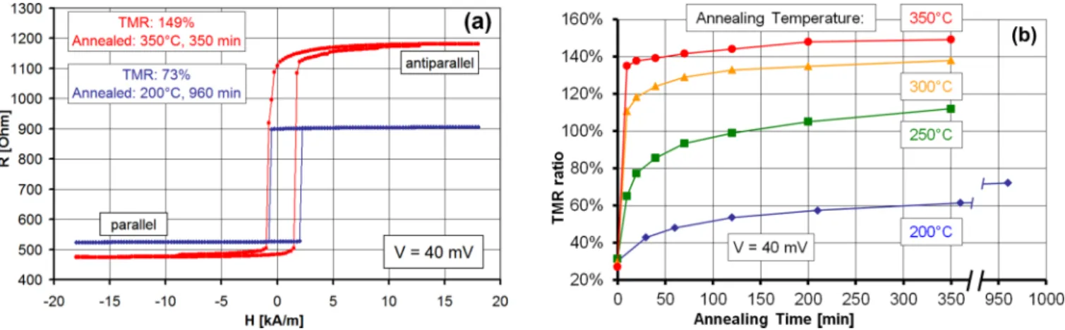
FIG. 1. (Color online) (a) Room temperature magnetoresistance curvesR(H) after annealing at 200◦C and at 350◦C. (b) The evolution of the TMR ratio during annealing at different temperatures for four as-prepared MTJs. The TMR ratio was measured atV = 40 mV.
The lowest annealing temperature of 200◦C was empir- ically chosen as the temperature at which annealing for a reasonable time started to increase the TMR ratio. The temperature of 350◦C was the highest technically accessible.
TheI-V measurements were performed at a probe station with a four-point dc measurement at room temperature using a Keithley 2400 sourcemeter. Before an I-V measurement, magnetoresistance curvesR(H) were measured [see Fig.1(a)]
to determine the magnetic field values required to switch between the P and the AP state.
III. RESULTS AND DISCUSSION
Figure 1(a) shows two typical magnetoresistance curves R(H) measured with a bias voltage ofV = 40 mV at room temperature. The higher TMR ratio of 149% after annealing at 350◦C compared to the 200◦C anneal with a TMR ratio of 73% results from both a lowerRAand a higherRAP. This behavior was observed for all junctions.
The typical evolution of the TMR ratio with annealing time for different annealing temperatures is shown in Fig. 1(b);
the four MTJs shown are representative of the total of 16 junctions studied. The variation in TMR is less than 3% for MTJs that were subject to the same annealing procedure. A rapid increase of the TMR ratio is seen at the beginning, in particular for annealing temperatures of 300◦C and above, followed by a slower increase. The same behavior has been reported by Wanget al.before [17]. In a subsequent paper [18], these authors studied the kinetics of crystallization processes by x-ray diffraction and electron microscopy and identified the crystallization of CoFeB in an inhomogeneous solid-state epitaxy mode. By combining the time evolution of CoFeB crystallization with spin-dependent coherent tunneling, which is strongly affected by the defect density in the MgO barrier, they later attempted to quantitatively separate the contributions of structural changes in the barrier and the electrodes during annealing [19]. The unknown (time-dependent) defect density and exact concentration of impurities in the MgO barrier precluded a complete separation of relevant microscopic processes, but two contributions were identified: the initial rapid increase of the TMR ratio is mostly due to the fast
crystallization of CoFeB, while the subsequent slow increase is mostly due to the contribution from the MgO barrier [19].
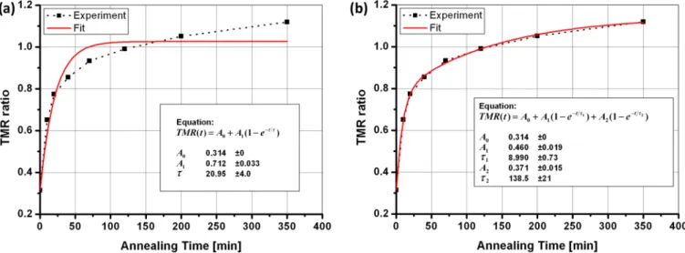
Because a quantitative correlation between the TMR ratio and structural parameters during annealing is not available [19], we use a phenomenological approach based on an exponential time dependence typical of relaxation phenomena.
Assuming just a single relaxation timeτ for the increase of the TMR ratio according to
TMR(t)=A0+A1(1−e−t/τ)
does not give a reasonable fit to the experimental data, as seen in Fig.2(a). The assumption of two relaxation processes with different time constants according to
TMR(t)=A0+A1(1−e−t/τ1)+A2(1−e−t/τ2), however, allows us to fit the data of all 16 MTJs quite well; one example of this is shown in Fig.2(b). This means that the annealing behavior is governed by at least two different processes, in agreement with the interpretation of Wang et al. [19]. While the fast process can be identified with the crystallization of the CoFeB electrodes, an explicit discrimination between the effects of lattice defect density and impurity concentration in the MgO layer related to the slow process is not possible at present [19]. Nevertheless, our observations agree with the detailed investigation of the annealing kinetics by Wang et al. [19], including nearly the same TMR ratio after comparable annealing time and temperature. This ensures that discussing the evolution of the I-V characteristics during annealing in the following refers to typical intrinsic properties of CoFeB/MgO/CoFeB MTJs. Furthermore, knowing how the TMR ratio evolves with annealing temperature and time allowed us to prepare MTJs with a specific TMR value obtained by different annealing procedures, i.e., either by a long anneal at a low temperature or a shorter anneal at a higher temperature. This will be essential for the interpretation of non-Ohmic tunnel characteristics below. Before, we discuss the bias dependence of typicalI-V curves.
The bias dependence of the MTJs was measured at every data point (four MTJs per data point) during the annealing procedure shown in Fig.1(b). The differential resistance (Rd) vs voltage curves is shown in Fig.3for a junction annealed at
FIG. 2. (Color online) (a) Fit of the data from Fig.1(b)for the annealing process at 250◦C using one exponential. (b) Fit of the data from Fig.1(b)using two exponentials.
250◦C [Fig.3(a)] and 350◦C [Fig.3(b)] for both the parallel and antiparallel magnetization of the free and the pinned layer after the first and last annealing step. The data shown are typical for all the MTJs studied here. This differential resistanceRd = dV /dIshows variations of theI-V behavior more clearly than the normal (nondifferential) resistanceR=I /V.
As can be seen in Fig. 3, Rd of both states exhibits a non-Ohmic characteristic, i.e., a strong bias dependence.
In general, Rd decreases with increasing absolute bias, as expected for electron transport by tunneling [38,39]. The decay ofRdwith increasing bias is stronger for the AP configuration than for the P configuration, resulting in a lower TMR ratio at higher bias. As can be seen in Fig. 3(a), the increase in TMR through annealing does not only arise from an increased Rd(AP) but also from a decreased Rd(P). At 350◦C, 10 minutes annealing reduces Rd(P) as well (not shown), but after 350 minutes annealing Rd(P) has slightly increased.
According to Wanget al.[19], this is attributed to diffusion of Mn into the MgO barrier and will eventually lead to a reduced TMR ratio.
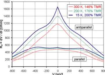
The change ofRd during annealing for both states and its bias dependence are even more pronounced at low temperature.
Figure4shows measurements ofRd(V) at 300 K, 200 K, and 15 K of a sample with 147% TMR at 300 K. At 15 K, two anomalies are clearly discernible: (i) a ZBA can be seen as a sharp tip mainly in the AP state, originating either from magnetic impurity scattering in the MgO barrier [32] (Kondo effect [36]) or from electron-electron scattering at disordered interfaces [21] and (ii) flat local maxima around±350 mV at 15 K mainly in the P state, which result in a flat plateau at higher temperatures (see Fig.3).
The origin of the 350 mV anomaly in CoFeB/MgO MTJs was first supposed to be connected with the electronic band structure of a MTJ with a crystalline barrier/electrode interface
FIG. 3. (Color online) Room temperature differential resistance (Rd=dV /dI) vs voltage of a MTJ for the parallel and antiparallel magnetic states. The solid black lines show the MTJ after the first annealing step of 10 minutes, while the dotted red lines show the same MTJ after the last annealing step resulting in a total annealing time of 350 minutes. The arrows indicate the approximate boundaries of a growing plateau in the P stateRd(V) curve (a) after annealing at 250◦C and (b) after annealing at 350◦C.
FIG. 4. (Color online) Comparison of Rd−U diagrams of a MTJ at temperatures of 300 K, 200 K, and 15 K.
[32], allowing coherent tunneling of electrons. Recently, the origin of this anomaly was discussed by Teixeiraet al.[24] on the basis of the calculated band structure of bulk body-centered cubic (bcc)-Fe and bcc-Co, which is shown in Fig.5.
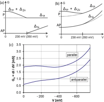
For a Fe/MgO/Fe junction, the current at low bias in the P state is carried mainly by the1 majority spin state1↑ with small contributions from the 5 majority and minority bands,5↑and5↓, and the2minority band2↓, while the contribution from the2majority and minority bands should be negligible due to their extremely strong damping in the barrier [4]. If the bias voltage exceeds a value of about 100 mV, the energy of electrons after coherent tunneling through the barrier is higher than the top of the5and2majority bands;
hence, these bands will not form a coherent conduction channel any longer [23]; therefore, we expect a drop in conductance or an increase of resistance, respectively. A corresponding P state conductance anomalyis therefore expected around 100 mV for a Fe/MgO/Fe MTJ.
FIG. 5. Band diagram of bcc-Fe (a) and bcc-Co (b) spin bands (after Ref. [1]).
In the AP state, the1band will not conduct for low bias, only the5and2states will carry a relatively small current.
Above 1.3 V, the1 minority spin band,1↓, will start to conduct, and an increase of conductance is expected, i.e., a different conductance anomalywill appear in the AP state.
Experimentally for Fe/MgO/Fe epitaxial MTJs, a peak in the tunnel spectra (d2V /dI2vsV) for the AP state slightly above 1000 mV has indeed been observed by Andoet al.[27] and related to the1↓band conductance anomaly just described. In a discussion of this anomaly by Yuasa and Djayaprawira [1], a steplike increase of the tunnel conductance was schematically assumed as soon as the1↓band starts to conduct. The tunnel spectrum, however, shows a broad peak instead of aδ-function [27]. This can be understood by assuming that after crossing the band edge, the tunnel conductance increases gradually from zero instead of a sudden jump because of the growing phase space available. For the same reason, the effect causing the conductance anomaly around 100 mV will show up as a gradual decrease of the conductance until it vanishes when the electron energy exceeds the top of the5 and2 majority bands at about 100 mV.
For bcc-Co, the Fermi level is shifted upwards compared to bcc-Fe, as illustrated in Fig.5(b), in the spirit of a rigid band model. In the P state of a bcc-Co/MgO/bcc-Co MTJ, the current at low bias will again be carried mainly by the1 majority spin band, with a small contribution from the2,5, and2minority spin bands. With increasing bias the electron energy at the interface to the second electrode will excel the top of the2 minority spin band at a value of 230 mV [40].
Consequently, the conductance will drop at this bias value. This effect was regarded as the origin of the conductance anomaly in CoFeB-based MTJs in the P state in Ref. [24]; the shift to higher bias (350 mV instead of 230 mV), which was not discussed by the authors, can be explained by assuming that a Co-rich bcc-CoFe alloy is formed at the interface during the annealing process with the Fermi level lying somewhat below that of bcc-Co according to the rigid band model adopted here.
In the AP state of a bcc-Co/MgO/bcc-Co MTJ, the1band of bcc-Co will not conduct for low bias, and the2,5, and2
bands will not contribute to conduction because the respective majority spin bands are well below the Fermi level; therefore, coherent tunneling is totally suppressed and a markedly higher TMR ratio is expected compared to a MTJ with Fe electrodes [1,8]. The TMR ratio will not approach infinity because an incoherent background conductance will be present in a real junction. However, if the bias voltage exceeds 230 mV, the1 minority spin band will provide a coherent conduction channel, and the total conductivity will increase, thus again producing a conductance anomaly. As mentioned before, for Co-rich CoFeB-based MTJs, the anomaly is expected at somewhat higher bias around 300–350 mV.
For the same reasons discussed above for bcc-Fe, for bcc-Co/bcc-FeCo we expect the shape of both anomalies to correspond to a gradual decrease of conductance below 230 mV/350 mV (P state) or a gradual conductance increase above 230 mV/350 mV (AP state), respectively. This is schematically shown in Fig.6(a) for Co and Co-rich CoFe electrodes. For simplicity, gradual transitions are assumed.
Anomalies in the P and AP state are visible in Fig. 4 at the same voltage, more pronounced at lower temperatures.
FIG. 6. (Color online) Schematic conductance vs bias diagram for (a) only coherent tunneling and (b) coherent tunneling and incoherent tunneling. Assuming bcc-Co electrodes, a conductance anomaly in both the P and AP state is expected at 230 mV, while for Co-rich CoFe electrodes 350 mV is expected. (c) Experimental data from Fig.4forT = 15 K converted to differential conductance.
The same data plotted as differential conductance in Fig.6(c) indeed have a clear similarity to the expected behavior shown in Fig.6(b). The deviation for low bias (V < 200 mV) is due to the ZBA, which is present in the data but not taken into account in the underlying model.
This supports the interpretation of the P state and AP state conductance anomalies as being related to the energies of the 1↓ and the 2↓ band edges and, therefore, disagrees with Ref. [25] where the authors conclude from a qualitative reasoning that most likely the5states are responsible for the conductance anomaly around 300 mV.
The interpretation given above only considers coherent transport. In addition, the relative proportion of incoher- ent transport channels increases with growing temperature (Fig.4), increasing bias voltage and higher disorder (Fig.3).
All these factors lead to a lower TMR ratio and should be closely connected with the distinctness of the 350 mV anomaly (Fig.4).
For technical applications of MTJs, the behavior at room temperature is most important. To test the relevance of the 350 mV anomaly in this case, we define the parameterRd, which describes the deviation from Ohmic I-V behavior of theRd(V) curves for the P and AP states at room temperature in the bias region from 75 mV to 275 mV, i.e., the region of the plateau seen in the P stateRd(V) curve in Fig.3(b):
Rd = Rd(75 mV)−Rd(275 mV) Rd(75 mV) .
A highRd value means a strong bias dependence of the conductance, while a lowRd means more Ohmic behavior.
Rdis equivalent to a normalized second derivatived2V /dI2
FIG. 7. (Color online) Deviation from Ohmic behavior at room temperature expressed byRd of all MTJs after all annealing steps at their corresponding TMR ratios. Full circles (red) are for the AP states and open circles (blue) for the P states. The TMR ratios are calculated from R(H) measurements at 40 mV dc. The data points below 40% TMR represent un-annealed MTJs; corresponding annealing temperatures are 200◦C between 40% and 70% TMR, 250◦C between 70% and 110% TMR, 300◦C between 110% and 140% TMR, and 350◦C between 135% and 150% TMR.
averaged between 75 mV and 275 mV. The lower bound of 75 mV was chosen to minimize the influence of the ZBA;
by choosing an upper bound of 275 mV, it was expected to effectively capture the flattest part of theRd vs V curves in Fig.3, which is related to the 350 mV anomaly, and to exclude the effect of the anomaly in the AP state expected above 350 mV.
Figure7shows a compilation ofRd vs TMR ratio for all measured MTJs after all annealing steps. For each annealing temperature (200◦C, 250◦C, 300◦C, and 350◦C), four MTJs were measured eight times each (as deposited and after each of the seven annealing steps). This makes a total of 16 different MTJs with 256 different TMR ratio values in this diagram.
Two facts are evident from Fig. 7: (i) the I-V curves are always more Ohmic-like in the P state compared to the AP state, and (ii) with increasing TMR ratio the conduction becomes more Ohmic in the P state and less Ohmic in the AP state.
To explain these findings we assume that the total tunneling current consists of two components: (i) a component resulting from coherent tunneling of electrons that is governed by the band structure of the materials involved, and (ii) a component related to incoherent electron transport that can be described by a basic model of quantum mechanical tunneling of free electrons. The differential conductance in the case of incoherent tunneling is Ohmic at a very low bias and approximately parabolic at intermediate voltages (e.g., up to 1–2 V) according to Simmons [38].
The incoherent process is the only one observed in tunnel junctions consisting of polycrystalline electrodes and an amor- phous barrier. In contrast, coherent tunneling requires a well- oriented single-crystalline layer stack. We further assume that with increasing structural quality of a CoFeB/MgO/CoFeB tunnel junction during annealing, the proportion of coherent tunneling increases leading to an increase of the TMR ratio.
In the P state, the coherent tunnel current in a CoFe/MgO/CoFe MTJ with high Co content is carried mainly by the1 majority spin band with small contributions from the 2, 5, and 2 minority spin bands, as illustrated in Fig.5. While theI-V characteristics related to the1↑ band are expected to be roughly Ohmic [41], the2↓conductance produces a negative slope for the conductance vs bias,G(V), between 0 and 350 mV, as sketched in Fig.6(a). This negative slope will compete with the positive slope of the incoherent tunnel conductance present in a non-ideal MTJ, resulting in less bias dependence for the combined conductance, i.e., a more Ohmic I-V curve for a bias below 350 mV in the case of CoFe, as shown in Fig.6(b). As a consequence, the deviation from Ohmic behavior quantified by the parameter Rd in the range between 75 mV and 275 mV will decrease with an increasing proportion of coherent tunneling, i.e., with increasing TMR ratio. This is exactly what is shown in Fig.7 forRdP. For a high proportion of coherent transport, RdP can even become negative, as seen in Fig.4for the 15 K data.
At room temperature, we expect this will also happen at high TMR ratios, e.g., for current record values above 500%. This remains to be checked experimentally.
In the AP state, on the other hand, coherent tunneling is not allowed in a MgO-based MTJ with bcc-Co or Co- rich bcc-CoFe contacts for low bias (below 230/350 mV for Co/CoFe) according to the band structure shown in Fig. 5(b). In this case only incoherent tunneling processes are possible, and the deviation from Ohmic I-V relation, RPd, is the maximum possible. If, however, structural defects lead to electron scattering with spin flip, (quasicoherent) electron transport, as described above for the P state, is again possible. Also, a certain proportion of misoriented grains might be present, which allow local coherent transport via different bands. As a consequence, RdP will be lower than for purely incoherent transport. Annealing increases the crystalline quality and reduces this local coherent transport as well as spin-flip scattering. Therefore,RdP will increase and gradually approach its maximum value for purely incoherent tunneling.
Within this interpretation, both facts concluded from Fig.7—thatI-V curves are always more Ohmic-like in the P state compared to the AP state and that with increasing TMR ratio the conduction becomes more Ohmic in the P state and less Ohmic in the AP state—can be consistently understood as well as the appearance of the 350 mV anomaly, which during annealing becomes more distinct in both the P and AP state, even more so at lower temperatures.
The most remarkable observation in Fig.7is an apparent universal relationshipbetween RdP /AP and the TMR ratio for all junctions with 256 different annealing states which was nota prioriexpected. If two MTJs were annealed to the same TMR ratio, no matter the annealing time or temperature, the deviation from Ohmic behavior expressed by the parameter RP /APd is the same. This finding indicates that the character of the I-V curve is uniquely related to the degree of spin polarization of the tunnel current and, therefore, to the degree of coherent electron transport.
This universal relation between the TMR ratio and theI-V characteristics is expected to be of practical relevance for a variety of sensor applications of MTJs. In particular, in many
cases it is not sufficient to maximize the TMR ratio but rather the signal-to-noise ratio of the sensor signal in a given bias range. The close relation of the I-V characteristics to the band structure of the ferromagnetic electrodes found in this contribution may help in selecting the optimum material for specific applications. Furthermore, the 350 mV conductance anomaly (e.g., seen in Fig.4) can be exploited to get an estimate of the alloy composition at the FeCoB/MgO interface after the annealing process required to achieve a high TMR ratio:
different diffusion constants of Fe, Co, and B will lead to an interface alloy composition, which is a priori unknown but to a large extent determines the TMR ratio and specific features of the I-V characteristics. The bias voltage range of the conductance anomaly—about 230 mV for bcc-Co and about 1.2 V for bcc-Fe—can serve as a rough indication of the actual interface composition, which is very difficult to find out by any other method. For this purpose, detailed measurements of the1 minority band edge by tunneling spectroscopy on the one hand andab initiocalculations of the band structure for a wide range of interface alloy composition on the other would be of great value.
In conclusion, we have shown that theI-V characteristics of CoFeB/MgO/CoFeB MTJs are intimately connected with the band structure and the structural quality of the layer materials. The deviation from Ohmic behavior shows a universal relationship with the TMR ratio and hence with the amount of coherent electron tunneling. In the parallel state, the nonmonotonic tunnel conductance as a function of bias voltage below 350 mV mainly originates from a conductance anomaly, which is a consequence of the position of the2minority spin band in the bcc-CoFe contact material. We also propose that the position of the1 minority spin band is responsible for an anomaly in the AP state, which was not considered for CoFeB-based MTJs previously [24].
Recently it has been reported [42] that electron tunneling in epitaxial FeCo/MgO/FeCo(001) MTJs cannot be completely understood on the basis of the band structure calculated for bulk material like the one shown in Fig. 5, which predicts the highest TMR ratio for pure bcc-Co electrodes. Instead, a 1↓interface state is proposed to cross the Fermi energy with increasing Co content, thus limiting the maximum attainable TMR ratio that is observed around 25% Co. Applying this conclusion to our data, however, does not seem meaningful mainly because the exact structure and the actual alloy composition (here nominally Co75Fe25) at the electrode/MgO interfaces are not known. It is unclear whether such an interface state is formed in our samples; the presence of boron could suppress such a state or shift its energy relative to the Fermi level. A detailed chemical and structural analysis of the interfaces in CoFeB-based MTJs on the atomic level would be required but seems rather difficult to achieve.
For the same reason, earlierab initio calculations of the bias dependence in Fe/MgO/Fe tunnel junctions [41] have only minor relevance for a quantitative interpretation of the present I-V characteristics. By considering only coherent transport, the authors for an ideal junction found nearly perfect Ohmic behavior in the P state, a very low conductance with weak bias dependence in the AP state, and dramatic changes of the conductance if one or both interfaces consisted of a monolayer of FeO. This reflects the strong influence
of interface states. For a fundamental understanding of the present experimental results, calculations of Refs. [25] and [41] should be extended to structural models, which reflect the precise atomic interface configurations evolving during the gradual annealing process. This will remain a serious challenge.
Several open questions deserve further experimental in- vestigation, in particular whetherRPd indeed changes sign for very large TMR ratios of 500% or more and whether the universal relationship between RdP /AP and the TMR ratio persists for such high TMR ratios. The conductance anomalies found in the present work can be qualitatively understood based on the bulk band structure of FeCo alloys within a rigid-band model, but the unknown precise atomic
interface structures of annealed FeCoB/MgO/FeCoB tunnel junctions constitute a serious obstacle to a full understanding of these anomalies based on realistic ab initio calculations of the electronic states and spin-dependent transport at these interfaces.
ACKNOWLEDGMENTS
The TMR layer stack preparation by H. Mai, experimental support with low temperature measurements by J. Vigroux, theoretical support by M. del Valle, and financial support by the Deutsche Forschungsgemeinschaft (SFB 689) are gratefully acknowledged.
[1] S. Yuasa and D. D. Djayaprawira,J. Phys. D: Appl. Phys.40, R337(2007).
[2] M. Julliere,Phys. Lett. A54,225(1975).
[3] D. Wang, C. Nordman, J. M. Daughton, Z. Qian, and J. Fink, IEEE Trans. Magn.40,2269(2004).
[4] W. H. Butler, X.-G. Zhang, T. C. Schulthess, and J. M.
MacLaren,Phys. Rev. B63,054416(2001).
[5] J. Mathon and A. Umerski, Phys. Rev. B 63, 220403(R) (2001).
[6] S. S. P. Parkin, C. Kaiser, A. Panchula, P. M. Rice, B. Hughes, M. Samant, and S.-H. Yang,Nat. Mater.3,862(2004).
[7] S. Yuasa, T. Nagahama, A. Fukushima, Y. Suzuki, and K. Ando, Nat. Mater.3,868(2004).
[8] X.-G. Zhang and W. H. Butler,Phys. Rev. B70,172407(2004).
[9] D. D. Djayaprawira, K. Tsunekawa, M. Nagai, H. Maehara, S. Yamagata, N. Watanabe, S. Yuasa, Y. Suzuki, and K. Ando, Appl. Phys. Lett.86,092502(2005).
[10] S. Ikeda, J. Hayakawa, Y. Ashizawa, Y. M. Lee, K. Miura, H. Hasegawa, M. Tsunoda, F. Matsukura, and H. Ohno,Appl.
Phys. Lett.93,082508(2008).
[11] Y. M. Lee, J. Hayakawa, S. Ikeda, F. Matsukura, and H. Ohno, Appl. Phys. Lett.90,212507(2007).
[12] S. Yuasa, Y. Suzuki, T. Katayama, and K. Ando,Appl. Phys.
Lett.87,242503(2005).
[13] J. J. Cha, J. C. Read, W. F. Egelhoff Jr., P. Y. Huang, H. W.
Tseng, Y. Li, R. A. Buhrman, and D. A. Muller,Appl. Phys.
Lett.95,032506(2009).
[14] H. Kurt, K. Rode, K. Oguz, M. Boese, C. C. Faulkner, and J. M.
D. Coey,Appl. Phys. Lett.96,262501(2010).
[15] M. Gradhand, C. Heiliger, P. Zahn, and I. Mertig,Phys. Rev. B 77,134403(2008).
[16] S. Isogami, M. Tsunoda, K. Komagaki, K. Sunaga, Y. Uehara, M. Sato, T. Miyajima, and M. Takahashi,Appl. Phys. Lett.93, 192109(2008).
[17] W. G. Wang, C. Ni, A. Rumaiz, Y. Wang, X. Fan, T. Moriyama, R. Cao, Q. Y. Wen, H. W. Zhang, and John Q. Xiao,Appl. Phys.
Lett.92,152501(2008).
[18] W. G. Wang, J. Jordan-sweet, G. X. Miao, C. Ni, A. K. Rumaiz, L. R. Shah, X. Fan, P. Parsons, R. Stearrett, E. R. Nowak, J. S.
Moodera, and J. Q. Xiao,Appl. Phys. Lett.95,242501(2009).
[19] W. G. Wang, C. Ni, G. X. Miao, C. Weiland, L. R. Shah, X. Fan, P. Parson, J. Jordan-sweet, X. M. Kou, Y. P. Zhang, R. Stearrett,
E. R. Nowak, R. Opila, J. S. Moodera, and J. Q. Xiao,Phys.
Rev. B81,144406(2010).
[20] Q. L. Ma, S. G. Wang, H. X. Wei, H. F. Liu, X.-G. Zhang, and X. F. Han,Phys. Rev. B83,224430(2011).
[21] J. Bernos, M. Hehn, F. Montaigne, C. Tiusan, D. Lacour, M. Alnot, B. Negulescu, G. Lengaigne, E. Snoeck, and F. G.
Aliev,Phys. Rev. B82,060405(R)(2010).
[22] R. Matsumoto, S. Nishioka, M. Mizuguchi, M. Shiraishi, H. Maehara, K. Tsunekawa, D. D. Djayaprawira, N. Watanabe, Y. Otani, T. Nagahama, A. Fukushima, H. Kubota, S. Yuasa, and Y. Suzuki,Solid State Commun.143,574(2007).
[23] C. Tiusan, F. Greullet, M. Hehn, F. Montaigne, S. Andrieu, and A. Schuhl,J. Phys.: Condens. Matter19,165201(2007).
[24] J. M. Teixeira, J. Ventura, M. P. Fern´andez-Garc´ıa, J. P. Araujo, J. B. Sousa, P. Wisniowski, and P. P. Freitas,Appl. Phys. Lett.
100,072406(2012).
[25] G. X. Miao, K. B. Chetry, A. Gupta, W. H. Butler, K. Tsunekawa, D. D. Djayaprawira, and G. Xiao,J. Appl. Phys.99,08T305 (2006).
[26] S. Nishioka, R. Matsumoto, H. Tomia, T. Nozaki, Y. Suzuki, H. Itoh, and S. Yuasa, Appl. Phys. Lett. 93, 122511 (2008).
[27] Y. Ando, T. Miyakoshi, M. Oogane, T. Miyazaki, H. Kubota, K. Ando, and S. Yuasa, Appl. Phys. Lett. 87, 142502 (2005).
[28] Y. Xu, D. Ephron, and M. R. Beasley,Phys. Rev. B52,2843 (1995).
[29] G. X. Miao, Y. J. Park, J. S. Moodera, M. Seibt, G. Eilers, and M. M¨unzenberg,Phys. Rev. Lett.100,246803(2008).
[30] T. Kubota, Q. L. Ma, S. Mizukami, X. M. Zhang, H. Naganuma, M. Oogane, Y. Ando, and T. Miyazaki,J. Phys. D: Appl. Phys.
46,155001(2013).
[31] S. Zhang, P. M. Levy, A. C. Marley, and S. S. P. Parkin,Phys.
Rev. Lett.79,3744(1997).
[32] R. Matsumoto, Y. Hamada, M. Mizuguchi, M. Shiraishi, H. Maehara, K. Tsunekawa, D. D. Djayaprawira, N. Watanabe, Y. Kurosaki, T. Nagahama, A. Fukushima, H. Kubota, S. Yuasa, and Y. Suzuki,Solid State Comm.136,611(2005).
[33] D. Bang, T. Nozaki, D. D. Djayaprawira, M. Shiraishi, Y. Suzuki, A. Fukushima, H. Kubota, T. Nagahama, S. Yuasa, H. Maehara, K. Tsunekawa, Y. Nagamine, N. Watanabe, and H. Itoh,J. Appl.
Phys.105,07C924(2009).
[34] H.-X. Wei, Q.-H. Qin, Q.-L. Ma, X.-G. Zhang, and X.-F. Han, Phys. Rev. B82,134436(2010).
[35] A. M. Bratkovsky,Appl. Phys. Lett.72,2334(1998).
[36] D. Bang, T. Nozaki, Y. Suzuki, K. Rhie, T.-S. Kim, A. Fukushima, S. Yuasa, E. Minamitani, H. Nakanishi, and H. Kasai,J. Phys.: Conf. Ser.200,052004(2010).
[37] A. T. Hindmarch, V. Harnchana, D. Ciudad, E. Negusse, D. A.
Arena, A. P. Brown, R. M. D. Brydson, and C. H. Marrows, Appl. Phys. Lett.97,252502(2010).
[38] J. G. Simmons,J. Appl. Phys.34,1793(1963).
[39] E. L. Wolf, Principles of Electron Tunneling Spectroscopy (Oxford University Press, New York, 1985).
[40] D. Bagayoko, A. Ziegler, and J. Callaway,Phys. Rev. B27,7046 (1983).
[41] C. Heiliger, P. Zahn, B. Yu. Yavorsky, and I. Mertig,Phys. Rev.
B73,214441(2006).
[42] F. Bonell, T. Hauet, S. Andrieu, F. Bertran, P. Le F`evre, L. Calmels, A. Tejeda, F. Montaigne, B. Warot-Fonrose, B. Belhadji, A. Nicolaou, and A. Taleb-Ibrahimi,Phys. Rev.
Lett.108,176602(2012).