Inductive Method for Measuring the Local Transition Temperature of Thin Tungsten Films
Karoline Schäffner, Godehard Angloher, Dieter Hauff, Franz Pröbst, Wolfgang Seidel
Max-Planck-Institut für Physik, Föhringer Ring 6, 80805 München
Abstract. We report on a method for local transition temperature (Tc) measurements of thin tungsten films operated at temperatures down to 10 mK in a dilution refrigerator. The experimental set-up is designed to study possible inhomogeneities in such films as used in the framework of the CRESST (Cryogenic Rare Event Search with Superconducting Thermometers) dark matter search. The method uses a probe coil which is positioned close to the tungsten sample in order to measure the coil’s change of inductance when the sample changes from the normal to the superconducting state. We have demonstrated that stationary local transition temperature measurements on a tungsten single crystal as well as on thin tungsten films work and allow the study of the local dependence ofTc. We are now preparing a set-up using a slip-stick step-scanner to enable the mapping of theTc-distribution of a superconducting tungsten film in one cooldown.
Keywords: Magnetic measurements, Transition temperature, Tungsten films, Superconductivity PACS: 07.55.Jg, 07.20.Mc
1. INTRODUCTION
The CRESST dark matter search uses superconducting transition edge sensors (TES) made out of thin tungsten films to read out massive dielectric absorbers at tempera- tures of about 10 mK [1], [2]. Some of the tungsten films are produced on sapphire substrates (40 mm diameter, 0.4 mm thickness) and have a thickness of 200 nm. For the performance of the CRESST detectors low values of Tcand steep and smooth transition curves are desirable.
This means that the tungsten transition edge sensors, which after lithography have a size of 450×300 µm2, should not show different crystalline structures (α- or β-phase), film stress, or foreign atoms influencing the transition temperature of the sensor. After evaporation the tungsten films have a diameter of 30 mm. The transi- tion curve of such unstructered films as seen in resistive low-current R(T) measurements reflects only the first su- perconducting path across the full film, not giving any information about local properties. The area of a TES produced afterwards, however, is quite small compared to the one of the full film. To study possible inhomo- geneities in the tungsten films and to have a measure of identifying an optimal spot for the TES, a local and con- tactless measurement of the transition temperature of an area of few mm2is needed. In this article we report on stationary and localTcmeasurements of a tungsten single crystal as well as of a thin tungsten film.
2. EXPERIMENTAL SET-UP
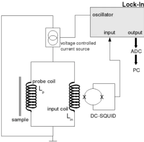
The experimental set-up is based on the fact that the mag- netic susceptibility of tungsten changes when passing from the normal to the superconducting state: In the nor- mal state, tungsten is paramagnetic (χm>0 ), whereas superconducting tungsten behaves like a perfect diamag- net (χm=−1). This is the so-called Meissner-effect dis- covered in 1933 by Meissner and Ochsenfeld [3]. Ac- cordingly, a coil (“ probe coil ”) positioned in close con- tact to the tungsten sample will undergo a corresponding change in inductance. Monitoring this inductance there- fore allows a non-contacting measurement of the transi- tion temperature of the tungsten sample at that area of the sample that is closest to the probe coil. A conven- tional DC-SQUID (Superconducting Quantum Interfer- ence Device) can be used to measure the magnetic flux as a function of temperature down to 10 mK. The tung- sten sample is positioned close to the probe coil which is connected in parallel to the input coil of a SQUID.
The probe coil is chosen to have the same inductance as the input coil of the DC-SQUID (Applied Physics Sys- tems) of 1.3 µH to maximize the signal [4]. The change of inductance of the probe coil changes the current dis- tribution in the parallel circuit of the probe coil and the SQUID’s input coil. Therefore the flux penetrating the SQUID also changes resulting in a smaller output signal of the Lock-In amplifier (see Fig. 1).
In a first attempt the probe coil was a hand-made cylin- drical coil (1.6 mm in diameter) using NbTi wire wound around a body made out of Stycast 1266. This epoxy was chosen because of its low coefficient of thermal ex-
FIGURE 1. Experimental circuit: The probe coil is con- nected in parallel to the SQUID input coil. If the tungsten film changes from the normal to the superconducting phase the inductance of the probe coil changes, leading to a different distribution of the current in the parallel cirucuit at the same time affecting the flux penetrating the SQUID. This results in a smaller SQUID output signal which is measured by a Lockin- amplifier.
pansion and because of its good thermal conductivity.
During the first measurements it was found that down to approximately 120 mK Stycast 1266 itself shows dia- magnetic behaviour. In the temperature range of 2.5 K to 400 K this was already shown by L.J. Azevedo [5]. Later on, improved planar coils (2.8 mm by 2.8 mm square) on silicon substrates were fabricated using lithographic pro- cesses. These coils can be positioned closer to the sam- ple. The probe coil is fastened to a cantilever and aligned at a distance of about 100 µm with respect to the plane of the tungsten sample. The design intrinsically compen- sates for thermal contraction of the coil and its holding structure since they are nominally the same. The sample is mounted on a plate of oxygen-free, high-conductivity copper which is screwed directly to the mixing chamber of a dilution refrigerator. The tungsten sample is ther- mally coupled to the copper plate by beryllium-copper clamps pressing directly onto the tungsten film, with a gold foil in between.
The DC-SQUID is run in the so-called flux locked loop: A small AC magnetic flux at a frequency of 200 kHz is inductively coupled to the SQUID loop. With a phase sensitive detector and an integrator a feedback current is generated which nulls the SQUID flux. A sig- nal proportional to the feedback current is finally the out- put signal of the SQUID which is measured by a Lock-In amplifier. The measurement circuit with the probe coil and input coil of the SQUID arranged in parallel is cur- rent biased by a voltage controlled current source driven by the oscillator of the Lock-In amplifier. A circuit dia- gram is shown in Figure 1.
3. MEASUREMENTS
A proof-of-principle measurement was carried out on a small disk of tungsten single crystal (10 mm diam- eter, 2 mm thickness). Afterwards a thin tungsten film (200 nm) was measured at four different positions of the film. In the following section we report on the result of these measurements.
3.1. Tungsten Single Crystal
Prior to the measurement, the disk of a tungsten single crystal was mechanically deformed to lower its residual resistivity ratio. In order to remove possible contamina- tions on the sample from cutting or deforming, it was etched in hydrogen peroxide. The hand-made coil de- scribed above was used and positioned in the middle of the tungsten disk at a distance of about 300 µm. The mea- surement was performed with a current of 6 µA at a fre- quency of 35 Hz. In Fig. 2 the change of the inductance of the coil is shown in terms of change of output voltage versus temperature. The temperature was measured with a ruthenium oxide resistance thermometer. The transition of this tungsten disk occurs at about 11.5 mK whereas the transition of a perfect tungsten single crystal (α- phase crystal configuration) is at 15 mK [6]. This differ- ence could arise because the tungsten slice was mechan- ically deformed and therefore not a perfect single crys- tal anymore. Lattice defects are known to influence the transition temperature of a solid. Alternatively, possible magnetic contaminations which could not be removed by etching can lower the transition temperature, as could the imperfectly shielded magnetic field of the earth itself.
3.2. Thin Tungsten Films
The thin tungsten films used for CRESST are pro- duced mostly on sapphire substrates in a dedicated evap- oration systems at 450 degree Celsius. The films have a thickness of 200 nm and a diameter of 30 mm. The film we report on was deposited on a substrate that was partially (about 12 mm in diameter) bombarded with ar- gon ions (90 V, 15 min) to “ roughen ” the surface at an atomic level. In this area, the growth of polycrystalline films is enhanced, as during evaporation tungsten atoms do not see the regular crystal structure of the sapphire substrate.
In Fig. 3 a resistive low-current measurement of this film is shown. The film was electrically connected via indium pressed contacts displayed as rectangular stripes in Fig. 4. Thermal coupling of the film was obtained by beryllium-copper clamps pressing directly onto the
FIGURE 2. Transition curve of a disk of a tungsten single crystal measured with the hand-made probe coil placed above the tungsten sample at a distance of 300 µm. The change of the SQUID output voltage reflects the change of inductance of the probe coil when the tungsten goes superconducting. The transition occurs at about 11.5 mK.
FIGURE 3. Transition curve of a thin tungsten film of 30 mm diameter measured in a low-current resistive measurement. The transition extends over a large temperature range and has a lot of structure. This is an indication of an inhomogeneous film.
film. The transition extends over a quite large temper- ature range starting at 33 mK. At 9 mK the film is not yet completely superconducting. This kind of broad and pathologic transition curve already indicates that the film is not homogeneous.
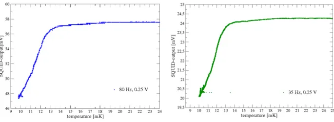
LocalTcmeasurements on this sample were done on two positions within the roughened area marked as I and II in Fig. 4. The planar coil (2.8 mm by 2.8 mm square) was positioned at a distance of 100 µm from the film.
The measurement at location I was carried out with a current of 2.5 µA at 80 Hz and the transition appears at about 11.5 mK. In a further cooldown the coil was placed at position II and the measurement was done
FIGURE 4. Photograph of the sapphire substrate with evap- orated tungsten film. The stripes indicate the electrical con- tacts for a low-current resistiveTc-measurement. The four small squares mark the area of the local measurements done with a planar probe coil.
with a current of 2.5 µA at 35 Hz showing a very similar transition curve at around 12 mK (see Fig. 5). The two localTcmeasurements are in good agreement, hence the properties of the film in the roughened area seem to be approximately homogeneous.
Measurements carried out with the coil positioned over areas of the film that had not been roughened (la- beled as III and IV in Fig. 4) did not show any signal of a superconducting transition in the temperature range down to 8.3 mK. We believe this is due to film stress that appears on the interface between the substrate and the film. As sapphire and tungsten do not have the same lat- tice parameter, tungsten tries to adapt to the crystal struc- ture of the sapphire during evaporation. Under these cir- cumstances the crystal lattice of the tungsten will be dis- torted resulting in tension in the film that can affect the transition temperature [7]. To recheck the result of the localTc-measurement over the roughened area the com- plete film except a small rectangular area in the rough- ened part was removed and a resistiveTc-measurement of the remaining small film was performed showing a sharp transition at 12.3 mK (width of transition of 1.5 mK).
This agrees very well with the local measurements in this area and confirms the validity of the inductive method.
The transition in the resistive low-current measure- ment of the full film starts at about 33 mK and at 9 mK it is not yet complete. Hence there are areas in the film that do not get superconducting down to 9 mK. With the local coil measurements such areas (marked as III and IV in Fig. 4) could be found but no spots with a transition at about 30 mK could be measured. This might be due to the fact that this areas with a higher Tclie on the border of the film or on other, not measured parts.
FIGURE 5. Left: Transition curve measured at position I (see Fig. 4). Right: Transition curve measured at position II. Both measurements were carried out with the planar coil (2.8 mm by 2.8 mm square) at a distance of 100 µm between coil and sample.
4. IMPROVEMENTS
To systematically analyse the local dependence of the transition temperature and to enable mapping theTcdis- tribution over the whole film, a positioning system to move the probe coil at low temperatures is needed. For this we introduced a commercial slip-stick step-scanner from attocube company [8]. The step-scanner is con- venient because it has a large scan range (15 mm) and works at milli Kelvin temperatures. In a first attempt a rough positioning (µm steps) showed that the cryo- stat will warm up during scanning (about 1 K), mostly because of friction of the positioner, but still recovers to base temperature in one to three hours after moving the scanner, depending on the scanning distance. Fur- ther improvements of the size of the probe coil will al- low a higher spatial resolution in the study of the Tc- distribution in our films in the future. In conclusion, our method for contactless local transition temperature mea- surements of thin tungsten films at milli Kelvin temper- ature works and after being upgraded with a positioning system it will provide an opportunity to study system- atically the local dependence ofTc in an area of about 225 mm2in only one cooldown of the cryostat.
REFERENCES
1. G. Angloher et al.,Astroparticle Physics23, 325-339 (2005)
2. G. Angloher et al.,Astroparticle Physics31, 270-276 (2009)
3. W. Meissner and R. Ochsenfeld,Naturwissenschaften21, 787 (1933)
4. Model 581 DC SQUID System,Applied Physics Systems, California, USA, URL: www.appliedphysics.com 5. A. J. Azevede,Rev. Sci. Instrum.54, 1793 (1983)
6. R. J. Soulen and R. B. Dove, SRM: Temperature Reference Standard for Use below 0.5 K, National Bureau of Standards Washington, Special Publication260-62, (1979) 7. R. H. Blumberg and D. P. Seraphim,J. Appl. Phys.33,
163-168 (1962)
8. ANPxy100 piezo positioner,attocubesystems AG, Munich, Germany, URL: www.attocube.com
.