Computer Structure
&
Introduction to Digital Computers
Lecture Notes
by Guy Even
Dept. of Electrical Engineering - Systems, Tel-Aviv University.
Spring 2003
ii
Copyright 2003 by Guy Even Send comments to: guy@eng.tau.ac.il
Printed on June 11, 2003
Contents
1 The digital abstraction 1
1.1 Transistors . . . 1
1.2 From analog signals to digital signals . . . 3
1.3 Transfer functions of gates . . . 5
1.4 The bounded-noise model . . . 6
1.5 The digital abstraction in presence of noise . . . 7
1.5.1 Redefining the digital interpretation of analog signals . . . 7
1.6 Stable signals . . . 9
1.7 Summary . . . 10
2 Foundations of combinational circuits 11 2.1 Boolean functions . . . 11
2.2 Gates as implementations of Boolean functions . . . 11
2.3 Building blocks . . . 12
2.4 Combinational circuits . . . 14
2.5 Cost and propagation delay . . . 18
2.6 Syntax and semantics . . . 19
2.7 Summary . . . 20
3 Trees 21 3.1 Trees of associative Boolean gates . . . 21
3.1.1 Associative Boolean functions . . . 21
3.1.2 or-trees . . . 22
3.1.3 Cost and delay analysis . . . 23
3.2 Optimality of trees . . . 25
3.2.1 Definitions . . . 25
3.2.2 Lower bounds . . . 26
3.3 Summary . . . 29
4 Decoders and Encoders 31 4.1 Notation . . . 31
4.2 Values represented by binary strings . . . 33
4.3 Decoders . . . 34
4.3.1 Brute force design . . . 34
4.3.2 An optimal decoder design . . . 35 iii
iv CONTENTS
4.3.3 Correctness . . . 35
4.3.4 Cost and delay analysis . . . 36
4.4 Encoders . . . 37
4.4.1 Implementation . . . 38
4.4.2 Cost and delay analysis . . . 41
4.4.3 Yet another encoder . . . 42
4.5 Summary . . . 43
5 Combinational modules 47 5.1 Multiplexers . . . 47
5.1.1 Implementation . . . 47
5.2 Cyclic Shifters . . . 49
5.2.1 Implementation . . . 50
5.3 Priority Encoders . . . 53
5.3.1 Implementation of u-penc(n) . . . 54
5.3.2 Implementation of b-penc . . . 55
5.4 Half-Decoders . . . 59
5.4.1 Preliminaries . . . 59
5.4.2 Implementation . . . 60
5.4.3 Correctness . . . 62
5.4.4 Cost and delay analysis . . . 62
5.5 Logical Shifters . . . 63
5.6 Summary . . . 63
6 Addition 65 6.1 Definition of a binary adder . . . 65
6.2 Ripple Carry Adder . . . 66
6.2.1 Correctness proof . . . 66
6.2.2 Delay and cost analysis . . . 67
6.3 Carry bits . . . 67
6.4 Conditional Sum Adder . . . 69
6.4.1 Motivation . . . 69
6.4.2 Implementation . . . 69
6.4.3 Delay and cost analysis . . . 69
6.5 Compound Adder . . . 71
6.5.1 Implementation . . . 72
6.5.2 Correctness . . . 72
6.5.3 Delay and cost analysis . . . 73
6.6 Summary . . . 74
7 Fast Addition 75 7.1 Reduction: sum-bits 7−→ carry-bits . . . 75
7.2 Computing the carry-bits . . . 75
7.2.1 Carry-Lookahead Adders . . . 76
7.2.2 Reduction to prefix computation . . . 79
CONTENTS v
7.3 Parallel prefix computation . . . 81
7.3.1 Implementation . . . 81
7.3.2 Correctness . . . 82
7.3.3 Delay and cost analysis . . . 82
7.4 Putting it all together . . . 83
7.5 Summary . . . 84
8 Signed Addition 85 8.1 Representation of negative integers . . . 85
8.2 Negation in two’s complement representation . . . 86
8.3 Properties of two’s complement representation . . . 88
8.4 Reduction: two’s complement addition to binary addition . . . 89
8.4.1 Detecting overflow . . . 91
8.4.2 Determining the sign of the sum . . . 92
8.5 A two’s-complement adder . . . 93
8.6 A two’s complement adder/subtracter . . . 94
8.7 Additional questions . . . 96
8.8 Summary . . . 98
9 Flip-Flops 99 9.1 The clock . . . 99
9.2 Edge-triggered Flip-Flop . . . 100
9.3 Arbitration . . . 102
9.4 Arbiters - an impossibility result . . . 103
9.5 Necessity of critical segments . . . 105
9.6 An example . . . 106
9.6.1 Non-empty intersection of Ci and Ai . . . 108
9.7 Other types of memory devices . . . 109
9.7.1 D-Latch . . . 109
9.7.2 Clock enabled flip-flips . . . 109
10 Synchronous Circuits 111 10.1 Syntactic definition . . . 111
10.2 Timing analysis: the canonic form . . . 111
10.2.1 Canonic form of a synchronous circuit . . . 113
10.2.2 Timing constraints . . . 113
10.2.3 Sufficient conditions . . . 114
10.2.4 Satisfying the timing constraints . . . 116
10.2.5 Minimum clock period . . . 116
10.2.6 Initialization . . . 117
10.2.7 Functionality . . . 118
10.3 Timing analysis: the general case . . . 119
10.3.1 Timing constraints . . . 119
10.3.2 Algorithm: minimum clock period . . . 120
10.3.3 Algorithm: correctness . . . 121
vi CONTENTS
10.3.4 Algorithm: feasibility of timing constraints . . . 124
10.4 Functionality . . . 124
10.4.1 The zero delay model . . . 125
10.4.2 Simulation . . . 125
10.5 Summary . . . 125
Chapter 1
The digital abstraction
The term a digital circuit refers to a device that works in a binary world. In the binary world, the only values are zeros and ones. Hence, the inputs of a digital circuit are zeros and ones, and the outputs of a digital circuit are zeros and ones. Digital circuits are usually implemented by electronic devices and operate in the real world. In the real world, there are no zeros and ones; instead, what matters is the voltages of inputs and outputs. Since voltages refer to energy, they are continuous1. So we have a gap between the continuous real world and the two-valued binary world. One should not regard this gap as an absurd.
Digital circuits are only an abstraction of electronic devices. In this chapter we explain this abstraction, called the digital abstraction.
In the digital abstraction one interprets voltage values as binary values. The advantages of the digital model cannot be overstated; this model enables one to focus on the digital behavior of a circuit, to ignore analog and transient phenomena, and to easily build larger more complex circuits out of small circuits. The digital model together with a simple set of rules, called design rules, enable logic designers to design complex digital circuits consisting of millions of gates.
1.1 Transistors
Electronic circuits that are used to build computers are mostly build of transistors. Small circuits, called gates are built from transistors. The most common technology used in VLSI chips today is called CMOS, and in this technology there are only two types of transistors:
N-type and P-type. Each transistor has three connections to the outer world, called thegate, source, and drain. Figure 1.1 depicts diagrams describing these transistors.
Although inaccurate, we will refer, for the sake of simplicity, to the gate and source as inputs and to the drain as an output. An overly simple explanation of an N-type transistor in CMOS technology is as follows: If the voltage of the gate is high (i.e. above some threshold v1), then there is little resistance between the source and the drain. Such a small resistance causes the voltage of the drain to equal the voltage of the source. If the voltage of the gate is low (i.e. below some threshold v0 < v1), then there is a very high resistance between the
1unless Quantum Physics is used.
1
2 CHAPTER 1. THE DIGITAL ABSTRACTION
gate gate
N−transistor drain
drain source
P−transistor source
Figure 1.1: Schematic symbols of an N-transistor and P-transistor
source and the drain. Such a high resistance means that the voltage of the drain is unchanged by the transistor (it could be changed by another transistor if the drains of the two transistors are connected). A P-type transistor is behaves in a dual manner: the resistance between drain and the source is low if the gate voltage is belowv0. If the voltage of the gate is above v1, then the source-to-drain resistance is very high.
Note that this description of transistor behavior implies immediately that transistors are highly non-linear. (Recall that a linear function f(x) satisfies f(a·x) = a·f(x).) In transistors, changes of 10% in input values above the threshold v1 have a small effect on the output while changes of 10% in input values between v0 and v1 have a large effect on the output. In particular, this means that transistors do not follow Ohm’s Law (i.e. V =I·R).
Example 1.1 (A CMOS inverter) Figure 1.2 depicts a CMOS inverter. If the input voltage is above v1, then the source-to-drain resistance in the P-transistor is very high and the source-to-drain resistance in the N-transistor is very low. Since the source of the N- transistor is connected to low voltage (i.e. ground), the output of the inverter is low.
If the input voltage is below v0, then the source-to-drain resistance in the N-transistor is very high and the source-to-drain resistance in the P-transistor is very low. Since the source of the P-transistor is connected to high voltage, the output of the inverter is high.
We conclude that the voltage of the output is low when the input is high, and vice-versa, and the device is indeed an inverter.
OUT IN
0 volts 5 volts
N−transistor P−transistor
Figure 1.2: A CMOS inverter
The qualitative description in Example 1.1 hopefully conveys some intuition about how gates are built from transistors. A quantitative analysis of such an inverter requires precise modeling of the functionality of the transistors in order to derive the input-output volt- age relation. One usually performs such an analysis by computer programs (e.g. SPICE).
Quantitative analysis is relatively complex and inadequate for designing large systems like computers. (This would be like having to deal with the chemistry of ink when using a pen.)
1.2. FROM ANALOG SIGNALS TO DIGITAL SIGNALS 3
1.2 From analog signals to digital signals
Ananalog signal is a real functionf : → that describes the voltage of a given point in a circuit as a function of the time. We ignore the resistance and capacities of wires. Moreover, we assume that signals propagate through wires immediately2. Under these assumptions, it follows that the voltage along a wire is identical at all times. Since a signal describes the voltage (i.e. derivative of energy as a function of electric charge), we also assume that a signal is a continuous function.
A digital signal is a function g : → {0,1,non-logical}. The value of a digital signal describes thelogical value carried along a wire as a function of time. To be precise there are two logical values: zero and one. The non-logical value simply means that that the signal is neither zero or one.
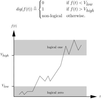
How does one interpret an analog signal as a digital signal? The simplest interpretation is to set a threshold V0. Given an analog signal f(t), the digital signal dig(f(t)) can be defined as follows.
dig(f(t))=4
(0 if f(t)< V0
1 if f(t)> V0 (1.1)
According to this definition, a digital interpretation of an analog signal is always 0 or 1, and the digital interpretation is never non-logical.
There are several problems with the definition in Equation 1.1. One problem with this definition is that all the components should comply with exactly the same threshold V0. In reality, devices are not completely identical; the actual thresholds of different devices vary according to a tolerance specified by the manufacturer. This means that instead of a fixed threshold, we should consider a range of thresholds.
Another problem with the definition in Equation 1.1 is caused by perturbations off(t) around the threshold t. Such perturbations can be caused by noise or oscillations of f(t) before it stabilizes. We will elaborate more on noise later, and now explain why oscillations can occur. Consider a spring connected to the ceiling with a weight w hanging from it. We expect the spring to reach a length ` that is proportional to the weight w. Assume that all we wish to know is whether the length ` is greater than a threshold `t. Sounds simple! But what if ` is rather close to `t? In practice, the length only tends to the length ` as time progresses; the actual length of the spring oscillates around `with a diminishing amplitude.
Hence, the length of the spring fluctuates below and above `t many times before we can decide. This effect may force us to wait for a long time before we can decide if ` < `t. If we return to the definition of dig(f(t)), it may well happen that f(t) oscillates around the threshold V0. This renders the digital interpretation used in Eq. 1.1 useless.
Returning to the example of weighing weights, assume that we have two types of objects:
light and heavy. The weight of a light (resp., heavy) object is at most (resp., at least) w0
(resp., w1). The bigger the gap w1−w0, the easier it becomes to determine if an object is light or heavy (especially in the presence of noise or oscillations).
Now we have two reasons to introduce two threshold values instead of one, namely, different threshold values for different devices and the desire to have a gap between values
2This is a reasonable assumption if wires are short.
4 CHAPTER 1. THE DIGITAL ABSTRACTION interpreted as logical zero and logical one. We denote these thresholds by Vlow and Vhigh, and require thatVlow < Vhigh. An interpretation of an analog signal is depicted in Figure 1.3.
Consider an analog signal f(t). The digital signal dig(f(t)) is defined as follows.
dig(f(t))=4
0 if f(t)< Vlow 1 if f(t)> Vhigh non-logical otherwise.
(1.2)
Vhigh
logical zero f(t)
Vlow
logical one
t
Figure 1.3: A digital interpretation of an analog signal in the zero-noise model.
We often refer to the logical value of an analog signal f. This is simply a shorthand way of referring to the value of the digital signal dig(f).
It is important to note that fluctuations of f(t) are still possible around the threshold values. However, if the two thresholds are sufficiently far away from each other, fluctuations of f do not cause fluctuations of dig(f(t)) between 0 and 1. Instead, we will have at worst fluctuations of dig(f(t)) between a non-logical value and a logical value (i.e. 0 or 1). A fluctuation between a logical value and a non-logical value is much more favorable than a fluctuation between 0 and 1. The reason is that a non-logical value is an indication that the circuit is still in a transient state and a “decision” has not been reached yet.
Assume that we design an inverter so that its output tends to a voltage that is bounded away from the thresholds Vlow and Vhigh. Let us return to the example of the spring with weightwhanging from it. Additional fluctuations in the length of the spring might be caused by wind. This means that we need to consider additional effects so that our model will be useful. In the case of the digital abstraction, we need to take noise into account. Before we consider the effect of noise, we formulate the static functionality of a gate, namely, the values of its output as a function of its stable inputs.
Question 1.1 Try to define an inverter in terms of the voltage of the output as a function of the voltage of the input.
1.3. TRANSFER FUNCTIONS OF GATES 5
1.3 Transfer functions of gates
The voltage at an output of a gate depends on the voltages of the inputs of the gate. This dependence is called the transfer function (or the voltage-transfer characteristic - VTC).
Consider, for example an inverter with an input x and an output y. To make things com- plicated, the value of the signal y(t) at time t is not only a function of the signal x at time t since y(t) depends on the history. Namely, y(t0) is a function of x(t) over the interval (−∞, t0].
Transfer functions are solved by modeling gates with partial differential equations, a rather complicated task. A good approximation of transfer functions is obtain by solving differential equations, still a complicated task that can be computed quickly only for a few transistors. So how are chips that contain millions of chips designed?
The way this very intricate problem is handled is by restricting designs. In particular, only a small set of building blocks is used. The building blocks are analyzed intensively, their properties are summarized, and designers rely on these properties for their designs.
One of the most important steps in characterizing the behavior of a gate is computing its static transfer function. Returning to the example of the inverter, a “proper” inverter has a unique output value point for each input value. Namely, if the input x(t) is stable for a sufficiently long period of time and equals x0, then the outputy(t) stabilizes on a valuey0
that is a function of x0.3 We formalize the definition of a static transfer function of a gate G with one input x and one output y in the following definition.
Definition 1.1 Consider a device G with one input x and one output y. The device G is a gate if its functionality is specified by a function f : → as follows: there exists a∆>0, such that, for every x0 and every t0, ifx(t) =x0 for every t∈[t0−∆, t0], theny(t0) = f(x0).
Such a function f(x) is called the static transfer function of G.
At this point we should point the following remarks:
1. Since circuits operate over a bounded range of voltages, static transfer functions are usually only defined over bounded domains and ranges (say [0,5] volts).
2. To make the definition useful, one should allow perturbations ofx(t) during the interval [t0−∆, t0]. Static transfer functions model physical devices, and hence, are continuous.
This implies the following definition: For every >0, there exist aδ >0 and a ∆ >0, such that
∀t ∈[t1, t2] : |x(t)−x0| ≤δ ⇒ ∀t∈[t1+ ∆, t2] : |y(t)−f(x0)| ≤.
3If this were not the case, then we need to distinguish between two cases: (a) Stability is not reached: this case occurs, for example, with devices called oscillators. Note that such devices must consume energy even when the input is stable. We point out that in CMOS technology it is easy to design circuits that do not consume energy if the input is logical, so such oscillations are avoided. (b) Stability is reached: in this case, if there is more than one stable output value, it means that the device has more than one equilibrium point.
Such a device can be used to store information about the “history”. It is important to note that devices with multiple equilibriums are very useful as storage devices (i.e. they can “remember” a small amount of information). Nevertheless, devices with multiple equilibriums are not “good” candidates for gates, and it is easy to avoid such devices in CMOS technology..
6 CHAPTER 1. THE DIGITAL ABSTRACTION 3. Note that in the above definition ∆ does not depend on x0 (although it may depend on). Typically, we are interested on the values of ∆ only for logical values ofx(t) (i.e.
x(t) ≤Vlow and x(t)≥ Vhigh). Once the value of is fixed, this constant ∆ is called the propagation delayof the gate G and is one of the most important characteristic of a gate.
Question 1.2 Extend Definition 1.1 to gates withn inputs and m outputs.
Finally, we can now define an inverter in the zero-noise model. Observe that according to this definition a device is an inverter if its static transfer function satisfies a certain property.
Definition 1.2 (inverter in zero-noise model) A gate G with a single input x and a single output y is an inverter if its static transfer function f(z) satisfies the following the following two conditions:
1. If z < Vlow, then f(z)> Vhigh. 2. If z > Vhigh, then f(z)< Vlow.
The implication of this definition is that if the logical value of the input xis zero (resp., one) during an interval [t1, t2] of length at least ∆, then the logical value of the output y is one (resp., zero) during the interval [t1 + ∆, t2].
How should we define other gates such anand-gates,xor-gates, etc.? As in the definition of an inverter, the definition of anand-gate is simply a property of its static transfer function.
Question 1.3 Define a nand-gate.
We are now ready to strengthen the digital abstraction so that it will be useful also in the presence of bounded noise.
1.4 The bounded-noise model
Consider a wire from point A to point B. Let A(t) (resp., B(t)) denote the analog signal measured at pointA(resp.,B). We would like to assume that wires have zero resistance, zero capacitance, and that signals propagate through a wire with zero delay. This assumption means that the signalsA(t) andB(t) should be equal at all times. Unfortunately, this is not the case; the main reason for this discrepancy is noise.
There are many sources of noise. The main source is heat that causes electrons to move randomly. These random movements do not cancel out perfectly, and random currents are created. These random currents create perturbations in the voltage of a wire. The difference between the signals B(t) and A(t) is a noise signal.
Consider, for example, the setting of additive noise: A is an output of an inverter and B is an input of another inverter. We consider the signal A(t) to be a reference signal. The signal B(t) is the sum A(t) +nB(t), where nB(t) is the noise signal.
1.5. THE DIGITAL ABSTRACTION IN PRESENCE OF NOISE 7 The bounded-noise model assumes that the noise signal along every wire has a bounded absolute value. We will use a slightly simplified model in which there is a constant > 0 such that the absolute value of all noise signals is bounded by . We refer to this model as the uniform bounded noise model. The justification for assuming that noise is bounded is probabilistic. Noise is a random variable whose distribution has a rapidly diminishing tail.
This means that if the bound is sufficiently large, then the probability of the noise exceeding this bound during the lifetime of a circuit is negligibly small.
1.5 The digital abstraction in presence of noise
Consider two inverters, where the output of one gate feeds the input of the second gate.
Figure 1.4 depicts such a circuit that consists of two inverters.
Assume that the input x has a value that satisfies: (a) x > Vhigh, so the logical value of x is one, and (b) y=Vlow−0, for a very small 0 >0. This might not be possible with every inverter, but Definition 1.2 does not rule out such an inverter. (Consider a transfer function with f(Vhigh) =Vlow, and xslightly higher than Vhigh.) Since the logical value of y is zero, it follows that the second inverter, if not faulty, should output a value z that is greater than Vhigh. In other words, we expect the logical value of z to be 1. At this point we consider the effect of adding noise.
Let us denote the noise added to the wire y by ny. This means that the input of the second inverter equals y(t) +ny(t). Now, if ny(t) > 0, then the second inverter is fed a non-logical value! This means that we can no longer deduce that the logical value of z is one. We conclude that we must use a more resilient model; in particular, the functionality of circuits should not be affected by noise. Of course, we can only hope to be able to cope with bounded noise, namely noise whose absolute value does not exceed a certain value .
y z x
Figure 1.4: Two inverters connected in series.
1.5.1 Redefining the digital interpretation of analog signals
The way we deal with noise is that we interpret input signals and output signals differently.
An input signal is a signal measured at an input of a gate. Similarly, an output signal is a signal measured at an output of a gate. Instead of two thresholds, Vlow andVhigh, we define the following four thresholds:
• Vlow,in - an upper bound on a voltage of an input signal interpreted as a logical zero.
• Vlow,out - an upper bound on a voltage of an output signal interpreted as a logical zero.
8 CHAPTER 1. THE DIGITAL ABSTRACTION
• Vhigh,in - a lower bound on a voltage of an input signal interpreted as a logical one.
• Vhigh,out - a lower bound on a voltage of an output signal interpreted as a logical one.
These four thresholds satisfy the following equation:
Vlow,out< Vlow,in < Vhigh,in< Vhigh,out. (1.3) Figure 1.5 depicts these four thresholds. Note that the interpretation of input signals is less strict than the interpretation of output signals. The actual values of these four thresholds depend on the transfer functions of the devices we wish to use.
The differences Vlow,in−Vlow,out and Vhigh,out −Vhigh,in are called noise margins.
Our goal is to show that noise whose absolute value is less than the noise margin will not change the logical value of an output signal. Indeed, if the absolute value of the noise n(t) is bounded by the noise margins, then an output signal fout(t) that is below Vlow,out will result with an input signal fin(t) =fout(t) +n(t) that does not exceed Vlow,in.
Vhigh,out
Vlow,out
logical zero - output Vhigh,in
Vlow,in
logical zero - input logical one - output
logical one - input
t f(t)
Figure 1.5: A digital interpretation of an input and output signals.
Consider an input signal fin(t). The digital signal dig(fin(t)) is defined as follows.
dig(fin(t))=4
0 if fin(t)< Vlow,in 1 if fin(t)> Vhigh,in non-logical otherwise.
(1.4)
Consider an output signal fout(t). The digital signal dig(fout(t)) is defined analogously.
dig(fout(t))=4
0 if fout(t)< Vlow,out 1 if fout(t)> Vhigh,out non-logical otherwise.
(1.5)
1.6. STABLE SIGNALS 9 Observe that sufficiently large noise margins imply that noise will not change the logical values of signals.
We can now fix the definition of an inverter so that bounded noise added to outputs, does not affect logical interpretation of signals.
Definition 1.3 (inverter in the bounded-noise model) A gate Gwith a single input x and a single output y is an inverter if its static transfer function f(z) satisfies the following the following two conditions:
1. If z < Vlow,in, then f(z)> Vhigh,out. 2. If z > Vhigh,in, then f(z)< Vlow,out.
Question 1.4 Define a nand-gate in the bounded-noise model.
Question 1.5 Consider the function f(x) = 1−x over the interval [0,1]. Suppose that f(x) is a the transfer function of a device C. Can you define threshold values Vlow,out <
Vlow,in < Vhigh,in < Vhigh,out so that C is an inverter according to Definition 1.3?
Question 1.6 Consider a function f : [0,1] → [0,1]. Suppose that: (i) f(0) = 1, and f(1) = 0, (ii) f(x) is monotone decreasing, (iii) the derivative f0(x) of f(x) satisfies the following conditions: f0(x)is continuous and there is an interval(α, β)such that f0(x)<−1 for every x∈(α, β). And, (iv) there exists a point x0 ∈(α, β) such that f(x0) =x0.
Prove that one can define threshold values Vlow,out < Vlow,in < Vhigh,in < Vhigh,out so that C is an inverter according to Definition 1.3?
Hint: consider a δ > 0 and set Vlow,in = x0 −δ and Vhigh,in = x0 +δ. What is the largest value of δ one can use?
Question 1.7 Try to characterize transfer functionsg(x)that correspond to inverters. Namely, if Cg is a device, the transfer function of which equals g(x), then one can define threshold values that satisfy Definition 1.3.
1.6 Stable signals
In this section we define terminology that will be used later. To simplify notation we define these terms in the zero-noise model. We leave it to the curious reader to extend the definitions and notation below to the bounded-noise model.
An analog signal f(t) is said to be logical at time t if dig(f(t)) ∈ {0,1}. An analog signal f(t) is said to be stableduring the interval [t1, t2] iff(t) is logical for everyt ∈[t1, t2].
Continuity of f(t) and the fact thatVlow < Vhigh imply the following claim.
Claim 1.1 If an analog signal f(t) is stable during the interval [t1, t2] then one of the fol- lowing holds:
1. dig(f(t)) = 0, for every t∈[t1, t2], or
10 CHAPTER 1. THE DIGITAL ABSTRACTION 2. dig(f(t)) = 1, for every t∈[t1, t2].
From this point we will deal with digital signals and use the same terminology. Namely, a digital signal x(t) is logical at time t if x(t) ∈ {0,1}. A digital signal is stable during an interval [t1, t2] if x(t) is logical for every t ∈[t1, t2].
1.7 Summary
In this chapter we presented the digital abstraction of analog devices. For this purpose we defined analog signals and their digital counterpart, called digital signals. In the digital abstraction, analog signals are interpreted either as zero, one, or non-logical.
We discussed noise and showed that to make the model useful, one should set stricter requirements from output signals than from input signals. Our discussion is based on the bounded-noise model in which there is an upper bound on the absolute value of noise.
We defined gates using transfer functions and static transfer functions. This functions describe the analog behavior of devices. We also defined the propagation delay of a device as the amount of time that input signals must be stable to guarantee stability of the output of a gate.
Chapter 2
Foundations of combinational circuits
In this chapter we define and study combinational circuits. Our goal is to prove two theorems:
(A) Every Boolean function can be implemented by a combinational circuit, and (B) Every combinational circuit implements a Boolean function.
2.1 Boolean functions
Let {0,1}n denote the set of n-bit strings. A Boolean function is defined as follows.
Definition 2.1 A function f :{0,1}n → {0,1}k is called a Boolean function.
2.2 Gates as implementations of Boolean functions
A gate is a device that has inputs and outputs. The inputs and outputs of a gate are often referred to as terminals, ports, or even pins. In combinational gates, the relation between the logical values of the outputs and the logical values of the inputs is specified by a Boolean function. It takes some time till the logical values of the outputs of a gate properly reflect the value of the Boolean function. We say that a gate is consistentif this relation holds. To simplify notation, we consider a gateGwith 2 inputs, denoted byx1, x2, and a single output, denoted by y. We denote the digital signal at terminal x1 by x1(t). The same notation is used for the other terminals. Consistency is defined formally as follows:
Definition 2.2 A gate G is consistent with a Boolean function f at time t if the input values are digital at time t and
y(t) =f(x1(t), x2(t)).
The propagation delay is the amount of time that elapses till a gate becomes consistent. The following definition defines when a gate implements a Boolean function with propagation delay tpd.
Definition 2.3 A gate G implements a Boolean functionf :{0,1}2→ {0,1} with propaga- tion delay tpd if the following holds.
11
12 CHAPTER 2. FOUNDATIONS OF COMBINATIONAL CIRCUITS For every σ1, σ2 ∈ {0,1}, if xi(t) =σi, for i= 1,2, during the interval [t1, t2], then
∀t ∈[t1+tpd, t2] : y(t) =f(σ1, σ2).
The following remarks should be well understood before we continue:
1. The above definition can be stated in a more compact form. Namely, a gateG imple- ments a Boolean function f : {0,1}n → {0,1} with propagation delay tpd if stability of the inputs of Gin the interval [t1, t2] implies that the gate Gis consistent withf in the interval [t1+tpd, t2].
2. Ift2 < t1+tpd, then the statement in the above definition is empty. It follows that the inputs of a gate must be stable for at least a period of tpd, otherwise, the gate need not reach consistency.
3. Assume that the gate G is consistent at time t2, and that at least one input is not stable in the interval (t2, t3). We do not assume that the output of G remains stable after t2. The contamination delay of a gate is the amount of time that the output of a consistent gate remains stable after its inputs stop being stable. Throughout this course, unless stated otherwise, we will make the most “pessimistic” assumption about the contamination delay. Namely, we will assume that the contamination delay is zero.
4. If a gateGimplements a Boolean functionf :{0,1}n→ {0,1}with propagation delay tpd, then G also implements a Boolean function f :{0,1}n → {0,1}with propagation delay t0, for every t0 ≥tpd. It follows that it is legitimate to use upper bounds on the actual propagation delay. Pessimistic assumptions should not render a circuit incorrect.
In fact, the actual exact propagation delay is very hard to compute. It depends on x(t) (i.e how fast does the input change?). This is why we resort to upper bounds on the propagation delays.
2.3 Building blocks
The building blocks of combinational circuits are gates and wires. In fact, we will need to consider nets which are generalizations of wires.
Gates. A gate, as seen in Definition 2.3 is a device that implements a Boolean function.
The fan-in of a gate Gis the number of inputs terminals ofG(i.e. the number of bits in the domain of the Boolean function that specifies the functionality of G). The basic gates that we will be using as building blocks for combinational circuits have a constant fan-in (i.e. at most 2−3 input ports). The basic gates that we consider are: inverter (not-gate),or-gate, nor-gate, and-gate, nand-gate, xor-gate, nxor-gate, multiplexer (mux).
The input ports of a gate G are denoted by the set {in(G)i}ni=1, where n denotes the fan-in of G. The output ports of a gate G are denoted by the set {out(G)i}ki=1, where k denotes the number of output ports of G.
2.3. BUILDING BLOCKS 13 Wires and nets. A wire is a connection between two terminals (e.g. an output of one gate and an input of another gate). In the zero-noise model, the signals at both ends of a wire are identical.
Very often we need to connect several terminals (i.e. inputs and outputs of gates) to- gether. We could, of course, use any set of edges (i.e. wires) that connects these terminals together. Instead of specifying how the terminals are physically connected together, we use nets.
Definition 2.4 A net is a subset of terminals that are connected by wires.
In the digital abstraction we assume that the signals all over a net are identical (why?). The fan-out of a net N is the number of input terminals that are connected by N.
The issue of drawing nets is a bit confusing. Figure 2.1 depicts three different drawings of the same net. All three nets contain an output terminal of an inverter and 4 input terminals of inverters. However, the nets are drawn differently. Recall that the definition of a net is simply a subset of terminals. We may draw a net in any way that we find convenient or aesthetic. The interpretation of the drawing is that terminals that are connected by lines or curves constitute a net.
Figure 2.1: Three equivalent nets.
Consider a net N. We would like to define the digital signalN(t) for the whole net. The problem is that due to noise (and other reasons) the analog signals at different terminals of the net might not equal each other. This might cause the digital interpretations of analog signals at different terminals of the net to be different, too. We solve this problem by defining N(t) to logical only if there is a consensus among all the digital interpretations of analog signals at different terminals of the net. Namely, N(t) is zero (one) if the digital values of all the analog signals along the net are zero (one). If there is no consensus, then N(t) is non- logical. Recall that, in the bounded-noise model, different thresholds are used to interpret the digital values of the analog signals measured in input and output terminals.
We say that a netN feeds an input terminal tif the input terminaltis inN. We say that a net N is fed by an output terminal t if t is in N. Figure 2.2 depicts an output terminal that feeds a net and an input terminal that is fed by a net. The notion of feeding and being fed implies a direction according to which information “flows”; namely, information is
“supplied” by output terminals and is “consumed” by input terminals. From an electronic point of view, in “pure” CMOS gates, output terminals are connected via resistors either to the ground or to the power. Input terminals are connected only to capacitors.
The following definition captures the type of nets we would like to use. We call these nets simple.
14 CHAPTER 2. FOUNDATIONS OF COMBINATIONAL CIRCUITS
a net fed by terminal t’
t t’
a net that feeds terminal t
Figure 2.2: A terminal that is fed by a net and a terminal that feeds a net.
Definition 2.5 A net N is simple if (a) N is fed by exactly one output terminal, and (b) N feeds at least one input terminal.
A simple net N that is fed by the output terminal t and feeds the input terminals {ti}i∈I, can be modeled by wires {wi}i∈I. Each wire wi connects t and ti. In fact, since information flows in one direction, we may regard each wire wi as a directed edge t →ti.
It follows that a circuit, all the nets of which are simple, may be modeled by a directed graph. We define this graph in the following definition.
Definition 2.6 Let C denote a circuit, all the nets of which are simple. The directed graph DG(C) is defined as follows. The vertices of the graph DG(C) are the gates of C. The directed edges correspond to the wires as follows. Consider a simple net N fed by an output terminal t that feeds the input terminals {ti}i∈I. The directed edges that correspond to N are u → vi, where u is the gate that contains the output terminal t and vi is the gate that contains the input terminal ti.
Note that the information of which terminal is connected to each wire is not maintained in the graph DG(C). One could of course label each endpoint of an edge in DG(C) with the name of the terminal the edge is connected to.
2.4 Combinational circuits
Question 2.1 Consider the circuits depicted in Figure 2.3. Can you explain why these are not valid combinational circuits?
Before we define combinational circuits it is helpful to define two types of special gates:
an input gate and an output gate. The purpose of these gates is to avoid endpoints in nets that seem to be not connected (for example, all the nets in the circuit on the right in Figure 2.3 have endpoints that are not connected to a gate).
Definition 2.7 (input and output gates) An input gate is a gate with zero inputs and a single output. An output gate is a gate with one input and zero outputs.
Figure 2.4 depicts an input gate and an output gate. Inputs from the “external world” are fed to a circuit via input gates. Similarly, outputs to the “external world” are fed by the circuit via output gates.
2.4. COMBINATIONAL CIRCUITS 15
Figure 2.3: Two examples of non-combinational circuits.
Output Gate Input Gate
Figure 2.4: An input gate and an output gate
Consider a fixed set of gate-types (e.g. inverter, nand-gate, etc.); we often refer to such a set of gate-types as alibrary. We associate with every gate-type in the library the number of inputs, the number of outputs, and the Boolean function that specifies its functionality.
Let G denote the set of gates in a circuit. Every gate G ∈ G is an instance of a gate from the library. Formally, the gate-type of a gate G indicates the library element that corresponds to G (e.g. “the gate-type of G is an inverter”). To simplify the discussion, we simply refer to a gate G as an inverter instead of saying that its gate-type is an inverter.
We now present a syntactic definition of combinational circuits.
Definition 2.8 (syntactic definition of combinational circuits) A combinational cir- cuit is a pair C =hG,N i that satisfies the following conditions:
1. G is a set of gates.
2. N is a set of nets over terminals of gates in G.
3. Every terminal t of a gate G∈ G belongs to exactly one net N ∈ N. 4. Every net N ∈ N is simple.
5. The directed graph DG(C)is acyclic.
Note that Definition 2.8 is independent of the gate types. One need not even know the gate- type of each gate to determine whether a circuit is combinational. Moreover, the question of whether a circuit is combinational is a purely topological question (i.e. are the intercon- nections between gates legal?).
16 CHAPTER 2. FOUNDATIONS OF COMBINATIONAL CIRCUITS Question 2.2 Which conditions in the syntactic definition of combinational circuits are violated by the circuits depicted in Figure 2.3?
We list below a few properties that explain why the syntactic definition of combinational circuits is so important. In particular, these properties show that the syntactic definition of combinational circuits implies well defined semantics.
1. Completeness: for every Boolean functionf, there exists a combinational circuit that implements f. We leave the proof of this property as an exercise for the reader.
2. Soundness: every combinational circuit implements a Boolean function. Note that it is NP-Complete to decide if the Boolean function that is implemented by a given combinational circuit with one output ever gets the value 1.
3. Simulation: given the digital values of the inputs of a combinational circuit, one can simulate the circuit in linear time. Namely, one can compute the digital values of the outputs of the circuit that are output by the circuit once the circuit becomes consistent.
4. Delay analysis: given the propagation delays of all the gates in a combinational circuit, one can compute in linear time an upper bound on the propagation delay of the circuit.
Moreover, computing tighter upper bounds is again NP-Complete.
The last three properties are proved in the following theorem by showing that in a combinational circuit every net implements a Boolean function of the inputs of the circuit.
Theorem 2.1 (Simulation theorem of combinational circuits) Let C = hG,N i de- note a combinational circuit that contains k input gates. Let {xi}ki=1 denote the output ter- minals of the input gates in C. Assume that the digital signals {xi(t)}ki=1 are stable during the interval [t1, t2]. Then, for every net N ∈ N there exist:
1. a Boolean function fN :{0,1}k→ {0,1}, and 2. a propagation delay tpd(N)
such that
N(t) =fN(x1(t), x2(t), . . . , xk(t)), for every t∈[t1+tpd(N), t2].
We can simplify the statement of Theorem 2.1 by considering each net N ∈ N as an output of a combinational circuit withk inputs. The theorem then states that every net implements a Boolean function with an appropriate propagation delay.
We use ~x(t) to denote the vector x1(t), . . . , xk(t).
2.4. COMBINATIONAL CIRCUITS 17 Proof: Let n denote the number of gates in G and m the number of nets in N. The directed graph DG(C) is acyclic. It follows that we can topologically sort the vertices of DG(C). Letv1, v2, . . . , vndenote the set of gatesG according to the topological order. (This means that if there is a directed path from vi to vj in DG(C), then i < j.) We assume, without loss of generality, that v1, . . . , vk is the set of input gates.
LetNi denote the subset of nets inN that are fed by gatevi. Note that if vi is an output gate, then Ni is empty. Let e1, e2, . . . , em denote an ordering of the nets in N such that nets inNi precede nets inNi+1, for every i < n. In other words, we first list the nets fed by gate v1, followed by a list of the nets fed by gate v2, etc.
Having defined a linear order on the gates and on the nets, we are now ready to prove the theorem by induction on m (the number of nets).
Induction hypothesis: For everyi≤m0 there exist:
1. a Boolean function fei :{0,1}k → {0,1}, and 2. a propagation delay tpd(ei)
such that the network ei implements the Boolean functionfei with propagation delaytpd(ei).
Induction Basis: We prove the induction basis for m0 = k. Consider an i ≤ k. Note that, for every i ≤ k, ei is fed by the input gate vi. Let xi denote the output terminal of vi. It follows that the digital signal along ei always equals the digital signalxi(t). Hence we define fei to be simply the projection on the ith component, namely fe1(σ1, . . . , σk) = σi. The propagation delay tpd(ei) is zero. The induction basis follows.
Induction Step: Assume that the induction hypothesis holds for m0 < m. We wish to prove that it also holds form0+ 1. Consider the netem0+1. Let vi denote the gate that feeds the net em0+1. To simplify notation, assume that the gate vi has two terminals that are fed by the nets ej and ek, respectively. The ordering of the nets guarantees that j, k ≤ m0. By the induction hypothesis, the net ej (resp., ek) implements a Boolean function fej (resp., fek) with propagation delay tpd(ej) (resp., tpd(ek)). This implies that both inputs to gate vi
are stable during the interval
[t1+ max{tpd(ej), tpd(ek)}, t2].
Gate vi implements a Boolean function fvi with propagation delay tpd(vi). It follows that the output of gate vi equals
fvi(fej(~x(t)), fek(~x(t))) during the interval
[t1+ max{tpd(ej), tpd(ek)}+tpd(vi), t2].
We definefem0+1 to be the Boolean function obtained by the composition of Boolean functions fem0+1(~σ) =fvi(fej(~σ), fek(~σ)). We define tpd(em0+1) to be max{tpd(ej), tpd(ek)}+tpd(vi), and
the induction step follows. 2
The digital abstraction allows us to assume that the signal corresponding to every net in a combinational circuit is logical (provided that the time that elapses since the inputs
18 CHAPTER 2. FOUNDATIONS OF COMBINATIONAL CIRCUITS become stable is at least the propagation delay). This justifies the convention of identifying a net with the digital value of the net.
The proof of Theorem 2.1 leads to two related algorithms. One algorithm simulates a combinational circuit, namely, given a combinational circuit and a Boolean assignment to the inputs ~x, the algorithm can compute the digital signal of every net after a sufficient amount of time elapses. The second algorithm computes the propagation delay of each net.
Of particular interest are the nets that feed the output gates of the combinational circuit.
Hence, we may regard a combinational circuit as a “macro-gate”. All instances of the same combinational circuit implement the same Boolean function and have the same propagation delay.
The algorithms are very easy. For convenience we describe them as one joint algorithm.
First, the directed graph DG(C) is constructed (this takes linear time). Then the gates are sorted in topological order (this also takes linear time). This order also induced an order on the nets. Now a sequence ofrelaxationsteps take place for nets e1, e2, . . . , em. In a relaxation step the propagation delay of a net ei two computations take place:
1. The Boolean value ofei is set to
fvj(I~vj),
where vj is the gate that feeds the net ei and I~vj is the binary vector that describes the values of the nets that feed gate vj.
2. The propagation delay of the gate that feeds ei is set to
tpd(ei)←tpd(vj) + max{tpd(e0)}{e0 feeds vj}.
If the number of outputs of each gate is constant, then the total amount of time spend in the relaxation steps is linear, and hence the running time of this algorithm is linear. (Note that the input length is the number of gates plus the sum of the sizes of the nets.)
Question 2.3 Prove that the total amount of time spent in the relaxation steps is linear if the fan-in of each gate is constant (say, at most 3).
Note that it is not true that each relaxation step can be done in constant time if the fan-in of the gates is not constant. Can you still prove linear running time if the fan-in of the gates is not constant but the number of outputs of each gate is constant?
Can you suggest a slight weakening of this restriction which still maintains a linear run- ning time?
2.5 Cost and propagation delay
In this section we define the cost and propagation delay of a combinational circuit.
We associate a cost with every gate. We denote the cost of a gate Gby c(G).
Definition 2.9 The cost of a combinational circuit C =hG,N i is defined by c(C)=4 X
G∈G
c(G).
2.6. SYNTAX AND SEMANTICS 19 The following definition defined the propagation delay of a combinational circuit.
Definition 2.10 The propagation delay of a combinational circuit C =hG,N i is defined by tpd(C)= max4
N∈Ntpd(N).
We often refer to the propagation delay of a combinational circuit as its depth or simply its delay.
Definition 2.11 A sequence p = {v0, v1, . . . , vk} of gates from G is a path in a combina- tional circuit C =hG,N i if p is a path in the directed graphDG(C).
The propagation delay of a path p is defined as tpd(p) =X
v∈p
tpd(v).
The proof of the following claim follows directly from the proof of Theorem 2.1.
Claim 2.2 The propagation delay of a combinational circuit C=hG,N i equals tpd(C) = max
paths p
tpd(p)
Paths, the delay of which equals the propagation delay of the circuit, are calledcritical paths.
Question 2.4 1. Describe a combinational circuit with n gates that has at least 2n/2 paths. Can you describe a circuit with 2n different paths?
2. In Claim 2.2 the propagation delay of a combinational circuit is defined to be the maximum delay of a path in the circuit. The number of paths can be exponential in n.
How can we compute the propagation delay of a combinational circuit in linear time?
M¨uller and Paul compiled the following costs and delays of gates. These figures were obtained by considering ASIC libraries of two technologies and normalizing them with respect to the cost and delay of an inverter. They referred to these figures as Motorola and Venus.
Table 2.1 summarizes the normalized costs and delays in these technologies.
2.6 Syntax and semantics
In this chapter we have used both explicitly and implicitly the terms syntax and semantics.
These terms are so fundamental that they deserve a section.
The term semantics (in our context) refers to the function that a circuit implements.
Often, the semantics of a circuit is referred to as the functionality or even the behavior of the circuit. In general, the semantics of a circuit is a formal description that relates the outputs of the circuit to the inputs of the circuit. In the case of combinational circuits,
20 CHAPTER 2. FOUNDATIONS OF COMBINATIONAL CIRCUITS
Gate Motorola Venus
cost delay cost delay
inv 1 1 1 1
and,or 2 2 2 1
nand, nor 2 1 2 1 xor,nxor 4 2 6 2
mux 3 2 3 2
Table 2.1: Costs and delays of gates
semantics are described by Boolean functions. Note that in non-combinational circuits, the output depends not only on the current inputs, so semantics cannot be described simply by a Boolean function.
The term syntax refers to a formal set of rules that govern how “grammatically correct”
circuits are constructed from smaller circuits (just as sentences are built of words). In the syntactic definition of combinational circuits the functionality (or gate-type) of each gate is not important. The only part that matters is that the rules for connecting gates together are followed. Following syntax in itself does not guarantee that the resulting circuit is useful.
Following syntax is, in fact, a restriction that we are willing to accept so that we can enjoy the benefits of well defined functionality, simple simulation, and simple timing analysis. The restriction of following syntax rules is a reasonable choice since every Boolean function can be implemented by a syntactically correct combinational circuit.
2.7 Summary
Combinational circuits were formally defined in this chapter. We started by considering the basic building blocks: gates and wires. Gates are simply implementations of Boolean functions. The digital abstraction enables a simple definition of what it means to implement a Boolean function f. Given a propagation delay tpd and stable inputs whose digital value is~x, the digital values of the outputs of a gate equal f(~x) after tpd time elapses.
Wires are used to connect terminals together. Bunches of wires are used to connect multiple terminals to each other and are called nets. Simple nets are nets in which the direction in which information flows is well defined; from output terminals of gates to input terminals of gates.
The formal definition of combinational circuits turns out to be most useful. It is a syn- tactic definition that only depends on the topology of the circuit, namely, how the terminals of the gates are connected. One can check in linear time whether a given circuit is indeed a combinational circuit. Even though the definition ignores functionality, one can compute in linear time the digital signals of every net in the circuit. Moreover, one can also compute in linear time the propagation delay of every net.
Two quality measures are defined for every combinational circuit: cost and propagation delay. The cost of a combinational circuit is the sum of the costs of the gates in the circuit.
The propagation delay of a combinational is the maximum delay of a path in the circuit.
Chapter 3 Trees
In this chapter we deal with combinational circuits that have a topology of a tree. We begin by considering circuits for associative Boolean function. We then prove two lower bounds;
one for cost and one for delay. These lower bounds do not assume that the circuits are trees.
The lower bounds prove that trees have optimal cost and balanced trees have optimal delay.
3.1 Trees of associative Boolean gates
In this section, we deal with combinational circuits that have a topology of a tree. All the gates in the circuits we consider are instances of the same gate that implements an associative Boolean function.
3.1.1 Associative Boolean functions
Definition 3.1 A Boolean function f :{0,1}2 → {0,1} is associative if f(f(σ1, σ2), σ3) =f(σ1, f(σ2, σ3)),
for every σ1, σ2, σ3 ∈ {0,1}.
Question 3.1 List all the associative Boolean functions f :{0,1}2→ {0,1}.
A Boolean function defined over the domain {0,1}2 is often denoted by a dyadic operator, say . Namely, f(σ1, σ2) is denoted by σ1 σ2. Associativity of a Boolean function is then formulated by
∀σ1, σ2, σ3 ∈ {0,1} : (σ1 σ2)σ3 =σ1(σ2σ3).
This implies that one may omit parenthesis from expressions involving an associative Boolean function and simply write σ1σ2σ3. Thus we obtain a function defined over{0,1}n from a dyadic Boolean function. We formalize this composition of functions as follows.
Definition 3.2 Let f : {0,1}2 → {0,1} denote a Boolean function. The function fn : {0,1}n→ {0,1}, for n≥2 is defined by induction as follows.
21
22 CHAPTER 3. TREES 1. If n = 2 then f2 ≡ f (the sign ≡ is used instead of equality to emphasize equality of
functions).
2. If n > 2, then fn is defined based on fn−1 as follows:
fn(x1, x2, . . . xn)=4 f(fn−1(x1, . . . , xn−1), xn).
Iff(x1, x2) is an associative Boolean function, then one could definefnin many equivalent ways, as summarized in the following claim.
Claim 3.1 If f :{0,1}2 → {0,1} is an associative Boolean function, then fn(x1, x2, . . . xn) =f(fk(x1, . . . , xk), fn−k(xk+1, . . . , xn)), for every k∈[2, n−2].
Question 3.2 Show that the set of functions fn(x1, . . . , xn) that are induced by associative Boolean functions f :{0,1}2→ {0,1} is
{constant 0,constant 1, x1, xn,and,or,xor,nxor}.
The implication of Question 3.2 is that there are only four non-trivial functions fn (which?).
In the rest of this section we will only consider the Boolean function or. The discussion for the other three non-trivial functions is analogous.
3.1.2 or -trees
Definition 3.3 A combinational circuit C = hG,N i that satisfies the following conditions is called an or-tree(n).
1. Input: x[n−1 : 0].
2. Output: y∈ {0,1}
3. Functionality: y=or(x[0], x[1],· · ·, x[n−1]).
4. Gates: All the gates in G are or-gates.
5. Topology: The underlying graph ofDG(C)(i.e. undirected graph obtained by ignoring edge directions) is a rooted binary tree.
Consider the binary tree T corresponding to the underlying graph of DG(C), where C is an or-tree(n). The root of T corresponds to the output gate of C. The leaves of T correspond to the input gates of C, and the interior nodes in T correspond to or-gates in C.
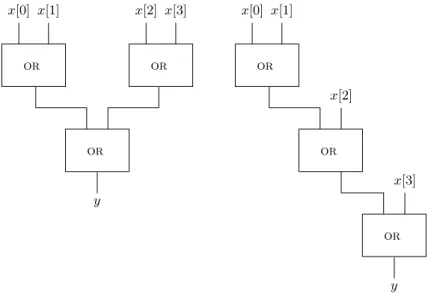
Claim 3.1 provides a “recipe” for implementing an or-tree using or-gates. Consider a rooted binary tree with n leaves. The inputs are fed via the leaves, anor-gate is positioned in every node of the tree, and the output is obtained at the root. Figure 3.1 depicts two or-tree(n) forn = 4.
One could also define an or-tree(n) recursively, as follows.
3.1. TREES OF ASSOCIATIVE BOOLEAN GATES 23
or
or x[3]
y x[2]
or
or or
x[0] x[1] x[2] x[3]
or x[0] x[1]
y
Figure 3.1: Two implementations of anor-tree(n) withn = 4 inputs.
Definition 3.4 An or-tree(n) is defined recursively as follows (see Figure 3.2):
1. Basis: a single or-gate is an or-tree(2).
2. Step: an or(n)-tree is a circuit in which
(a) the output is computed by an or-gate, and
(b) the inputs of this or-gate are the outputs of or-tree(n1) & or-tree(n2), where n=n1+n2.
Question 3.3 Design a zero-tester defined as follows.
Input: x[n−1 : 0].
Output: y Functionality:
y= 1 iff x[n−1 : 0] = 0n. 1. Suggest a design based on an or-tree.
2. Suggest a design based on an and-tree.
3. What do you think about a design based on a tree of nor-gates?
3.1.3 Cost and delay analysis
You may have noticed that both or-trees depicted in Figure 3.1 contain three or-gates.
However, their delay is different. The following claim summarizes the fact that all or-trees have the same cost.
Claim 3.2 The cost of every or-tree(n) is (n−1)·c(or).
24 CHAPTER 3. TREES
or
or or-tree(n
1) or-tree(n
2)
Figure 3.2: A recursive definition of an or-tree(n).
Proof: The proof is by induction on n. The induction basis, for n = 2, follows because or-tree(2) contains a single or-gate. We now prove the induction step.
Let C denote an or-tree(n), and let g denote the or-gate that outputs the output of C. The gate g is fed by two wires e1 and e2. The recursive definition of or-gate(n) implies the following. For i = 1,2, the wire ei is the output of Ci, where Ci is an or-tree(ni).
Moreover, n1 +n2 = n. The induction hypothesis states that c(C1) = (n1 −1)·c(or) and c(C2) = (n2−1)·c(or). We conclude that
c(C) =c(g) +c(C1) +c(C2)
= (1 +n1−1 +n2−1)·c(or)
= (n−1)·c(or),
and the claim follows. 2
The following question shows that the delay of anor-tree(n) can be dlog2ne ·tpd(or), if a balanced tree is used.
Question 3.4 This question deals with different ways to construct balanced trees. The goal is to achieve a depth of dlog2ne.
1. Prove that if Tn is a rooted binary tree with n leaves, then the depth of Tn is at least dlog2ne.
2. Assume that n is a power of 2. Prove that the depth of a complete binary tree with n leaves is log2n.
3.2. OPTIMALITY OF TREES 25 3. Prove that for every n > 2 there exists a pair of positive integers a, b such that (1)
a+b=n, and (2) max{dlog2ae,dlog2be} ≤ dlog2ne −1.
4. Consider the following recursive algorithm for constructing a binary tree with n ≥ 2 leaves.
(a) The case that n≤2 is trivial (two leaves connected to a root).
(b) Ifn > 2, then let a, b be any pair of positive integers such that (i) n =a+b and (ii) max{dlog2ae,dlog2be} ≤ dlog2ne − 1. (Such a pair exists by the previous item.)
(c) Compute trees Ta and Tb. Connect their roots to a new root to obtainTn. Prove that the depth of Tn is at most dlog2ne.
3.2 Optimality of trees
In this section we deal with the following questions: What is the best choice of a topology for a combinational circuit that implements the Boolean function orn? Is a tree indeed the best topology? Perhaps one could do better if another implementation is used? (Say, using other gates and using the inputs to feed more than one gate.)
We attach two measures to every design: cost and delay. In this section we prove lower bounds on the cost and delay of every circuit that implements the Boolean function orn. These lower bounds imply the optimality of using balanced or-trees.
3.2.1 Definitions
In this section we present a few definitions related to Boolean functions.
Definition 3.5 (restricted Boolean functions) Letf :{0,1}n→ {0,1}denote a Boolean function. Let σ∈ {0,1}. The Boolean function g :{0,1}n−1 → {0,1} defined by
g(w0, . . . , wn−2)=4 f(w0, . . . , wi−1, σ, wi, . . . , wn−2) is called the restriction of f with xi =σ. We denote it by fxi=σ.
Definition 3.6 (cone of a Boolean function) A boolean function f : {0,1}n → {0,1}
depends on its ith input if
fxi=0 6≡fxi=1. The cone of a Boolean function f is defined by
cone(f)=4 {i:fxi=0 6=fxi=1}.
The following claim is trivial.