Electric control of tunneling energy in graphene double dots
Martin Raith,1Christian Ertler,1Peter Stano,2,3Michael Wimmer,4and Jaroslav Fabian1
1Institute for Theoretical Physics, University of Regensburg, D-93040 Regensburg, Germany
2RIKEN Center for Emergent Matter Science, 2-1 Hirosawa, Wako, Saitama 351-0198, Japan
3Institute of Physics, Slovak Academy of Sciences, 845 11 Bratislava, Slovakia
4Instituut-Lorentz, Universiteit Leiden, P.O. Box 9506, 2300 RA Leiden, The Netherlands (Received 15 December 2013; revised manuscript received 3 February 2014; published 18 February 2014) We theoretically investigate the spectrum of a single electron double quantum dot, defined by top gates in a graphene with a substrate-induced gap. We examine the effects of electric and magnetic fields on the spectrum of localized states, focusing on the tunability of the interdot coupling. We find that the substrate-induced gap allows for electrostatic control, with some limitations that for a fixed interdot distance, the interdot coupling cannot be made arbitrarily small due to the Klein tunneling. On the other hand, the proximity of the valence band in graphene allows for new regimes, such as annpndouble dot, which have no counterparts in GaAs.
DOI:10.1103/PhysRevB.89.085414 PACS number(s): 73.21.La,73.22.Pr,73.22.Dj,81.05.ue
I. INTRODUCTION
Graphene is an outstanding material in many respects [1–4].
The unique band structure of graphene—a linear dispersion, which can be described by the Dirac equation of massless particles [3,4]—has attracted research efforts to utilize its electronic properties for novel devices and applications [5,6].
Since the experimental discovery in 2004 [7,8], graphene research has grown remarkably. Graphene is also discussed in the context of quantum information processing [9–11], with electrons confined in a graphene-based quantum dot. Defining gated dots electrostatically in bulk graphene is problematic due to the Klein tunneling [12]. The limitations can be overcome in the presence of a gap [13], an energy splitting of the valence and conduction band. It arises from transverse confinement in nanoribbons with certain boundaries [9,14], or from an underlying substrate [15,16].
Another standard technique to create quantum dots is to cut a structure with the desired geometry from a flake of graphene [1,17–19]. However, so far there are no techniques for creating boundaries with atomic precision. The precise ter- mination of the lattice, on the other hand, has qualitative consequences on the confined structure spectra [20–22]: the gap can be induced or closed, and midgap, highly localized, states can arise [23]. In addition, results of theoretical models of different sophistication (DFT vs tight-binding vs continuous Dirac equation) can also differ qualitatively in these aspects [21,24]. Our choice to consider a gap-based dot is also to avoid all such model ambiguities [25].
Graphene single dots have been intensively investigated during the last years [4,9,13,14,25–29]. We extend those works by theoretical investigations of the dot-dot coupling, an essential ingredient for quantum computation [30,31]. The system we consider consists of two graphene dots that are laterally coupled via a tunable barrier [32]. Both the dots and the barrier are defined in an infinite sheet of graphene by electric gates, with the Klein tunneling suppressed by a substrate-induced mass.
We find that the setup we choose allows for electrostatic control over the interdot tunneling. Compared to GaAs dots, the most important difference is the fact that the Klein tunneling results in a minimum below which the interdot
tunneling cannot be tuned. This minimum is set by the gap and the dot geometry (the interdot distance) and can be further suppressed by a perpendicular magnetic field. On the other hand, the presence of the valence band states allows for interesting regimes of operation of a double dot, which have no analogs in semiconductor quantum dots in GaAs or Si [33,34].
This article is organized as follows. Section II contains the model where we discuss the details of the electrostatic confinement potential and also comment on the numerical implementation. The numerical results and their analysis for a single dot are given in Sec.III. The main focus of the work is Sec.IV, where we analyze the tunneling energy and its electrostatic tuning. We conclude in Sec.V.
II. MODEL
We consider an infinitely large sheet of gapped graphene with a constant mass term. The mass, which can be induced by a substrate, e.g., boron nitride, leads to a gap of 2, which separates the valence and conduction band at theK andK points of the Brillouin zone [15,16]. For numerical calculations we diagonalize the tight-binding Hamiltonian [3,28]
H =
i
(Vi−)ai†ai+
i
(Vi+)b†ibi
−
⎛
⎝
i,j
tija†ibj +
i,j
tij(a†iaj +bi†bj)+H.c.
⎞
⎠, (1)
with the annihilation (creation) operatorsa(†) andb(†) for the sublattices A and B. The parametertij describes the nearest, andtij the next-nearest neighbor hopping. The on-site energies account for a position-dependent electrostatic potentialV and the mass term. A magnetic field is included using the Peierls phase [35] induced by the vector potential A through tkl = texp[(ie/)rl
rk A·dr], and similarly fort.
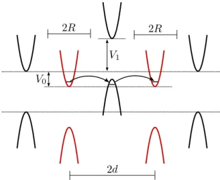
For the dot potentialV we use a barbell-like shape with circular disks, aligned along thex axis. The potential profile is defined by [r=(x,y)]
V(r)=V0ξdot(r)+V1max{|ξbar(r)| − |ξdot(r)|,0}, (2)
FIG. 1. (Color online) Illustration of the electrostatically defined graphene double dot. The top gates (colored/shaded regions) define the area of confinement, which can be adjusted for the circular dots via V0 (blue areas/circles) and the bridge between the dots viaV1
(red area/center) separately. In numerics, we terminate the grid at a distanceδbeyond the structure potential boundary, and we introduce a slightly increased mass at the edge of the grid (the outer black line).
with the left and right dot defined by
ξdot(r)=max{ξl(r),ξr(r)}, (3) where
ξl,r(r)= {1+exp[(rl,r−R)/β]}−1. (4) This represents two single dots with radius R, positioned at rl,r =r±(d,0), so that 2d is the interdot distance. The parameterβ is introduced to smoothen potential edges. The interdot barrier of widthwis described by
ξbar(r)= {1+exp[(−w/2−y)/β])}−1
× {1+exp[(y−w/2)/β]}−1
× {1+exp[(−d−x)/β]}−1
× {1+exp[(x−d)/β]}−1. (5) The geometry is shown in Fig. 1, and the potential V(r) [Eq. (2)] is sketched in Fig.2. The potentialV0represents the single dot confinement depth, whileV1sets the barrier height.
In experiments we envisage they are controllable individually by a corresponding local metallic gate, tuning them with respect to the global chemical potentialμ. For the following discussion we assume the graphene is undoped, so thatμis in the middle of the gap 2. We measure all energies from there (μ=0).
FIG. 2. (Color online) Illustrative plot of the potential landscape V(r) [Eq. (2)] for parametersV0= −V1andw=2R.
with typically 95 000 carbon atoms. The grid is extended by δ=25 nm around the potential barbell to ensure convergence.
The finite size of the grid in our numerical calculation leads to edge states at the boundary [21,28] that would not exist in an extended graphene sheet. To remove these artificial edge states from the calculated spectra, we introduce an additional mass term of 0.3 at the grid boundary (sketched by the black line in Fig.1). This trick improves the diagonalization times drastically, without any influence (as we checked) on the confined states we discuss here.
For the quantitative analysis we use the following material parameters. The hoppings aret =3090 meV, andt=0.05t.
The graphene lattice constant is 0.246 nm, and the mass is taken as=30 meV, according to Ref. [15]. Unless stated otherwise, we choose the structure parameters as follows:R = 25 nm,d =55 nm, andV0= −60 meV. The thickness of the barrier isw=2R, with a potential strengthV1to be specified.
ForV1=0 the barrier area potential is aligned with the bulk.
The smoothening parameter isβ=0.01R.
III. RESULTS: SINGLE DOT
First, we show how the confinement is created. We start with the example of a single dot that isd =0,V1=0 and consider only a variable depthV0. IfV0=0, the system is a sheet of graphene with a constant energy gap of 2=60 meV. States with energies|E|> are extended states of bulk graphene.
Consider nowV0is decreased. The conduction band is locally shifted towards lower energies, as shown in Fig.3, within the area set by the dot radiusR. Localized states with discrete energies inside the band gap appear [9]. This is analogous to ann-type dot in GaAs [33,36].
To describe the localized states spectrum, we define a set of characteristic energies, depicted in Fig.3. The ground-state energyε0is the energy difference betweenV0and the lowest localized state. The latter is separated from the first excited state by the excitation energyεex. The ionization energy, which we define as the minimal energy required for an excitation
FIG. 3. (Color online) Schematic energy diagram of a single dot.
Within the diameter of 2R, the energy bands are shifted by the confinement depthV0(this figure corresponds toV0<0). The ground state is offset from the band bottom by0(ground-state energy) from the nearest localized state byex (excitation energy) and from the nearest extended state byεion=min(ε,ε) (ionization energy).
-100 -80 -60 -40 -20 0 20 40 60 80 100 V0 [meV]
-30 -20 -10 0 10 20 30
energy [meV]
ε0 2Δ εex
ε"
ε’
FIG. 4. Calculated energy spectrum of a single dot as a function of the confinement depthV0. ForV0>0(V0<0), the holes (electrons) are localized in the dot. The gray regions represent extended states.
The characteristic energies are indicated.
from the localized ground state to an extended state, isεion= min(ε,ε), whereεandεare the energy differences between the localized ground state and the conduction and valence band edge, respectively.
Figure4shows the calculated energy spectrum of a single dot as a function of the confinement depthV0. The dot is ofn type forV0<0, andptype forV0>0, since the localized state is built from the lowest states of one (conduction) band, and the highest states of another (valence) band, respectively. Neglect- ing the small next-nearest neighbor hoppingt, the Hamilto- nian [Eq. (1)] has exact symmetryH(V ,B)→ −H(−V ,−B) upon replacement (ai,bi)→(bi,−ai). This translates into a one to one correspondence between low-energy holelike dot states at|V0|and electronlike states at−|V0|. From now on we therefore arbitrarily fixV0 negative. There is another, quasi-time-reversal, symmetry which connects states at theK valley with ones atKwith opposite total angular momentum Jz[37]. As a consequence, in zero magnetic field all states are twofold degenerate. In general, this degeneracy is a serious obstacle for quantum computation, as it impairs control over the exchange energy [36,38]. Fortunately, in graphene this degeneracy is split by a finite magnetic field (see below), which couples to the orbital momentumJz [13]. This is in contrast to the silicon-based dots, where such a direct control knob for the valley splitting does not exist.
Using the data from Fig. 4, we plot the characteristic energies in Fig. 5. We observe that the relative ground- state energy ε0 increases nonlinearly as the dot potential decreases, while the excitation energy εex, which is in our example only defined for V0−42.5 meV, is roughly con- stant. The ionization energyεionpeaks at aboutV0= −60 meV, where the ground state is exactly in the middle of the gap. Since we adopt a cylindrical potential shape in our model, the spectrum we obtain is rather different to the one usually met in semiconductor quantum dots with a harmonic confinement. There the energy levels are equidistant, and the ground-state energy is half of the excitation energy [39,40].
Also, here the lowest localized state hits the bulk band at about V0= −100 meV. The localized state then necessarily becomes occupied in undoped graphene and may easily hybridize with extended states. This is another difference to semiconductor
-100 -90 -80 -70 -60 -50 -40 -30 -20 -10 0 V0 [meV]
0 5 10 15 20 25 30 35 40
energy [meV]
ε0 εex εion
FIG. 5. Relative ground-state energyε0(dash-dot line), excitation energyεex(dashed line), and ionization energyεion(dotted line) as a function of the confinement depthV0.
quantum dots, where the equivalent energy scale is given by the band gap, which is of the order of a few eV [41].
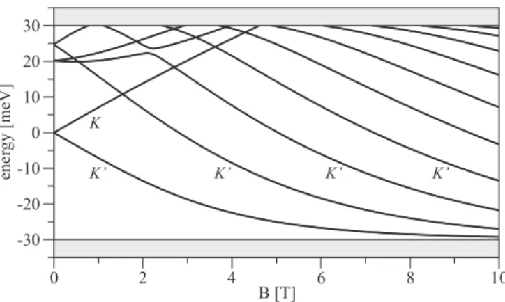
The energy spectrum as a function of a perpendicular mag- netic field is shown in Fig.6. The magnetic field lifts the valley degeneracy by breaking the time-reversal symmetry [13].
Landau levels tend to form [42]. For our dot parameters the magnetic lengthlB=√
/(eB) is of the order of the dot radius R for reasonable magnetic fields [26]. More precisely,lB is 81, 26, and 8 nm for a magnetic field of 0.1, 1, and 10 T, respectively, to be compared to a dot radius ofR=25 nm.
The “zero-mode” Landau level [13,43] forms at the valence band edge (−30 meV) fromKvalley states.
IV. RESULTS: DOUBLE DOT
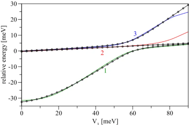
In this section we study the localized states in a double dot configuration [44–47]. The dot schematic energy diagram is shown in Fig.7. The corresponding spectrum, varying the barrier height while keeping the dots confinement depths fixed (V0= −60 meV), is in Fig. 8. Take first theV1=0 point.
Here the states in the left and right dots are well isolated by the barrier. The small remaining coupling splits the system eigenstates into symmetric and antisymmetric combinations of the single dot states. They are labeled as 2 and 3 in Fig.8,
0 2 4 6 8 10
B [T]
-30 -20 -10 0 10 20 30
energy [meV] K’
K
K’ K’ K’
FIG. 6. Calculated energy spectrum of a single dot (V0= −60 meV) as a function of a perpendicular magnetic field. The valley index of the lowest states is indicated byK/K.
FIG. 7. (Color online) Schematic energy diagram of a double dot.
The energy is shifted locally by V0 for the dots, and by V1 for the barrier (this figure corresponds toV0<0< V1). The interband tunneling from the left to the right dot via the barrier is indicated by black arrows.
and we define the tunneling energy as twice their energy difference [48]. The latter is one possible characterization of the interdot coupling [49] and in further we investigate the degree of control over it by electric and magnetic fields.
-100 -75 -50 -25 0 25 50 75 100 125
V1 [meV]
-30 -20 -10 0 10 20 30
energy [meV]
2T
3 2 1 (a)
-80 -60 -40 -20 0 20 40 60 80 100
V1 [meV]
0.1 1 10
T [meV]
(b)
FIG. 8. (Color online) (a) Calculated energy spectrum of a dou- ble dot (2d=110 nm,V0= −60 meV) as a function of the barrier potentialV1. The red (2) and blue (3) lines denote the dot ground state and the first excited state, respectively. Half of their energy difference is the tunneling energy T. The shaded region between those two states and the vertical line at V1=0 are a guide for the eye. The green curve (1) denotes the highest localized state of the barrier. The dashed line is the top line forV0>0 from Fig.4. (b) The tunneling energy replotted from the data in (a). Line with symbols is a fit from the model described below Eq. (6).
Consider first lowering the barrier between the dots by making V1 negative. The tunneling energy increases due to increasing quantum mechanical overlap of isolated dot eigenstates. In the same time, the energy distance to the next orbital level decreases. This is expected, as at V1∼V0 =
−60 meV the system resembles more a prolongated single dot, rather than a tunnel coupled double dot. For even larger negativeV1 the lowest states are more and more localized in the barrier itself and the system qualitatively changes back to a single dot—the tunneling energy saturates and energy distance to the next level increases. This behavior, referred to as thennncoupling [50], is analogous to a GaAs dot.
B. Coupling minimum
Consider now that, starting again from zero,V1is increased.
In GaAs, such an increase of the barrier between the two dots makes the tunneling smaller (exponentially). Such high sensi- tivity of the interdot coupling to electrostatic potential [51,52]
is at the heart of the versatile control of spin qubits in GaAs dots. Looking at Fig.8(b), however, a decrease in tunneling withV1 is very modest and soon changes into an increase (the tunneling reaches minimum at V1=6 meV, which is 3μeV below its value of 110μeV atV1=0). This turn in trend is caused by the presence of thep-like (valence) states localized inside the barrier [9], through which then-like dot states are coupled effectively. This is referred to as thenpn coupling [23,50]. The arising limit-from-below on the interdot coupling, which can be considered as the manifestation of the Klein paradox [12], then possibly imposes a serious limitation on the extent of control over the double dot states. It is important to understand what parameters set the achievable coupling minimum.
We expect the minimum to occur, very roughly, when the dot confined state is energetically halfway between the barrier conduction and valence bands. For our parameter V0= −60 meV, resulting in0=30 meV, this estimate gives the minimum atV1=0, which is close to the value observed in numerics. The value of the minimal tunneling will decrease with the barrier height and length. The former is proportional to the induced mass , while the latter is given by the interdot distance. This is confirmed in Fig.9, where a drop of tunneling with the interdot distance is demonstrated. Al- ternatively to changing the electrostatic barrier, the tunneling can be suppressed by a perpendicular magnetic field [53].
Localization of electrons by its orbital effects, demonstrated by the tunneling suppression, was studied in detail in GaAs [52]
and silicon [54] quantum dots. Our expectation of an analogous behavior in graphene is confirmed by numerical results, shown in Fig.10. There it is shown that the perpendicular field of few Tesla suppresses the tunneling by 1–2 orders of magnitude, depending on the barrier potential.
C. npncoupling
Let us finish the analysis of the effects of the barrier potential V1, now considering the npn coupling regime. It is signaled by a change in the trend of the interdot coupling, which starts to increase upon increasing the barrier height. In
50 60 70 80 90 100 110 120 interdot distance 2d [nm]
-10 0 10 20 30
energy [meV] 2T
FIG. 9. (Color online) Calculated energy spectrum of a double dot (V0= −60 meV,V1=0) as a function of the interdot distance 2d. The red and blue curves give the localized ground and first excited state, respectively. The tunneling energyT is indicated.
Fig.8this happens atV1 ≈6 meV. Beyond this point, the left and right single dots are coupled most effectively through the p-like localized state formed in the barrier, tagged as line 1 in Fig.8(a). In this regime the double dot low-energy spectrum is well characterized considering three states (the left dot, the right dot, and the barrier), with the neighboring pairs coupled by a tunneling matrix elementτ. To demonstrate this, we replot the three energies from Fig.8 into Fig.11and fit them with the spectrum of the following Hamiltonian:
H =
⎛
⎜⎝
0 τ 0
τ ε τ
0 τ 0
⎞
⎟⎠. (6)
First, the energy offset of the p state is well approximated by the single dot ground-state energy (V1)≈ −+V1− 0(V1). This is shown by plotting the approximation (that is, the top line for V0>0 from Fig.4) as a dashed line in Fig. 8(a). We note that this is rather a coincidence, as the effective dot shape of thepregion is different from the single dot considered before (though both of these energies should indeed scale similarly, as the areas of the dot and the barrier are comparable in our model). However, for our purpose of extracting the tunneling matrix elementτ we can still make
0 0.5 1 1.5 2 2.5 3 3.5
B [T]
0.01 0.1 1
tunneling energy T [meV] V1 = -50 meV
V1 = 0 meV
FIG. 10. Calculated tunneling energyT for a graphene double dot (2d=110 nm,V0= −60 meV) as a function of perpendicular magnetic field for two values of the barrier potential.
0 20 40 60 80
V1 [meV]
-30 -20 -10 0 10 20 30
relative energy [meV]
1 2
3
FIG. 11. (Color online) Eigenenergies of the states 1, 2, and 3, taken from Fig. 8 (solid lines) and from the analytical model, described below Eq. (6) (lines with circles). A linear trend δ= 0.0593V1, fitted from the exact values of the level 2 energy, was added to all fitted values.
use of this fact and need not fit the energy offset of the p state separately. Second, the tunneling matrix element τ is obtained from the width of the anticrossing of lines 1 and 3 [at V1≈60 meV in Fig.8(a)], from where we getτ ≈2.5 meV.
With this, basically a single parameter fit, we obtain a very good agreement with the exact numerics, as seen in Fig.11, not only close to the anticrossing, but through out the whole npn regime. The model starts to deviate only once higher excitedp states in the barrier anticross with the n-like dot states (beyondV170 meV). The correspondence for lower V1is demonstrated by comparing the exact tunneling energy with the one obtained from our model [Eq. (6)], which we do in Fig.8(b). Since at its minimum the tunneling energy does not differ from the model by more than a factor of two, we estimate that throughout thenpn regionτ does not vary more than by a factor of 1/√
2. This stability of the tunneling matrix element over a very large range of gate voltages is perhaps surprising, but welcomed as it justifies the analysis of the double dot structure in terms of isolated eigenstates of the dots and the barrier.
We finish with a note that the system in thenpnregime seems well suited for adiabatic passage protocols [55–57].
Namely, these are based on a Hamiltonian such as Eq. (6) if one can control the two matrix elements independently. Such a control might be possible using an electric fieldEapplied along the dot axis, which changes the Hamiltonian from Eq. (6) into
H =
⎛
⎜⎝
−eEd τ 0
τ ε τ
0 τ eEd
⎞
⎟⎠. (7)
The important feature is that the electric field shifts the dot and barrier states in opposite directions, as they aren- andp-like, respectively. This will change the tunneling matrix elements in an asymmetric way, e.g.,τ> τ > τ. Based on numerical results (not shown) we find that, unfortunately, in our model the single dot confinement edges are so steep that the electric field induced asymmetry inτ is too small compared to the
±
passage protocols. Namely, the latter require an efficient way to independently tuneτandτ, well into the limitsτ τ andττ, and without simultaneously inducing substantial energy offsets between the states. Other potential profiles might be better suited for this task.
V. CONCLUSIONS
We investigated the energy spectrum of gated single and laterally coupled double quantum dots in gapped graphene. For the single dot, we presented the characteristic energies of the localized states: the ground-state energy, the excitation energy, and the ionization energy. We also showed the influence of a perpendicular magnetic field, including the lifting of the valley degeneracy.
We primarily focused on the interdot coupling in a double dot configuration, the control over which is crucial for few electron quantum dot states manipulations. The extent of the electrical control over the electron tunneling in graphene isa priori not clear, because of the Klein tunneling effect. Our
overcome in gapped graphene and the interdot tunneling can be varied, for reasonable parameters, by orders of magnitude. The most important difference to a GaAs dot is that in a graphene dot there is a minimum below which the tunneling cannot be reduced. This is due to the presence of states localized in the barrier, what can be seen as an artifact of the Klein tunneling. The achievable coupling minimum is set by the dot geometry and the substrate-induced gap. For these parameters fixed, the tunneling can be further reduced by a perpendicular magnetic field. The presence of the states in the barrier, on the other hand, offers new regimes of operation, unaccessible to GaAs material, such as thenpndouble dot.
ACKNOWLEDGMENTS
We would like to thank Jan Bundesmann and Sebas- tian Lautenschlager for useful discussions. This work was supported by DFG under Grants No. SPP 1285 and No.
SFB 689. P.S. acknowledges support from QUTE and COQI APVV-0646-10.
[1] A. K. Geim and K. S. Novoselov,Nat. Mater.6,183(2007).
[2] P. Avouris, Z. Chen, and V. Perebeinos,Nat. Nano.2,605(2007).
[3] A. H. Castro Neto, F. Guinea, N. M. R. Peres, K. S. Novoselov, and A. K. Geim,Rev. Mod. Phys.81,109(2009).
[4] D. Abergel, V. Apalkov, J. Berashevich, K. Ziegler, and T. Chakraborty,Adv. Phys.59,261(2010).
[5] Y.-M. Lin, C. Dimitrakopoulos, K. A. Jenkins, D. B. Farmer, H.-Y. Chiu, A. Grill, and P. Avouris,Science327,662(2010).
[6] Y. Wu, Y. ming Lin, A. A. Bol, K. A. Jenkins, F. Xia, D. B.
Farmer, Y. Zhu, and P. Avouris,Nature (London)472,74(2011).
[7] K. S. Novoselov, A. K. Geim, S. V. Morozov, D. Jiang, Y. Zhang, S. V. Dubonos, I. V. Grigorieva, and A. A. Firsov,Science306, 666(2004).
[8] K. S. Novoselov, D. Jiang, F. Schedin, T. J. Booth, V. V.
Khotkevich, S. V. Morozov, and A. K. Geim,Proc. Natl. Acad.
Sci. USA102,10451(2005).
[9] B. Trauzettel, D. V. Bulaev, D. Loss, and G. Burkard,Nat. Phys.
3,192(2007).
[10] G.-P. Guo, Z.-R. Lin, T. Tu, G. Cao, X.-P. Li, and G.-C. Guo, New J. Phys.11,123005(2009).
[11] P. Recher and B. Trauzettel,Nanotechnology21,302001(2010).
[12] A. Calogeracos and N. Dombey,Contemp. Phys.40,313(1999).
[13] P. Recher, J. Nilsson, G. Burkard, and B. Trauzettel,Phys. Rev.
B79,085407(2009).
[14] P. G. Silvestrov and K. B. Efetov,Phys. Rev. Lett.98,016802 (2007).
[15] G. Giovannetti, P. A. Khomyakov, G. Brocks, P. J. Kelly, and J. van den Brink,Phys. Rev. B76,073103(2007).
[16] S. Y. Zhou, G.-H. Gweon, A. V. Fedorov, P. N. First, W. A. de Heer, D.-H. Lee, F. Guinea, A. H. Castro Neto, and A. Lanzara, Nat. Mater.6,770(2007).
[17] C. Stampfer, J. Guttinger, F. Molitor, D. Graf, T. Ihn, and K. Ensslin,Appl. Phys. Lett.92,012102(2008).
[18] L. A. Ponomarenko, F. Schedin, M. I. Katsnelson, R. Yang, E. W. Hill, K. S. Novoselov, and A. K. Geim,Science320,356 (2008).
[19] D. K¨olbl and D. M. Zumb¨uhl,arXiv:1307.8163.
[20] E. McCann and V. I. Falko,J. Phys.: Condens. Matter16,2371 (2004).
[21] A. R. Akhmerov and C. W. J. Beenakker,Phys. Rev. B77, 085423(2008).
[22] M. Vanevi´c, V. M. Stojanovi´c, and M. Kindermann,Phys. Rev.
B80,045410(2009).
[23] A. Rozhkov, G. Giavaras, Y. P. Bliokh, V. Freilikher, and F. Nori, Phys. Rep.503,77(2011).
[24] J. Guttinger, F. Molitor, C. Stampfer, S. Schnez, A. Jacobsen, S. Droescher, T. Ihn, and K. Ensslin,Rep. Prog. Phys.75,126502 (2012).
[25] M. Gruji´c, M. Zarenia, A. Chaves, M. Tadi´c, G. A. Farias, and F. M. Peeters,Phys. Rev. B84,205441(2011).
[26] S. Schnez, K. Ensslin, M. Sigrist, and T. Ihn,Phys. Rev. B78, 195427(2008).
[27] J. G¨uttinger, T. Frey, C. Stampfer, T. Ihn, and K. Ensslin, Phys. Rev. Lett.105,116801(2010).
[28] M. Wimmer, A. R. Akhmerov, and F. Guinea,Phys. Rev. B82, 045409(2010).
[29] M. Zarenia, A. Chaves, G. A. Farias, and F. M. Peeters, Phys. Rev. B84,245403(2011).
[30] C. H. Bennett and D. P. DiVincenzo,Nature (London)404,247 (2000).
[31] D. Loss and D. P. DiVincenzo,Phys. Rev. A57,120(1998).
[32] D. Wei, H.-O. Li, G. Cao, G. Luo, Z.-X. Zheng, T. Tu, M. Xiao, G.-C. Guo, H.-W. Jiang, and G.-P. Guo,Sci. Rep.3,3175(2013).
[33] R. Hanson, L. P. Kouwenhoven, J. R. Petta, S. Tarucha, and L. M. K. Vandersypen,Rev. Mod. Phys.79,1217(2007).
[34] C. Kloeffel and D. Loss,Annu. Rev. Condens. Matter Phys.4, 51(2013).
[35] R. Peierls,Z. Phys.80,763(1933).
[36] F. A. Zwanenburg, A. S. Dzurak, A. Morello, M. Y. Simmons, L. C. L. Hollenberg, G. Klimeck, S. Rogge, S. N. Coppersmith, and M. A. Eriksson,Rev. Mod. Phys.85,961(2013).
[37] C. W. J. Beenakker,Rev. Mod. Phys.80,1337(2008).
[38] D. Culcer, Ł. Cywinski, Q. Li, X. Hu, and S. Das Sarma, Phys. Rev. B80,205302(2009).
[39] T. Chakraborty,Quantum Dots, 1st ed. (Elsevier, New York, 1999).
[40] Q. Li, Ł. Cywinski, D. Culcer, X. Hu, and S. Das Sarma, Phys. Rev. B81,085313(2010).
[41] P. Y. Yu and M. Cardona,Fundamentals of Semiconductors:
Physics and Materials Properties, 3rd ed. (Springer, Berlin, 2005).
[42] H.-Y. Chen, V. Apalkov, and T. Chakraborty,Phys. Rev. Lett.
98,186803(2007).
[43] F. D. M. Haldane,Phys. Rev. Lett.61,2015(1988).
[44] S. Moriyama, D. Tsuya, E. Watanabe, S. Uji, M. Shimizu, T.
Mori, T. Yamaguchi, and K. Ishibashi,Nano Lett.9,2891(2009).
[45] X. L. Liu, D. Hug, and L. M. K. Vandersypen,Nano Lett.10, 1623(2010).
[46] F. Molitor, H. Knowles, S. Droescher, U. Gasser, T. Choi, P. Roulleau, J. Guttinger, A. Jacobsen, C. Stampfer, K. Ensslin, and T. Ihn,Europhys. Lett.89,67005(2010).
[47] L.-J. Wang, H.-O. Li, T. Tu, G. Cao, C. Zhou, X.-J. Hao, Z. Su, M. Xiao, G.-C. Guo, A. M. Chang, and G.-P. Guo,Appl. Phys.
Lett.100,022106(2012).
[48] We note that for configurations whereV1< V0there is no barrier in the middle of the dot, and thus the transport of an electron between the single dots happens ballistically, rather than by tunneling. However, as there is no ambiguity in this energy definition, we stick to the name.
[49] F. Baruffa, P. Stano, and J. Fabian,Phys. Rev. Lett.104,126401 (2010).
[50] X. Liu, J. B. Oostinga, A. F. Morpurgo, and L. M. K.
Vandersypen,Phys. Rev. B80,121407(2009).
[51] L. P. Gorkov and P. L. Krotkov,Phys. Rev. B68,155206(2003).
[52] P. Stano and J. Fabian,Phys. Rev. B72,155410(2005).
[53] An inhomogeneous magnetic field can even provide for a complete confinement, see Ref. [58].
[54] M. Raith, P. Stano, and J. Fabian,Phys. Rev. B 83, 195318 (2011).
[55] A. D. Greentree, J. H. Cole, A. R. Hamilton, and L. C. L.
Hollenberg,Phys. Rev. B70,235317(2004).
[56] J. Fabian and U. Hohenester,Phys. Rev. B72,201304(R)(2005).
[57] J. H. Cole, A. D. Greentree, L. C. L. Hollenberg, and S. Das Sarma,Phys. Rev. B77,235418(2008).
[58] A. De Martino, L. Dell’Anna, and R. Egger,Phys. Rev. Lett.98, 066802(2007).
![FIG. 2. (Color online) Illustrative plot of the potential landscape V (r) [Eq. (2)] for parameters V 0 = −V 1 and w = 2R.](https://thumb-eu.123doks.com/thumbv2/1library_info/5619905.1692081/2.911.493.819.804.1019/fig-color-online-illustrative-plot-potential-landscape-parameters.webp)