Electric Field Control of Spin Lifetimes in Nb - SrTiO
3by Spin-Orbit Fields
A. M. Kamerbeek,1,*P. Högl,2 J. Fabian,2and T. Banerjee1
1Physics of Nanodevices, Zernike Institute for Advanced Materials, University of Groningen, Nijenborgh 4, 9747 AG Groningen, Netherlands
2Institute for Theoretical Physics, University of Regensburg, 93040 Regensburg, Germany
(Received 21 May 2015; revised manuscript received 14 July 2015; published 24 September 2015) We show electric field control of the spin accumulation at the interface of the oxide semiconductor Nb-SrTiO3with Co=AlOxspin injection contacts at room temperature. The in-plane spin lifetimeτ∥, as well as the ratio of the out-of-plane to in-plane spin lifetimeτ⊥=τ∥, is manipulated by the built-in electric field at the semiconductor surface, without any additional gate contact. The origin of this manipulation is attributed to Rashba spin orbit fields (SOFs) at the Nb-SrTiO3surface and shown to be consistent with theoretical model calculations based on SOF spin flip scattering. Additionally, the junction can be set in a high or low resistance state, leading to a nonvolatile control ofτ⊥=τ∥, consistent with the manipulation of the Rashba SOF strength.
Such room temperature electric field control over the spin state is essential for developing energy-efficient spintronic devices and shows promise for complex oxide based (spin) electronics.
DOI:10.1103/PhysRevLett.115.136601 PACS numbers: 72.25.-b, 73.40.-c, 85.75.Hh
Recent demonstrations of electrical injection and detec- tion of spin accumulation in conventional semiconductors enhances the prospects for realizing a spin-based field- effect transistor (SFET) [1–5]. A key requirement for SFETs is the possibility to manipulate spin transport in the semiconducting channel by an electric field, at room temperature, which to date remains elusive. An attractive way to realize this is the integration of a gate electrode which tunes the spin-orbit coupling in the semiconducting channel via an electric field perpendicular to it[6,7]. In this context, the emerging class of oxide materials and their heterostructures provide an attractive platform for design- ing electronic interfaces [8–11]. Exploiting their intrinsic correlation effects allows tuning of key transport properties such as charge density, mobility, permittivity, and ferro- magnetism, essential for the electric field tuning of (spin) electronic transport. Although electric control of magnet- ism in engineered interfaces of oxide materials has been predicted and demonstrated[12,13], electric field control of spin transport in oxide semiconductors is largely unex- plored, in spite of theoretical predictions of long spin lifetimes inn-doped SrTiO3 [14].
In this work, we demonstrate a strong influence of the built-in electric field, close to the interface, on the spin lifetimes in an oxide semiconductor—Nb-doped SrTiO3. Semiconducting SrTiO3 is a commonly used substrate in oxide electronics and exhibits much richer electronic states, as compared to conventionalp-band semiconductors, due to the narrow bandwidth of the d-orbital derived conduction bands. We observe a strong dependence of the Hanle line shape on the applied bias, unlike in other electrical injection and detection experiments with conventional semiconduc- tors such as Si, Ge, or GaAs, using a three-terminal geometry [3,4,15]. We find that the extracted in-plane spin lifetime
changes by an order of magnitude from 3 to 15 ps, with decreasing electric field strength at the spin injection inter- face. Similarly, the spin voltage anisotropy V⊥=V∥ (the voltage generated by out-of-plane V⊥ over in-plane spins V∥) exhibits a systematically increasing trend (from 0.5 to 0.75) when decreasing the interface electric field. These observations are shown to be consistent with a theoretical model, where the spin lifetime is determined by spin flip events due to a Rashba spin orbit field (SOF). We further demonstrate, the possibility to modestly modulate the SOF strength, by using the electroresistance effect prevalent at metal=Nb−SrTiO3 interfaces. These results are a first demonstration of realizing control (via an electric field tuned SOF) over the spin accumulation in a semiconductor at room temperature, a vital ingredient for spin logic.
For this work, 0.1 wt% Nb-doped SrTiO3 (Nb-SrTiO3) single crystal substrates from Crystec GmbH are used.
SrTiO3 has a perovskite crystal structure which becomes n-type conducting by doping Nb5þ at the Ti4þ site. The crystal has a very large permittivity ϵr of ∼300 at room temperature and is a nonlinear dielectric[16]. Typical room temperature mobilities are10cm2=V s which results in a charge diffusion constantDcof around0.2cm2=s using the Einstein relation σ¼nqμ¼q2νDc with n the charge carrier density, μ the mobility, and νðEÞ the density of state¼0.615states=Ry · cel (obtained from Ref. [17]).
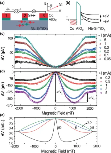
The measurement schematic of the three-terminal geom- etry is shown in Fig.1(a). Prior to deposition of the spin injection contacts of Co=AlOx in ane-beam evaporator an in situO2plasma is used to clean the Nb-SrTiO3surface.
The spin injection contacts are formed by∼10Å Al, which isin situplasma oxidized followed by subsequent growth of 20 nm of Co. The contact sizes range from50×200up to200×200μm2and are separated by at least100μm. A
sketch of the energy landscape at the interface is given in Fig. 1(b). The charge transport across the junction is dominated by field emission through the tunnel barrier and Schottky barrier [18].
Room temperature Hanle measurements are performed by sourcing a constant bias current between contact 1 and 2 and measuring the change in voltage between contacts 2 and 3 while applying a perpendicular to plane magnetic field. At zero field the injected spins point in-plane due to the in-plane magnetization of Co. The results are shown in Fig. 1(c) for negative current bias (spin injection) and Fig.1(d) for positive current bias (spin extraction).
As shown in Fig.1(d), with increasing positive bias the line shape shows a systematic trend of narrowing. In this regime an upturn of the spin voltage starts to appear at higher fields, (as marked byV⊥), while this is not observed at low positive bias or negative bias. The applied field rotates the
magnetization of Cobalt out of plane (completed around 1800 mT) which coincides with saturation of the line shape.
When spin drift is neglected, the change of the spin voltage in a three-terminal Hanle measurement can be described as follows:
ΔV¼V⊥cos2ðθÞ þV∥sin2ðθÞ ffiffiffi2 p
ffiffiffiffiffiffiffiffiffiffiffiffiffiffiffiffiffiffiffiffiffiffiffiffiffiffiffiffiffiffiffiffiffiffiffi 1þ ffiffiffiffiffiffiffiffiffiffiffiffiffiffiffiffiffiffiffiffiffiffiffi 1þ ðωLτ∥Þ2 q
1þ ðωLτ∥Þ2 vu
ut
; ð1Þ
with ωL¼ ðegB=2mÞ, the Larmor precession term (g¼2; m¼me),θ¼θðBÞthe angle between the surface normal and the magnetization vector of cobalt which is a function of the applied magnetic field [see Fig.1(a), right top], τ∥ the in-plane spin lifetime, V⊥ and V∥ the spin voltage developed by the out- and in-plane spin accumu- lation, respectively. The out(in)-plane spin voltage is given byV⊥;∥¼P2Rsλ⊥;∥sf =2Wwith the out(in)-plane spin relax- ation lengthλ⊥;∥sf ¼ ffiffiffiffiffiffiffiffiffiffiffiffiffi
Dsτ⊥;∥
p andW the contact width. If the polarization of the electronP and the sheet resistance RS do not strongly depend on magnetic field the relation between spin voltage and spin lifetime anisotropy becomes V⊥=V∥¼ ffiffiffiffiffiffiffiffiffiffiffiffi
τ⊥=τ∥
p . The solid lines in Fig.1are fits using Eq.(1) which show good agreement with the data.
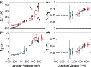
The fit values forτ∥, V∥, V⊥and their ratio are plotted as a function of the junction voltage as shown in Fig.2. We plot the extracted parameters against junction voltage instead of bias current as the junction voltage relates to the electric field at the interface. Both the in- and out-of- plane spin voltage show a superlinear trend for increasing positive voltage while a saturating (smaller) spin voltage is observed at negative voltage [Fig.2(a)]. This is consistent with the observed change ofτ∥as shown in Fig. 2(b). To obtain an order of magnitude estimate ofλ∥we can assume Ds¼Dc and find it is around 10 nm. The spin voltage anisotropy, defined as V⊥=V∥, at positive bias shows an increasing trend with positive junction voltage and saturates aroundþ500mV [Fig.2(c)]. As the fit to the Hanle line shape is quite insensitive to a large change in the anisotropy ratio both at low positive and negative bias there is no clear restriction on the fit ratio of V⊥=V∥ (hence the increased error at low positive bias). Given the trend in Fig.2(c)we have set V⊥ ¼0.5V∥ at negative bias which can be considered as the upper limit of the ratio (see Supplemental Material [19]for details).
Note that Eq. (1) implies that for low spin lifetimes (τ∥≪ωLjB¼MS) the cobalt magnetization is rotated from in to out of plane by the magnetic field while the spins are hardly dephased. Therefore the voltage purely reflects the difference in spin voltage generated by in- versus out-of- plane spins. To illustrate this, we have simulated the change of the line shape using Eq.(1)in Fig.1(e). We vary the in- plane spin lifetime from 50, 5, 2.5 to 0.5 ps, set V⊥ ¼ 0.5V∥ and the saturation magnetization MS of the cobalt electrode at 1800 mT. The overall shape corresponds very well to the observed behavior in Figs.1(c) and1(d).
FIG. 1 (color online). (a) Three-terminal device schematic, right top defines the angleθ as in Eq.(1). (b) Potential energy diagram at the spin injection interface. (c) Three-terminal Hanle measurements at negative bias and (d) at positive bias. Narrowing of the linewidth and the appearance of an upturn inΔVat higher magnetic fields is observed with increasing positive bias. Around 1800 mTΔV saturates asMhas rotated out of plane. (e) Sim- ulation of Hanle measurement using Eq.(1)shows good agree- ment with the observed trend in panels (c) and (d) when assuming a changing spin lifetime. The numbers are the spin lifetime in ps used to simulate the line shapes.
The observed response as shown in Fig. 2 is different from the findings in Si, Ge, or GaAs [3,4,15] and even those based on oxides such as the LaAlO3=SrTiO32 DEG or highly n-doped SrTiO3 [21–23]. From the Hanle measurements, we observe a linewidth which is an order of magnitude broader and interestingly, exhibits a system- atic evolution over the measured bias range. This system- atic change of the in-plane spin lifetime and spin voltage anisotropy with junction voltage was not reported in earlier studies. Recently, it has also been shown that a Lorentzian magnetoresistance effect can occur when charge transport occurs via defect states inside the tunnel barrier in the presence of random local magnetic fields[24]. We employ similar Co=AlOx contacts but observe much broader line- widths and systematic line shape changes with bias.
Therefore, we attribute the observed response to spin accumulation in the semiconductor (see Supplemental Material [19]for an extended discussion).
We believe that in our devices, the observed response deviates from the reported works due to the difference of the potential landscape at the spin injection interface. We have tailored the interface such that an appreciable built-in electric field exists at the semiconductor surface due to the thin Schottky barrier. This field can be increased or decreased by applying a negative or positive bias to the junction [see Fig. 1(b)]. Increase of the spin lifetime due to spin drift effects are ruled out as the lifetime should increase with reverse bias, opposite to what we observe [25–28].
The observed increase ofτ∥andτ⊥=τ∥with bias occurs when decreasing the electric field strength at the interface.
The most likely mechanism driving such changes is SOFs.
Large (electric field tunable) Rashba effects have been observed for 2DEGs at the LaAlO3=SrTiO3 interface or
SrTiO3surface[29–31]. Because of breaking of the crystal inversion symmetry, it is expected that a Rashba-like SOF is also present at such spin injection interfaces. To ascertain the influence of Rashba SOFs at the interface, we consider a model with ferromagnet (z <0Þand normal metal (z >0) semi-infinite regions separated by a flat interface atz¼0, with potential barrier and spin-orbit coupling (SOC) scattering [19]. From the model we extract spin-flip probabilities for electrons tunneling through the interface.
These results are indicative of the experimentally observed spin dephasing of steady state spin accumulation induced by Rashba SOFs and allow a qualitative comparison of the main trends of characteristic quantities. The model Hamiltonian readsH¼H0þHB with
H0¼−ℏ2 2 ∇
1
mðzÞ
∇−μðzÞ−Δxc
2 Θð−zÞm·σˆ; ð2Þ where H0 contains the kinetic energy and the Zeeman splitting in the ferromagnet. The unit magnetization vector is m¼ ½sinΘcosΦ;sinΘsinΦ;cosΘ, σˆ are the Pauli matrices, Δxc is the exchange spin splitting in the ferro- magnet (Stoner model),mðzÞis the effective mass, andμðzÞ the chemical potential. The interfacial scattering is modeled asHB¼ ðV0dþw·σÞδðˆ zÞ, whereV0anddare the barrier height and width [32], while w¼αðky;−kx;0Þ is the Rashba SOC field [33,34]. For simplicity, we consider equal Fermi wave vectorkFand massmin all regions[19].
The normalized spin-flip probability current along the interface is[19]
Jsf ¼P jtr−σ jtrσ þjtr−σ
σ¼↑þ ð1−PÞ jtr−σ jtrσ þjtr−σ
σ¼↓ ð3Þ with the spin polarization P¼ ðΔxc=2Þ=μF with μF the chemical potential in the ferromagnet and the transmitted probability currentjtrσ, whereσ¼↑ð↓Þcorresponds to spin parallel (anti-parallel) tomˆ. The strength of the potential barrier is denoted byZ¼V0dm=ðℏ2kFÞand the strength of Rashba SOC byλα¼2αm=ℏ2.
The calculated spin-flip currents are shown in Fig. 3.
With increasing SOC the spin-flip current first slowly increases, shows a rapid upturn, and finally saturates.
The transitions at certain λα between these three trends depend on the potential barrierZ. In our experiments, the tunnel barrier employed corresponds toZ≈10[35]. Using the proportionality of spin-flip current and spin-flip rate, Jsf∼1=τ, we compare the calculated trend to the experi- ment (inset Fig.3). An increase of 1=τ is observed when going from positive to negative junction voltage, corre- sponding to an increase of the interface electric field. The similar trend of the model calculations and the experimen- tal1=τplot strongly indicates the presence of Rashba SOFs which are amplified by the applied voltage. In the model we tune the SOC strength by the phenomenological parameter λα [19].
(a)
(b)
(c)
(d)
FIG. 2 (color online). Spin voltages and lifetime obtained from fits to Hanle data from several devices as a function of junction voltage. (a) In-plane (V∥) and out-of-plane (V⊥) spin voltage.
(b) In-plane spin lifetimeτ∥. (c) The ratio of the out/in-plane spin voltage. (d) The spin lifetime anisotropy. It increases systemati- cally with junction voltage. Different symbols represents data from different devices in panels (b), (c), and (d).
This hypothesis is further strengthened by the anisotropy of the spin lifetimeτ⊥=τ∥. In absence of a Rashba SOF a ratio τ⊥=τ∥¼1 is expected while the theoretical minimum, at strong Rashba SOFs, is τ⊥=τ∥¼0.5. As shown in Fig.2(d)τ⊥=τ∥indeed exhibits an increase from∼0.25to 0.55 consistent with a decreasing SOF strength. The ratio, however, is largely below the theoretical limit of 0.5, indicating other anisotropic spin dephasing mechanisms to be present. A possible candidate is an intrinsic in-plane magnetic field component at the Nb-SrTiO3surface. There is considerable evidence for such room temperature inter- face magnetism in related systems[10,36–38]. We want to point out that using the standard Lorentzian form of the spin dephasing expression in Eq.(1), commonly used for three- terminal geometries[3], does not affect the trend of the spin lifetime anisotropy but shifts the ratio down over the whole range by∼0.125. The presence of a superimposed tunneling anisotropic magnetoresistance could also shift the ratio.
Such a pronounced effect of a Rashba-like SOF on the spin accumulation could originate from a large Rashba coefficient α. However, due to the electron correlation effects in SrTiO3 other factors might also play a role and lead to an enhanced sensitivity on a SOF. For instance, we believe most charge diffusion to occur in thex-yplane even though the electrons are not confined in thezdirection due to the band dispersion close to the Fermi level. The conduction bands of n-doped SrTiO3 consist of the t2g state derived from the dxy;yz;xz orbitals of the Ti. In bulk these orbitals are degenerate but at an interface this degeneracy can be lifted. [10,39,40]. The dxy band is shown to move down in energy while the dyz;xz orbitals move up. Thedxyderived band has light effective mass in thex-yplane and heavy effective mass along thezdirection [39,41]. Because of the very short spin relaxation length most of the spin voltage is generated in this near interface region and the strong anisotropy of the effective masses causes predominant diffusion of the spins in thex-yplane.
Finally, we demonstrate the ability to manipulate the spin accumulation using the electroresistance effect present in the junction. Such electroresistance effects, where the junction resistance can be switched from high to low, are well known to occur in metal=Nb-SrTiO3 junctions [42]. In the pristine state the device is in the high resistance state (HRS). It can be switched back and forth between a low resistance state (LRS) and HRS by applying a large positive or negative bias, respectively. Hanle measurements at the same current bias (þ7.5mA) in the LRS and HRS are shown in Fig.4(a). A clear modulation of the Hanle line shape is observed. Fits to the Hanle data using Eq.(1)show a systematic increase of the spin lifetime anisotropy as shown in Fig. 4(b). The increased voltage in the HRS decreases the electric field at the interface as it effectively acts as an added positive bias. The increase of the ratio is in line with a decreased SOF strength and indicates a nonvolatile way of controlling the Rashba SOFs. In Fig. 4(c) the ratios of the values in Fig. 4(b) are shown (i.e., the ratio of τ⊥=τ∥ for the HRS over LRS). The effectiveness of electroresistive control reduces at higher bias consistent with Figs.2(b)and2(c). (see Supplemental Material[19] for details).
We demonstrate a wide tunability of the spin accumu- lation, achieved by the built-in electric field in an oxide semiconductor, Nb-SrTiO3, at room temperature, without any additional design complexity of a gate contact. We show that the manipulation of the built-in electric field leads to a large change in the spin lifetime and its anisotropy which we explain with the field tuning of the Rashba SOF strength. The general trends are confirmed by FIG. 3 (color online). Calculated normalized spin-flip current
Jsf as a function of Rashba spin-orbit coupling λα. In-plane (dashed lines) and out-of-plane (solid lines) magnetization with spin polarization P¼0.4 and bias voltage eV=μF¼0.05 for different barrier potentialZ. Inset: Experimental in-plane spin- flip rate 1=τ∥. Reducing the junction voltage from positive to negative increases the internal electric field.
FIG. 4 (color online). (a) Three terminal Hanle measurements in the low (squares) and high (circles) resistance state atþ7.5mA. A clear modification of the Hanle line shape is observed. (b) Ratio of the out-of-plane/in-plane spin lifetimes as a function of bias current. A clear systematic increase of the ratio is observed when the junction is set to the high resistance state. (c) The ratio of HRS over LRSτ⊥=τ∥as in (b). At larger bias currents the electroresistive control over the spin lifetime reduces consistent with Figs.1(b) and1(d)(dotted line is a guide to the eye).
a theoretical spin-flip model based on interfacial spin-orbit fields. The strong SOF effects on the electron spins in SrTiO3show promise for electric field control over the spin state, a prerequisite for developing a SFET.
A. M. K. and T. B. acknowledge financial support from the Netherlands Organization for Scientific Research NWO- VIDI program and the Rosalind Franklin Fellowship.
*a.m.kamerbeek@rug.nl
[1] X. Lou, C. Adelmann, S. A. Crooker, E. S. Garlid, J. Zhang, K. S. M. Reddy, S. D. Flexner, C. J. Palmstrøm, and P. A.
Crowell,Nat. Phys.3, 197 (2007).
[2] I. Appelbaum, B. Huang, and D. J. Monsma, Nature (London)447, 295 (2007).
[3] S. P. Dash, S. Sharma, R. S. Patel, M. P. de Jong, and R.
Jansen,Nature (London)462, 491 (2009).
[4] L.-T. Chang, W. Han, Y. Zhou, Y. Tang, I. A. Fischer, M.
Oehme, J. Schulze, R. Kawakami, and K. L. Wang,Semi- cond. Sci. Technol.28, 015018 (2013).
[5] T. Suzuki, T. Sasaki, T. Oikawa, M. Shiraishi, Y. Suzuki, and K. Noguchi, Appl. Phys. Express 4, 023003 (2011).
[6] S. Datta and B. Das, Appl. Phys. Lett.56, 665 (1990).
[7] P. Chuang, S.-C. Ho, L. W. Smith, L. W. Sfigakis, C.-H.
Pepper, M. Chen, J.-C. Fan, J. P. Griffiths, I. Farrer, H.
Beere, G. A. C. Jones, D. A. Ritchie, and T.-M. Chen,Nat.
Nanotechnol.10, 35 (2015).
[8] H. Y. Hwang, Y. Iwasa, M. Kawasaki, N. Keimer, B.
Nagaosa, and Y. Tokura,Nat. Mater.11, 103 (2012).
[9] J. Haeni, P. Irvin, W. Chang, R. Uecker, P. Reiche, Y. Li, S.
Choudhury, W. Tian, M. Hawley, B. Craigo, A. Tagantsev, X. Pan, S. Streiffer, L. Chen, S. Kirchoefer, J. Levy, and D.
Schlom,Nature (London)430, 758 (2004).
[10] J.-S. Lee, Y. W. Xie, H. K. Sato, C. Bell, Y. Hikita, H. Y.
Hwang, and C.-C. Kao,Nat. Mater.12, 703 (2013).
[11] J. A. Sulpizio, S. Ilani, P. Irvin, and J. Levy, Annu. Rev.
Mater. Res.44, 117 (2014).
[12] X. Liu, J. D. Burton, M. Y. Zhuravlev, and E. Y. Tsymbal, Phys. Rev. Lett.114, 046601 (2015).
[13] Z. Wen, C. Li, D. Wu, A. Li, and N. Ming,Nat. Mater.12, 617 (2013).
[14] C.Şahin, G. Vignale, and M. E. Flatté, Phys. Rev. B 89, 155402 (2014).
[15] M. Tran, H. Jaffrès, C. Deranlot, J.-M. George, A. Fert, A.
Miard, and A. Lemaître, Phys. Rev. Lett. 102, 036601 (2009).
[16] R. C. Neville, B. Hoeneisen, and C. A. Mead,J. Appl. Phys.
43, 2124 (1972).
[17] L. F. Mattheis,Phys. Rev. B6, 4718 (1972).
[18] A. M. Kamerbeek, E. K. de Vries, A. Dankert, S. P. Dash, B. J. van Wees, and T. Banerjee, Appl. Phys. Lett. 104, 212106 (2014).
[19] See Supplemental Material at http://link.aps.org/
supplemental/10.1103/PhysRevLett.115.136601for details regarding: data fitting, the relevance of impurity assisted tunnel magnetoresistance model to our experimental data, the model calculations and the electroresistive control of the spin lifetimes, which includes Ref. [20].
[20] J. J. Åkerman, R. Escudero, C. Leighton, S. Kim, D. A.
Rabson, R. W. Dave, J. M. Slaughter, and I. K. Schuller,J.
Magn. Magn. Mater.240, 86 (2002).
[21] N. Reyren, M. Bibes, E. Lesne, J.-M. George, C. Deranlot, S. Collin, A. Barthélémy, and H. Jaffrès, Phys. Rev. Lett.
108, 186802 (2012).
[22] W. Han, X. Jiang, A. Kajdos, S.-H. Yang, S. Stemmer, and S. S. P. Parkin,Nat. Commun.4, 2134 (2013).
[23] A. G. Swartz, S. Harashima, Y. Xie, D. Lu, B. Kim, C. Bell, Y. Hikita, and H. Y. Hwang,Appl. Phys. Lett.105, 032406 (2014).
[24] O. Txoperena, Y. Song, L. Qing, M. Gobbi, L. E. Hueso, H. Dery, and F. Casanova, Phys. Rev. Lett.113, 146601 (2014).
[25] C. Józsa, M. Popinciuc, N. Tombros, H. T. Jonkman, and B. J. van Wees,Phys. Rev. Lett.100, 236603 (2008).
[26] Y. Zhou, W. Han, L.-T. Chang, F. Xiu, M. Wang, M. Oehme, I. A. Fischer, J. Schulze, R. K. Kawakami, and K. L. Wang, Phys. Rev. B84, 125323 (2011).
[27] M. Kameno, Y. Ando, T. Shinjo, H. Koike, T. Sasaki, T.
Oikawa, T. Suzuki, and M. Shiraishi,Appl. Phys. Lett.104, 092409 (2014).
[28] T. Sasaki, Y. Ando, M. Kameno, T. Tahara, H. Koike, T.
Oikawa, T. Suzuki, and M. Shiraishi,Phys. Rev. Applied2, 034005 (2014).
[29] A. D. Caviglia, M. Gabay, S. Gariglio, N. Reyren, C.
Cancellieri, and J.-M. Triscone, Phys. Rev. Lett. 104, 126803 (2010).
[30] H. Nakamura, T. Koga, and T. Kimura,Phys. Rev. Lett.108, 206601 (2012).
[31] Z. Zhong, A. Tóth, and K. Held,Phys. Rev. B87, 161102 (2013).
[32] Considering a triangular barrier has no significant influence on the main trends of the results.
[33] I.Žutić, J. Fabian, and S. Das Sarma,Rev. Mod. Phys.76, 323 (2004).
[34] J. Fabian, A. Matos-Abiague, C. Ertler, P. Stano, and I.
Žutić,Acta Phys. Slovaca57, 565 (2007).
[35] The experimental tunnel barrier has an estimated height of about 0.5–1 eV and a width of about 3 nm.
[36] Ariando, X. Wang, G. Baskaran, Z. Q. Liu, J. Huijben, J. B.
Yi, A. Annadi, A. R. Barman, A. Rusydi, S. Dhar, Y. P.
Feng, J. Ding, H. Hilgenkamp, and T. Venkatesan, Nat.
Commun. 2, 188 (2011).
[37] B. Kalisky, J. A. Bert, B. B. Klopfer, C. Bell, H. K. Sato, M.
Hosoda, Y. Hikita, H. Y. Hwang, and K. A. Moler, Nat.
Commun. 3, 922 (2012).
[38] S. L. Tomarken, A. F. Young, S. W. Lee, R. G. Gordon, and R. C. Ashoori,Phys. Rev. B90, 201113 (2014).
[39] A. F. Santander-Syro, O. Copie, T. Kondo, F. Fortuna, S.
Pailhès, R. Weht, X. G. Qiu, F. Bertran, A. Nicolaou, A.
Taleb-Ibrahimi, P. Le Fèvre, G. Herranz, M. Bibes, N.
Reyren, Y. Apertet, P. Lecoeur, A. Barthélémy, and M. J.
Rozenberg,Nature (London)469, 189 (2011).
[40] J. Park, B.-G. Cho, K. D. Kim, J. Koo, H. Jang, K.-T. Ko, J.-H. Park, K.-B. Lee, J.-Y. Kim, D. R. Lee, C. A. Burns, S. S.
A. Seo, and H. N. Lee,Phys. Rev. Lett.110, 017401 (2013).
[41] Z. S. Popović, S. Satpathy, and R. M. Martin, Phys. Rev.
Lett.101, 256801 (2008).
[42] E. Mikheev, B. D. Hoskins, D. B. Strukov, and S. Stemmer, Nat. Commun.5, 3990 (2014).