Giant Terahertz Photoconductance of Quantum Point Contacts in the Tunneling Regime
M. Otteneder,1Z. D. Kvon,2,3O. A. Tkachenko,2V. A. Tkachenko,2,3,4A. S. Jaroshevich,2 E. E. Rodyakina,2,3A. V. Latyshev,2,3and S. D. Ganichev1,*
1Terahertz Center, University of Regensburg, 93040 Regensburg, Germany
2A.V. Rzhanov Institute of Semiconductor Physics, Novosibirsk 630090, Russia
3Novosibirsk State University, Novosibirsk 630090, Russia
4Novosibirsk State Technical University, Novosibirsk 630073, Russia
(Received 21 December 2017; revised manuscript received 23 May 2018; published 17 July 2018) We report on the observation of the giant photoconductance of a quantum point contact (QPC) in the tunneling regime excited by terahertz radiation. Studied QPCs are formed in a GaAs/(Al, Ga)As heterostructure with a high-electron-mobility two-dimensional electron gas. We demonstrate that irra- diation of strongly negatively biased QPCs by laser radiation with frequency f =0.69 THz and intensity 50 mW/cm2results in two orders of magnitude enhancement of the QPC conductance. The effect increases with the dark conductivity decrease. It is also characterized by a strong polarization dependence and a drastic reduction of the signal by increasing the radiation frequency to 1.63 THz. We demonstrate that all experimental findings can be well explained by the photon-assisted tunneling through the QPC.
Corresponding calculations are in good agreement with the experiment.
DOI:10.1103/PhysRevApplied.10.014015
I. INTRODUCTION
The quantum point contact (QPC), discovered in 1988 [1,2], is one of the most remarkable quantum devices in condensed matter physics [3,4]. QPCs offer an ele- gant way to investigate one-dimensional phenomena in electronic transport by the electrostatic squeezing of a two- dimensional electron gas (2DEG) and become attractive for fundamental research of charge transport in mesoscopic conductors and numerous applications. Due to the fact that characteristic energies of QPCs are of the order of meV and can be electrically tuned by gate voltages, they become an important candidate for frequency-sensitive terahertz (THz) detection [5]. A conversion of high-frequency (ter- ahertz or microwave) electric fields in a dc electric cur- rent has been demonstrated in QPCs operating in various regimes and attributed to either electron gas heating [6–
8] or rectification due to the nonlinearity of the QPC current-voltage characteristics [8–10]. Hu considered the feasibility of photon-assisted quantum tunneling transport [11], but follow-up experiments did not provide evidence for this effect because the observed photoresponse has been dominated by electron gas heating effects [12,13]. We note that almost all works on the terahertz and microwave response of QPCs have been devoted to either the open
*sergey.ganichev@physik.uni-regensburg.de
regime with G>2e2/h, in which the conductance quanti- zation in units of 2e2/h is detected, or the pinch-off regime at G≤2e2/h.
The first studies of the photocurrent in QPCs oper- ating in the tunneling regime (G2e2/h) have been carried out most recently and demonstrated quite unex- pected results—a giant microwave photoconductance in response to radiation with frequency f in the range from 110 to 170 GHz [14]. Experiments reveal an enhance- ment of the QPC conductance by more than two orders of magnitude for a rather small microwave power den- sity of about 10 mW/cm2. The effect has been detected for traditional split-gate QPCs as well as for QPCs with a specially designed bridged gate. In the latter structures, the photoresponse is about ten times larger than in the ordinary split-gate QPC. The giant photoconductance at microwave frequencies is well described by the theory developed by Mikhailov in Ref. [14], showing that it is caused by the influence of radiation on the steady-state electron-distribution function near the tunnel contact, i.e., a specific form of electron gas heating.
Here, we demonstrate that the giant photoconductance in QPCs operating in the tunneling regime can also be obtained by applying radiation of substantially higher fre- quencies in the terahertz range. We show that at THz frequencies the photoconductance depends on the orienta- tion of the radiation electric field vectorEwith a maximal photoresponse forEoriented normally to the gate bars. It
is also characterized by a drastic decrease of the respon- sivity by an increase of the frequency from 0.69 to 1.63 THz. The observed decrease of sensitivity by 50 times upon changing the frequency by 2.7 times required using a different theory as compared to Ref. [14], which predicts a signal reduction almost one order of magnitude smaller.
We show that at THz frequencies, the effect is caused by the photon-assisted tunneling and exhibits a strong polarization and frequency dependency. We qualitatively describe a microscopic theory of the photon-mediated tun- neling in QPCs previously discussed in Ref. [15], which is in good quantitative agreement with the experimen- tal findings. The observed effect enlarges the family of photon and phonon-assisted tunneling phenomena, previ- ously detected in semiconductor systems for superlattices [16–18], resonant-tunneling diodes [19,20], quantum cas- cade laser structures [21], quantum dot systems [22], and semiconductors doped with deep impurities [23–25]. A particular characteristic of the photon-mediated tunneling is the steplike frequency or bias-voltage dependence of the photoconductive response, observed in superconductors [26–28] and semiconductor superlattices [16–18].
II. SAMPLES AND METHODS A. Samples
Our samples are fabricated on the basis of modula- tion doped GaAs/(Al,Ga)As heterostructures with a 2DEG.
Several samples are prepared from two different wafers.
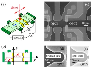
The first wafer, referred to as A in this paper, has a carrier density and mobility of the 2D electrons at liquid- helium temperature of about ns=7−8×1011cm−2and μ=1.5×106cm2/V s, respectively. This mobility corre- sponds to a mean free path of 30µm, which substantially exceeds the QPC size being of the order of 100 nm. The second wafer (B) has density ns=5−6×1011cm−2and a much lower mobility μ=4×105 cm2/V s (the cor- responding mean free path is about 4 µm). The gates are fabricated on the surface of the heterostructure using electron-beam lithography with a distance of about 90 nm between the gate and the 2DEG. Figures 1(a) and 1(b) show schematically quantum point contacts with a tradi- tional split gate and bridged gate placed on two parts of a Hall bar sample. Microphotographs of the gated parts of the sample are shown in Figs.1(c)–1(e). The bridged- gate QPC consists of a single piece of metal with a semielliptical narrowing, see Fig.1(d).
Samples are placed in an optical cryostat with z-cut crys- tal quartz windows. To exclude (inhibit) illumination of the sample with room, visible, or infrared light all win- dows are covered by a thick black polyethylene film, which is transparent in the terahertz range but blocks out visible and infrared light. We use an exchange gas cryostat, which allows us to measure the temperature dependence of the dark conductance. All experiments on the photoresponse
FIG. 1. (a),(b) Sketch of Hall bar samples with two QPC struc- tures obtained by gates placed on two parts of the sample. The size of the Hall bar is 280×20µm2, the length and width of the arms of the gates are 25 and 6µm, respectively. The dou- ble arrow indicates the electric field vector E(ω) of normally incident THz radiation. The orientation ofE(ω)with respect to the x axis is described by the azimuthal angle α, see (b). (c) Microphotograph of the gated part of the sample. (d),(e) Enlarged images of the bridged-gate QPC and a traditional split-gate QPC, respectively.
are performed on samples in a liquid-helium bath, i.e., at T=4.2 K.
The resistance R=1/G is measured using the electric circuit shown in Fig.1(a)and a conventional lock-in tech- nique with a frequency of 3 Hz and currents J =(10−10− 10−8) A. Figure2shows the gate-voltage dependence of the normalized dark conductance Gdark(Veffg )/G0 obtained for J =10−10 A. Here, G0=2e2/h is the conductance quantum. The data obtained for the nonilluminated struc- tures A and B reveal that at a temperature of T=4.2 K and in the used range of gate voltages, the conductance G(Vg) is much smaller than G0, i.e., all QPCs operate in the tunneling regime. Note that while the overall charac- teristics of the QPCs remain the same, values of the gate voltage corresponding to the conductance G0 depend on the cooldown procedure and differ from sample to sample.
This is ascribed to cooldown-dependent charge trapping in the insulator. To compare the measurements taken at dif- ferent sample cooldowns we plot the data as a function of the effective gate voltage Veffg =Vg−Vg(0.1G0) with Vg(0.1G0)being the gate voltage at which the conductance is equal to 0.1G0.
The regime of complete tunneling of a QPC, with the resistance up to several Mis realized for samples cooled below T≈10 K. This can be seen in the temperature dependence of the conductance shown for the bridged-gate QPC (made of wafer A) and the split-gate one (made of wafer B) in the inset in Fig.2. It is seen that the temper- ature dependencies are similar for both kinds of samples,
eff
dark 0 dark 0
FIG. 2. Dependence of the relative dark conduc- tance Gdark(Veffg )/G0 on the effective gate voltage Veffg =Vg−Vg(0.1G0). Here, the values of Vg correspond- ing to G=0.1G0 are −2.23 V (bridged-gate sample A),
−2.05 V (split-gate sample B), and−1.80 V (bridged-gate sam- ple B). The dependencies are measured at T=4.2 K. The inset shows the temperature dependencies obtained at Veffg = −78 mV for the bridged-gate sample A and Veffg = −61 mV for the split-gate sample B.
demonstrating exponential growth for T>15 K (with an activation temperature of about 60 K) and saturation of the conductance at low temperatures. The latter gives evi- dence for the tunneling regime in the latter case. From the value of the saturated conductance Gdark=7×10⁻⁴G0, we estimate the barrier height as about 5 and 4.5 meV for the bridged-gate sample A and the split-gate sample B, respectively. Note that in spite of the different parameters of the 2DEG and different QPC shapes, we obtain almost the same barrier heights for the same dark conductance.
B. Methods
To measure the terahertz photoconductance of the QPCs we use a THz gas laser [29,30] optically pumped by a CO2
laser [31]. Radiation with frequency f =0.69 and 1.63 THz (wavelengths ofλ=432 and 184µm) are obtained using CH2O2 and CH2F2 gases, respectively. The cor- responding photon energies ω are 2.85 and 6.74 meV, respectively. All experiments are performed at normal inci- dence of radiation, see Fig. 1(a), and a temperature of T=4.2 K. The radiation is focused onto a spot of about 2 mm diameter. The spatial beam distribution has an almost Gaussian profile, measured by a pyroelectric camera. The radiation intensity I on the QPC structures is about 50 and 200 mW/cm2 for f =0.69 and 1.63 THz, respec- tively. Room-temperature halfwave plates are placed just in front of the cryostat to rotate the polarization plane of the radiation by an azimuthal angleα. The quality of the
eff
darkph
FIG. 3. Dependencies of the relative terahertz photoconductiv- ity Gph/Gdarkon the effective gate voltage Veffg . Data are obtained for wafers A and B with different gate configurations by apply- ing radiation with f =0.69 THz and intensity I=50 mW/cm2. Solid curves show fits according to Gph/Gdark=A exp(−Veffg /a), where A and a are the fit parameters.
linear polarization at the sample position is controlled by independent measurements applying a grid polarizer and a polarization insensitive pyroelectric detector. The photore- sponse, similar to the transport experiments, is measured by applying the electric circuit shown in Fig. 1(a) for currents J =(10−9−10−8)A.
III. RESULTS
First, we discuss the results obtained at a radiation frequency f =0.69 THz with the electric field vector ori- ented along x direction, i.e., normally to the gate stripes.
Irradiating the structure with the THz beam at normal incidence, we detect a photoconductive signal correspond- ing to the conductivity increase [32–35], which drastically raises for large negative gate voltages, see Fig.3. The lat- ter corresponds to the dark conductance decrease, see Fig.
2. The figure reveals that at the lowest dark conductance the photoconductance exceeds the dark one by almost two orders of magnitude. Figure3also shows that the photo- conductive response Gph/Gdark is substantially larger for higher mobility samples, see data in Fig. 2 for bridged- gated samples A and B. Furthermore, its magnitude is larger for the bridged-gate QPC than for the split-gate structure. This difference has been previously observed in the microwave range on similar structures [14].
Exploiting the advantage of THz laser radiation, which, in contrast to radiation in the microwave-frequency range, allows accurate polarization experiments to be performed [36], we investigate the variation of the photoresponse as a function of the orientation of the radiation electric field
eff
G/ Gph dark eff
FIG. 4. Dependencies of the terahertz photoconductance Gph/G0 on the orientation of the terahertz radiation electric- field vector Efor bridged-gate samples A (blue triangles) and B (red circles). Data are obtained for the effective gate voltages Veffg = −51 mV (sample A) and−24 mV (sample B) correspond- ing to the values of Gdark/G0=0.0018 and 0.003, respectively.
The solid curve is a fit according to Gph/Gdark∝(cosα)2. The inset shows the orientation of the vectorEcorresponding to the signal maximum. Arrows on top illustrate the orientations of the radiation electric field vector for several values ofα.
vector. Figure 4 shows the dependence of the photocon- ductance Gph/Gdark on the azimuthal angle α measured for bridged-gate samples A and B. The figure reveals that the photoresponse can be well fitted by Gph/Gdark∝cos2α and achieves its maximum for a radiation electric field vector oriented perpendicular to the gate stripes (Ex).
Now, we turn to the photoresponse obtained for the higher radiation frequency. Increasing the frequency by about 2.5 times, we observe a drastic (by more than one order of magnitude) reduction of the photoconductance Gph/G0. This is shown in Fig. 5 for the bridged-gate samples A and B excited by radiation with frequencies f =0.69 and 1.63 THz. Furthermore, for higher frequen- cies, the photoresponse becomes almost independent on the effective gate voltage.
IV. DISCUSSION
The giant terahertz photoconductance of a tunneling point contact and its behavior upon variation of radiation polarization, frequency, and intensity can be well described by the model of coherent photon-assisted tunneling in QPCs developed in Ref. [15].
Let us first consider, at a qualitative level, the enhance- ment of the electric current in a QPC operating in the tunneling regime under the action of normally incident
Gph / GdarkGph / Gdark
eff
eff
FIG. 5. (a),(b) Dependencies of the photoconductance Gph/Gdark on the effective gate voltage Veffg measured for two radiation frequencies in bridged-gate samples A and B, respectively.
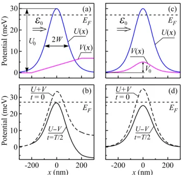
linearly polarized terahertz radiation. The effect of the radi- ation field is twofold: (i) It causes an additional force in the direction of the tunneling current due to the x compo- nent of the terahertz electric fieldE(ω)and (ii) it reduces the tunneling barrier due to the Ez(ω) component of the electric field originating from the near field of diffraction [18,37]. The model of the potential modification and the corresponding enhancement of tunneling is shown in Fig.
6. It is assumed that the QPC in the tunneling regime can be considered as a one-dimensional barrier U(x)= U0/cosh2(x/W)(blue solid curve), where U0is the barrier height and W is its characteristic width [3,15]. The Fermi energy EF =27 meV sketched by the dashed line in this figure is determined from the electron density ns=7.5× 1011 cm−2, which is obtained from transport measure- ments. Figures6(a)and6(b)illustrate the influence of the Ex-field component resulting in a force eE0,x(ω)cos(ωt)=
[dV(x)/dx] cos(ωt) applied along x direction shown in Fig.6(a) by the magenta line for one half of a period of the wave. The force results in a time-dependent potential U(x)+V(x)cos(ωt), which increases the tunneling cur- rent for one half of a period of the radiation field and decreases it for the other half. The corresponding potentials are shown in Fig.6(b)by solid and dashed curves. Obvi- ously the effect is maximal for the radiation polarized along the current, i.e., in x direction, as detected in our exper- iment. The second mechanism, considering the action of the potential U(x)=U0/cosh2(x/W), is illustrated in Figs.
6(c)and6(d). It is based on the reduction of the tunneling barrier U(x)due to the z component of the electric field. In the vicinity of the QPC formed by the spiked split gate and for a radiation electric field oriented along x direc- tion, i.e., normal to the gate stripes, near-field diffraction results in a field Ez directed along z direction for one half of a period and−z for the other. The corresponding time- dependent variation of the potential is shown in Fig.6(d) by solid and dashed curves. The reduction of the poten- tial barrier yields the increase of the tunneling current and, consequently, the conductance. For an electric field ori- ented along y direction, the Ez component becomes more complex and has opposite signs for opposite sides of the spiked gates forming the QPC and the effect vanishes.
Figure6and the above discussion present a semiclassi- cal description of the radiation-induced tunneling in QPCs, which illustrates the basic physics of the phenomena. This model, however, is valid only for rather low frequen- cies at which the characteristic time of electron tunneling through the potential barrier U(x)is smaller than 1/ω[38].
The crossover between low-frequency and high-frequency behavior occurs forωτ =1. Following Landauer and Büt- tiker [38], the tunneling time is estimated in the Wentzel- Kramers-Brillouin (WKB) limit as τ =(πW)√
m∗/2U0, where m∗=0.07me is the effective electron mass. For barrier parameters U0=30 meV and W=100 nm we obtainτ ≈0.8 ps. Then at frequencies f =0.69 and f = 1.63 THz the values of ωτ are 3.5 and 8.2, respectively.
Therefore, photon emission and absorption transitions are important in this frequency range, and one has to deal with the time-dependent Schrödinger equation.
For modeling the experimental photoresponse, we use the theory of photon-assisted transmission [39] adapted for QPC in the tunneling regime in Ref. [15]. In the framework of this model, the Schrödinger equation
i∂ ∂
t = − 2 2m∗
∂2
∂x2 +[U(x)+V(x)cos(ωt)] . (1) with the time-dependent potential U(x)+V(x)cos(ωt) is solved numerically.
The potentials U(x)and V(x)are assumed to be piece- wise constant functions (step approximation) as Coon and Liu suggested in Ref. [39]. This approximation extends
FIG. 6. Schematic drawings of the QPC potential barriers U(x) in the plane of the QPC and their modifications upon action of the radiation electric field given by U(x)+V(x)cos(ωt). (a) Elec- trostatic potential barrier in x direction (solid blue curve) and radiation electric force eE0,x(ω)cos(ωt)=[dV/dx] cos(ωt)act- ing on the electrons for one half of a period at|x|<2W (solid magenta line). (b) Modification of the potential barrier due to the Ex(ω)component of the radiation field is shown for two instants in time, t=0 and t=T/2, shifted by half a period. (c) Electro- static potential barrier in x direction and dynamic barrier with the height V0caused by the Ez(ω)component of the radiation elec- tric field. (d) Change of the potential U(x)+V(x)cos(ωt)due to the Ez(ω)component shown for two instants in time, t=0 and t=T/2, shifted by half a period.
the treatment of one-dimensional scattering in the high- frequency field by Tien and Gordon [27] and Landauer and Büttiker [38] to potentials of arbitrary shape. Elec- trons with energyE0 and a fixed amplitude are scattered on the region with nonuniform U(x) and V(x). Outside the region the potentials are constant functions. The elec- trons are transmitted and reflected into energy channels E0±nω with respective complex amplitudes. The mul- tichannel wave function is the sum of plain waves within the constancy intervals and the coefficients are determined by matching the wave functions at the boundaries of adja- cent intervals. For given boundary conditions at x→ ±∞, this technique yields all transmission and reflection ampli- tudes. In our modeling, the potentials U(x) and V(x) are approximated on a fine mesh with δx=1−10 nm inside the interval |x|<2W and constant values outside the interval (Fig. 6). The number of energy channels taken into the sum is dependent on model parameters and varied to attain acceptable accuracy. The conductance is found by the Landauer formula at zero temperature [40]:
G=G0D(E0), where D(E0)is the total multichannel trans- mission coefficient for an electron incident with energyE0. The barrier height, U0=30 meV (U0−EF =3 meV), is calculated from the dark conductance value after G= G0D with the tunneling transmission D=0.002 for the barrier shape U(x)=U0/cosh2(x/W), E0=27 meV and W=100 nm. Calculations using the above values show that the observed increase of the conductance by 50 times for a dark conductance G=0.002G0, frequency f =0.69 THz, and the highest radiation power used in our work corresponds to a variation of the barrier U0 by V0=5 meV. Thus for the radiation used in our experi- ments (f =0.69 THz,ω=2.85 meV) we obtain the ratio V0/ω≈2.
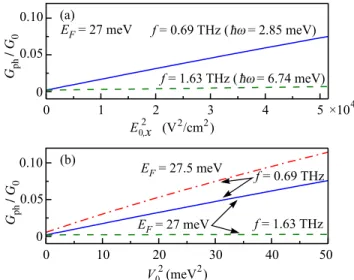
Figure 7 presents the results of calculations carried out in the framework of the above model. It shows the dependence of the conductance G/G0 on the square of the radiation electric field E0,x2 , (a), and the corresponding potential V20, (b), calculated for frequencies 0.69 and 1.63 THz. Here, the ratio of E0,x/V0is scaled such that the mag- nitudes of the conductance for f =0.69 THz at the highest V0 matches that at the highest E0,x field. Comparison of Figs.7(a)and (b) demonstrates that both mechanisms yield almost the same behavior of G(E0,x2 ), (a), and G(V20), (b).
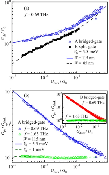
The calculated dependence describes the experimental one well as shown in the inset in Fig. 8(b) for the bridged- gate sample B. A good agreement is also obtained for the dependence of the normalized photoconductance Gph/G0
and Gph/Gdarkon the dark conductance Gdark/G0, see Fig.
8. We note that plotting Gph against Gdark allows exper- iment and modeling to be compared independently of the parameters of the 2DEG, the kind of structure, or the shape of gate. In particular, the calculations reveal a drastic sup- pression of the photoresponse both for the transition of the QPC from the tunneling to open regime and for the change of frequency in the tunneling regime from 0.69 to 1.63 THz. This is in full agreement with the experimental results, see Figs.5and8(b). The higher photoconductance for 0.69 THz (ω=2.85 meV) is explained by transitions to the channels E =E0±nω, n=0, 1. These channels belong to the tunneling mode and thus have classical turn- ing points with a high probability density of discovering the electron, whereas for 1.63 THz (ω=6.74 meV) the channel E0+ω already belongs to the open mode with larger delocalization, smaller probability density in the barrier, and, therefore, reduced transition efficiency.
Finally, we note that the fitting of the model to the experiment is mainly determined by two parameters—the characteristic width W of the QPC barrier and the inten- sity of irradiation described by V0 (or E0,x). The values for optimal fitting W=115 and 85 nm for bridged-gate and split-gate samples are close to the lithographic size of the gates. The amplitude of the high-frequency potential V0=5.5 meV corresponds to the extreme value dV(x)/
edx=423 V/cm or E0,x =176 V/cm, which is almost 70 Gph / G0Gph / G0
FIG. 7. Calculated power dependencies of the photoconduc- tance in a tunneling QPC in response to terahertz radiation of two frequencies. (a),(b) Dependencies on the magnitude of the radiation electric field strength E20,xand dynamic barrier ampli- tude V20, respectively. Calculations are carried out using T=0 K, EF =27 meV, U0=30 meV, and W=85 nm. (b) The result of calculations for f =0.69 THz and a slightly larger Fermi energy EF =27.5 meV (red dotted-dashed line).
or 30 times larger than the maximum value calculated for the incoming plane wave (E0=6.14 V/cm at the radia- tion intensity I =50 mW/cm2). This observation agrees with previous studies relying on the near field of diffrac- tion for which a strong enhancement of the field amplitude in the vicinity of a metal edge (in our case the spiked gates forming the QPC) has been reported [18,41,42].
V. POSSIBLE ROLE OF THE ELECTRON GAS HEATING
Finally, we discuss the possible role of electron gas heating in the observed phenomena. First, we address the effect of the electron temperature increase. A substantial contribution of this mechanism can be ruled out based on the polarization dependence of the photoconductivity and on estimations of the electron temperature provided by independent measurements on the macroscopic part of the sample. A strong variation of the photoresponse with rotation of the radiation electric field vectorE, see Fig.4, indicates that the tunneling current across the QPC has a maximum forEoriented parallel to the current (α=0) and vanishes forα=90◦. For the electron gas heating mecha- nism, however, the increase of the tunneling probability is caused by the rise of the 2DEG temperature due to Drude- like radiation absorption and any polarization dependence is not expected. Furthermore, the polarization dependence cannot be explained as a variation of the radiation cou- pling to the 2DEG by a dipole antenna formed by the metal gate bars, because in this case the maximum current
Gph / G0Gph / Gdark Gph / Gdark
Gdark / G0
Gdark / G0
Gdark / G0
FIG. 8. Theoretical and experimental dependencies of (a) Gph/G0and (b) Gph/Gdarkon the normalized dark conductivity Gdark/G0. The data in (a) are shown for bridged-gate sample A and split-gate sample B excited by radiation with f =0.69 THz and intensity I=50 mW/cm2. Calculated curves are obtained with U0=30 meV, V0=5.5 meV, W=115 nm (sample A), and 85 nm (sample B). The data in (b) are presented for bridged- gate sample A excited by radiation frequencies f =0.69 and 1.63 THz (intensity I=50 mW/cm2). Curves are calculated using U0=30 meV, W=115 nm, and potentials V0=5.5 meV (f =0.69 THz) and 1 meV (f =1.63 THz). The inset shows dependencies for the bridged-gate sample B.
would be expected forE parallel to the gate stripes, i.e., α=90◦. This, however, contradicts the experiment where the photoresponse has a maximum for E oriented paral- lel to the current (α=0) and is vanishingly small forα= 90◦, see Fig. 4. Moreover, electron-heating-based expla- nations applying Drude-like radiation absorption would result in substantially weaker reduction of the photore- sponse. Instead of the observed photoresponse decrease by 50 times in the experiment due to the frequency increase from 0.69 to 1.63 THz, see Fig.5, the Drude absorption,
scaling as 1/[1+(ωτ)2], will yield a signal decrease by a factor of 7 only.
The conclusion that an increase of the electron tempera- ture does not play a substantial role in the photoconductive response is also supported by the estimation of the effect of electron gas heating. For that we perform measurements on a macroscopic part of the sample which does not contain the QPC structure. Comparing the temperature dependence of the conductivity with and without continuous-wave THz radiation (not shown), we observe that at the highest power level used in this work the 2DEG temperature increases only by T≈1 K or even less [43]. This increase of the electron temperature is not sufficient to explain the observed increase by one to two orders of magnitude, see Fig.3.
While the increase of the electron temperature in the 2DEG seems unlikely to be responsible for the observed signal, the mechanism based on the influence of terahertz radiation on the steady-state electron-distribution function near the tunnel contact considered in [14] for microwave frequencies is not excluded by the above arguments. This mechanism should be enhanced for the radiation electric- field vector oriented along x direction, as observed in the experiment, and does not rely on the electron temperature.
At the same time, the magnitude of the photoconductivity in this case is also proportional to the Drude absorption, which is characterized by a weaker frequency dependence as that detected in our experiments, see the above discus- sion and Fig. 5. Thus, the theory of Ref. [14] yielding a good agreement for microwave frequencies does not explain a strong frequency dependence of the terahertz- radiation-induced photoconductivity in the QPC structure.
VI. SUMMARY
To summarize, we observe a giant terahertz photocon- ductive response of the QPC operating in the tunneling regime. Experimental findings are in good agreement with the theory of the photon-assisted transmission [39] as applied to tunneling in QPC [15]. The observed change in conductivity by more than two orders of magnitude in response to rather weak terahertz radiation demonstrates that QPCs in the tunneling regime can be considered as a good candidate for detection of terahertz and microwave [14] radiation. Our results show that they would have com- parable noise equivalent power per unit band (NEP*) with the composite Si bolometer, InSb hot electron bolometer, and GaAs photodetectors [44], do not require antennas and, being produced by planar technology, can be com- bined in a matrix. The latter is of particular importance because it is easy in fabrication, can be well integrated in external circuits, has a small size, can be used for imag- ing and should have a high sensitivity and low NEP*.
Note that the QPCs discussed above are not optimized for detection purposes. As for the future work, the most
challenging task is the search for the steplike frequency or gate-voltage dependence of the photoconductive response.
Preliminary calculations for the deep tunneling regime of the QPC show shoulderlike features in the gate-voltage dependence of the photoconductance and peaks and dips in the frequency dependence.
ACKNOWLEDGMENTS
S.D.G. thanks S. Mikhailov and V. Popov for fruitful discussions. O.A.T. and V.A.T. are grateful to D.G. Bak- sheev for assistance in modeling. The financial support of this work by German Science Foundation (DFG) (Grant No. SFB 1277, project A04), RFBR (Grants No. N 17-02- 00384 and N 16-38-00851), and the Volkswagen Stiftung Program is acknowledged.
[1] B. J. van Wees, H. van Houten, C. W. J. Beenakker, J. G.
Williamson, L. P. Kouwenhoven, D. van der Marel, and C.
T. Foxon, Quantized Conductance of Point Contacts in a Two-dimensional Electron Gas,Phys. Rev. Lett. 60, 848 (1988).
[2] D. Wharam, T. J. Thornton, R. Newbury, M. Pepper, H.
Ahmed, J. E. F. Frost, D. G. Hasko, D. C. Peacock, D. A.
Ritchie, and G. A. C. Jones, One-dimensional transport and the quantisation of the ballistic resistance,J. Phys. C: Solid State Phys. 21, L209 (1988).
[3] M. Büttiker, Quantized transmission of a saddle-point con- striction,Phys. Rev. B 41, 7906 (1990).
[4] H. van Houten and C. W. J. Beenakker, Quantum point contacts,Phys. Today 49, 22 (1996).
[5] P. S. Dorozhkin, S. V. Tovstonog, S. A. Mikhailov, I.
V. Kukushkin, J. H. Smet, and K. von Klitzing, Reso- nant detection of microwave radiation in a circular two- dimensional electron system with quantum point contacts, Appl. Phys. Lett. 87, 092107 (2005).
[6] J. W. Song, G. R. Aizin, J. Mikalopas, Y. Kawano, K. Ishibashi, N. Aoki, J. L. Reno, Y. Ochiai, and J.
P. Bird, Bolometric terahertz detection in pinched-off quantum point contacts, Appl. Phys. Lett. 97, 083109 (2010).
[7] R. A. Wyss, C. C. Eugster, J. A. del Alamo, and Q. Hu, Far- infrared photon-induced current in a quantum point contact, Appl. Phys. Lett. 63, 1522 (1993).
[8] C. Karadi, S. Jauhar, L. P. Kouwenhoven, K. Wald, J. Oren- stein, P. L. McEuen, Y. Nagamune, and H. Sakaki, Dynamic response of a quantum point contact,J. Opt. Soc. Am. B 11, 2566 (1994).
[9] J. W. Song, N. A. Kabir, Y. Kawano, K. Ishibashi, G. R.
Aizin, L. Mourokh, J. L. Reno, A. G. Merkelz, and J. P.
Bird, Terahertz response of quantum point contacts,Appl.
Phys. Lett. 92, 223115 (2008).
[10] T. J. Janssen, J. C. Maan, J. Singleton, N. K. Patel, M.
Pepper, J. E. Frost, D. A. Ritchie, and G. A. C. Jones, A new mechanism for high-frequency rectification in a bal- listic quantum point contact,J. Phys.: Condens. Matter 6, L163 (1994).
[11] Q. Hu, Photon-assisted quantum transport in quantum point contacts,Appl. Phys. Lett. 62, 837 (1993).
[12] R. A. Wyss, C. C. Eugster, J. A. del Alamo, and Q. Hu, Far- infrared photon-induced current in a quantum point contact, Appl. Phys. Lett. 63, 1522 (1993).
[13] R. A. Wyss, C. C. Eugster, J. A. del Alamo, Q. Hu, M. J.
Rooks, and M. R. Melloch, Far-infrared radiation-induced thermopower in a quantum point contact,Appl. Phys. Lett.
66, 1144 (1995).
[14] A. D. Levin, G. M. Gusev, Z. D. Kvon, A. K. Bakarov, N.
A. Savostianova, S. A. Mikhailov, E. E. Rodyakina, and A. V. Latyshev, Giant microwave photo-conductance of a tunnel point contact with a bridged gate,Appl. Phys. Lett.
107, 072112 (2015).
[15] O. A. Tkachenko, V. A. Tkachenko, and Z. D. Kvon, Photon-assisted electron transport through a quantum point contact in a microwave field, JETP Lett. 102, 378 (2016).
[16] P. S. S. Guimar aes, B. J. Keay, J. P. Kaminski, S. J. Allen, Jr., P. F. Hopkins, A. C. Gossard, L. T. Florez, and J. P. Har- bison, Photon-mediated Sequential Resonant Tunneling in Intense Terahertz Electric Fields,Phys. Rev. Lett. 70, 3792 (1993).
[17] B. J. Keay, S. J. Allen, Jr., J. Galán, J. P. Kaminski, J.
L. Campman, A. C. Gossard, U. Bhattacharya, and M. J.
W. Rodwell, Photon-assisted Electric Field Domains and Multiphoton-assisted Tunneling in Semiconductor Super- lattices,Phys. Rev. Lett. 75, 4098 (1995).
[18] S. D. Ganichev and W. Prettl, Intense Terahertz Excita- tion of Semiconductors (Oxford University Press, Oxford, 2006), pp. 93–130 and 145–161.
[19] V. A. Chitta, R. E. M. de Bekker, J. C. Maan, S. J.
Hawksworth, J. M. Chamberlain, M. Henini, and G. Hill, Photon-assisted tunneling in sequential resonant tunneling devices,Semicond. Sci. Technol. 7, 432 (1992).
[20] H. Drexler, J. S. Scott, S. J. Allen, K. L. Campman, and A.
C. Gossard, Photon-assisted tunneling in a resonant tunnel- ing diode: Stimulated emission and absorption in the THz range,Appl. Phys. Lett. 67, 2816 (1995).
[21] J. Faist, F. Capasso, C. Sirtori, D. Sivco, and A. Cho, Inter- subband Transitions in Quantum Wells: Physics and Device Applications II (Academic, San Diego, 2000), pp. 2–83 and 127–186.
[22] L. P. Kouwenhoven, S. Jauhar, J. Orenstein, P. L. McEuen, Y. Nagamune, J. Motohisa, and H. Sakaki, Observation of Photon-assisted Tunneling Through a Quantum Dot,Phys.
Rev. Lett. 73, 3443 (1994).
[23] S. D. Ganichev, W. Prettl, and P. G. Huggard, Phonon Assisted Tunnel Ionization of Deep Impurities in the Elec- tric Field of Far-infrared Radiation,Phys. Rev. Lett. 71, 3882 (1993).
[24] S. D. Ganichev, E. Ziemann, Th. Gleim, W. Prettl, I. N.
Yassievich, V. I. Perel’, I. Wilke, and E. E. Haller, Carrier Tunneling in High-frequency Electric Fields, Phys. Rev.
Lett. 80, 2409 (1998).
[25] S. D. Ganichev, Tunnel ionization of deep impurities in semiconductors induced by terahertz electric fields,Physica B 273-274, 737 (1999).
[26] A. H. Dayem and R. J. Martin, Quantum Interaction of Microwave Radiation with Tunneling between Supercon- ductors,Phys. Rev. Lett. 8, 246 (1962).
[27] P. K. Tien and J. P. Gordon, Multiphoton process observed in the interaction of microwave fields with the tunnel- ing between superconductor films, Phys. Rev. 129, 647 (1963).
[28] S. Shapiro, Josephson Currents in Superconducting Tun- neling: The Effect of Microwaves and Other Observations, Phys. Rev. Lett. 11, 80 (1963).
[29] Z. D. Kvon, S. N. Danilov, N. N. Mikhailov, S.
A. Dvoretsky, and S. D. Ganichev, Cyclotron res- onance photoconductivity of a two-dimensional elec- tron gas in HgTe quantum wells, Physica E 40, 1885 (2008).
[30] S. D. Ganichev, S. A. Tarasenko, V. V. Bel’kov, P. Olbrich, W. Eder, D. R. Yakovlev, V. Kolkovsky, W. Zaleszczyk, G. Karczewski, T. Wojtowicz, and D. Weiss, Spin Currents in Diluted Magnetic Semiconductors,Phys. Rev. Lett. 102, 156602 (2009).
[31] C. Jiang, V. A. Shalygin, V. Y. Panevin, S. N. Danilov, M. M. Glazov, R. Yakimova, S. Lara-Avila, S. Kubatkin, and S. D. Ganichev, Helicity-dependent Photocurrents in Graphene Layers Excited by Midinfrared Radiation of a CO2Laser,Phys. Rev. B 84, 125429 (2011).
[32] Note that the photoresponse is caused by the change of the conductivity only: Neither photon drag nor photogalvanic contributions are detected. This is in agreement with the phenomenological theory of these photocurrents which, for 2DEG structures grown on (001)-oriented surfaces excited at normal incidence, are forbidden by symmetry arguments excluding photocurrents [33–35].
[33] S. D. Ganichev, E. L. Ivchenko, and W. Prettl, Photo- galvanic effects in quantum wells, Physica E 14, 166 (2002).
[34] V. V. Bel’kov, S. D. Ganichev, Petra Schneider, C. Back, M. Oestreich, J. Rudolph, D. Hägele, L. E. Golub, W.
Wegscheider, and W. Prettl, Circular photogalvanic effect at inter-band excitation in semiconductor quantum wells, Solid State Commun. 128, 283 (2003).
[35] P. Schneider, J. Kainz, S. D. Ganichev, V. V. Bel’kov, S.
N. Danilov, M. M. Glazov, L. E. Golub, U. Rössler, W.
Wegscheider, D. Weiss, D. Schuh, and W. Prettl, Spin relax-
ation times of 2D holes from spin sensitive bleaching of inter-subband absorption,J. Appl. Phys. 96, 420 (2004).
[36] T. Herrmann, I. A. Dmitriev, D. A. Kozlov, M. Schnei- der, B. Jentzsch, Z. D. Kvon, P. Olbrich, V. V. Bel’kov, A.
Bayer, D. Schuh, D. Bougeard, T. Kuczmik, M. Oltscher, D.
Weiss, and S. D. Ganichev, Analog of microwave-induced resistance oscillations induced in GaAs heterostructures by terahertz radiation,Phys. Rev. B 94, 081301(R) (2016).
[37] V. V. Klimov and V. S. Letokhov, A simple theory of the near field in diffraction by a round aperture,Optics Comm.
106, 151 (1994).
[38] M. Büttiker and R. Landauer, Traversal Time for Tunnel- ing,Phys. Rev. Lett. 49, 1739 (1982).
[39] D. D. Coon and H. C. Liu, Time-dependent quantum-well and finite-superlattice tunneling, J. Appl. Phys. 58, 2230 (1985).
[40] Experiment shows that at a fixed Vg the dark conductance does not depend on temperature in the region T<10 K (see the inset of Fig. 2). Therefore, we perform all the calculations for T=0.
[41] P. Olbrich, J. Kamann, M. König, J. Munzert, L. Tutsch, J.
Eroms, D. Weiss, M.-H. Liu, L. E. Golub, E. L. Ivchenko, V. V. Popov, D. V. Fateev, K. V. Mashinsky, F. Fromm, Th. Seyller, and S. D. Ganichev, Terahertz ratchet effects in graphene with a lateral superlattice, Phys. Rev. B 93, 075422 (2016).
[42] P. Faltermeier, G. V. Budkin, J. Unverzagt, S. Hubmann, A. Pfaller, V. V. Bel’kov, L. E. Golub, E. L. Ivchenko, Z.
Adamus, G. Karczewski, T. Wojtowicz, V. V. Popov, D.
V. Fateev, D. A. Kozlov, D. Weiss, and S. D. Ganichev, Magnetic quantum ratchet effect in (Cd,Mn)Te- and CdTe- based quantum well structures with a lateral asymmetric superlattice,Phys. Rev. B 95, 155442 (2017).
[43] Note that even if near-field effects better couple the radia- tion to the electron gas in the vicinity of metal bars as in the 2DEG “bulk,” the efficient electron-electron scattering results in a fast redistribution of the absorbed energy in the whole ensemble of 2D electrons.
[44] E. Bründermann, H.-W. Hübers, and M. Kimmitt, Terahertz Technique (Springer, Berlin Heidelberg, 2012).