Photophysical Characterizations of OLED Relevant Cu(I) Complexes Exhibiting Thermally Activated
Delayed Fluorescence (TADF)
Dissertation
zur Erlangung des Doktorgrades der Naturwissenschaften (Dr. rer. nat.) an der Fakult¨ at f¨ ur Chemie und Pharmazie
der Universit¨ at Regensburg
vorgelegt von Markus J. Leitl
aus Winzer
2015
Promotionsgesuch eingereicht am: 22. Januar 2015 Tag der m¨undlichen Pr¨ufung: 9. M¨arz 2015
Die Arbeit wurde angeleitet von Prof. Dr. Hartmut Yersin am Institut f¨ur Physikalische und Theoretische Chemie der Universit¨at Regensburg.
Pr¨ufungsausschuss: Prof. Dr. Werner Kunz, Vorsitzender
Prof. Dr. Hartmut Yersin, Erster Gutachter Prof. Dr. Bernhard Dick, Zweiter Gutachter Prof. Dr. Alfons Penzkofer
Parts of this thesis have been published previously
Markus J. Leitl, Valentina A. Krylova, Peter I. Djurovich, Mark E. Thompson, Hart- mut Yersin
Phosphorescence versus Thermally Activated Delayed Fluorescence. Controlling Singlet- Triplet Splitting in Brightly Emitting and Sublimable Cu(I)-Compounds
Journal of the American Chemical Society 2014, 136, 16032.
Hartmut Yersin, Markus J. Leitl, Rafa l Czerwieniec
TADF for Singlet Harvesting – Next Generation OLED Materials Based on Brightly Green and Blue Emitting Cu(I) and Ag(I) Compounds
Proceedings of the SPIE 2014, 9183, 91830N-1.
Charlotte L. Linfoot, Markus J. Leitl, Patricia Richardson, Andreas F. Rausch, Oleg Chepelin, Fraser J. White, Hartmut Yersin, Neil Robertson
Selected as cover article
Thermally Activated Delayed Fluorescence (TADF) and Enhancing Photoluminescence Quantum Yields of [CuI(diimine)(diphosphine)]+ Complexes – Photophysical, Structural, and Computational Studies
Inorganic Chemistry 2014, 53, 10854.
Markus J. Leitl, Fritz-Robert K¨uchle, Hermann A. Mayer, Lars Wesemann, Hartmut Yersin
Brightly Blue and Green Emitting Cu(I) Dimers for Singlet Harvesting in OLEDs The Journal of Physical Chemistry A 2013, 117, 11823.
Further publications
Daniel A. Kunz, Markus J. Leitl, Lukas Schade, Jasmin Schmid, Beate Bojer, Ulrich T. Schwarz, Geoffrey A. Ozin, Hartmut Yersin, Josef Breu
Quasi-Epitaxial Growth of [Ru(bpy)3]2+ by Confinement in Clay Nanoplatelets Yields Polarized Emission
Small 2015, 11, 792.
Matthias St¨oter, Bernhard Biersack, Sabine Rosenfeldt,Markus J. Leitl, Hussein Kalo, Rainer Schobert, Hartmut Yersin, Stefan F¨orster, Josef Breu
Encapsulation of Functional Organic Compounds in Nanoglass for Optically Anisotropic Coatings
Angewandte Chemie International Edition 2015, DOI: 10.1002/anie.201411137.
Matthias St¨oter, Bernhard Biersack, Sabine Rosenfeldt,Markus J. Leitl, Hussein Kalo, Rainer Schobert, Hartmut Yersin, Stefan F¨orster, Josef Breu
Nanoglas-Verkapselung funktionaler organischer Verbindungen f¨ur optisch anisotrope Beschichtungen
Angewandte Chemie 2015, DOI: 10.1002/ange.201411137.
Timo Gneuß, Markus J. Leitl, Lars H. Finger, Nicholas Rau, Hartmut Yersin, J¨org Sundermeyer
A New Class of Luminescent Cu(I) Complexes with Tripodal Ligands – TADF Emitters for the Yellow to Red Color Range
Dalton Transactions2015, DOI: 10.1039/C4DT02631D.
Alberto Bossi, Andreas F. Rausch, Markus J. Leitl, Rafa l Czerwieniec, Matthew T.
Whited, Peter I. Djurovich, Hartmut Yersin, Mark E. Thompson
Photophysical Properties of Cyclometalated Pt(II) Complexes: Counterintuitive Blue Shift in Emission with an Expanded Ligand π System
Inorganic Chemistry 2013, 52, 12403.
Sebastian Maderlehner, Markus J. Leitl, Hartmut Yersin, Arno Pfitzner
Halocuprates(I) with DABCO Cations – Syntheses and Photophysical Characterizations in preparation.
Rafa l Czerwieniec, Markus J. Leitl, Thomas Hofbeck, Robert Meier, Hartmut Yersin Unprecedently Long-Lived Phosphorescence of Cu(I) Complexes
in preparation.
Filed patents
Timo Gneuß,Markus J. Leitl, J¨org Sundermeyer, Hartmut Yersin
Kupfer(I)- und Silber(I)-Verbindungen mit Tripod Liganden f¨ur verbessertes Singulett- Harvesting durch kombinierte Singulett- und Triplett-Emission f¨ur OLEDs und andere optoelektronische Vorrichtungen
filed 2014.
Rafa l Czerwieniec, Thomas Hofbeck, Markus J. Leitl, Uwe Monkowius, Hartmut Yersin Erweitertes Singulett-Harvesting f¨ur OLEDs und andere optoelektronische Vorrichtungen DE102013106426A1, WO2014202675A1, filed 2013.
Rafa l Czerwieniec, Markus J. Leitl, Hartmut Yersin Optische Sauerstoff-Sensoren mit Kupfer(I)-Komplexen
DE102012101067A1, WO2013117460A2, WO2013117460A3, filed 2012.
Fritz-Robert K¨uchle, Markus J. Leitl, Hermann A. Mayer, Lars Wesemann, Sophie Wernitz, Hartmut Yersin
Komplexverbindungen mit einem Liganden mit einem N- und einem P-Donor und ihre Verwendung im opto-elektronischen Bereich
DE201110079856A1, EP2737557A1, WO2013014066A1, filed 2011.
Contents
Motivation 11
1 Introduction to Organic Light Emitting Diodes 15
1.1 Electroluminescence . . . 15
1.2 Device Structure and Principle of Operation . . . 16
1.3 Triplet Harvesting and Singlet Harvesting . . . 20
2 Photophysical Properties of Transition Metal Complexes 27 2.1 Electronic States . . . 27
2.2 Spin-Orbit Coupling . . . 30
2.3 Temperature Dependence of Emission . . . 32
3 Dinuclear Copper Complexes 35 3.1 Complexes with Aminophosphine Ligands . . . 36
3.1.1 Crystal Structures . . . 36
3.1.2 Computational Investigations . . . 39
3.1.3 Spectroscopic Introduction . . . 41
3.1.4 Thermally Activated Delayed Fluorescence . . . 46
3.1.5 The Triplet State T1 . . . 50
3.1.6 Concluding Remarks . . . 56
3.2 Complexes with Diphosphine Ligands . . . 58
3.2.1 DFT and TDDFT Calculations . . . 58
3.2.2 Spectroscopic Discussion . . . 60
3.2.3 Comparative Discussion and Conclusion . . . 63
10
4 Mononuclear Copper Complexes 69
4.1 Cu(I) Complexes with two Bidentate Ligands . . . 69
4.1.1 Spectroscopic Discussion . . . 70
4.1.2 Temperature Dependent Measurements . . . 77
4.1.3 Conclusion . . . 79
4.2 Cu(I) Complexes with Three Coordinations . . . 81
4.2.1 Ambient Temperature Phosphorescence versus TADF . . . 81
4.2.2 Compound 2 – Typical Triplet Emitter . . . 84
4.2.3 Compound 1 – Thermally Activated Delayed Fluorescence . . . . 86
4.2.4 Controlling TADF by Ligand Orientation . . . 88
4.2.5 Conclusion . . . 93
Experimental Section 97
Summary 99
Conclusion 105
Bibliography 107
Motivation
For a long time, the more than hundred years ago developed light bulb has been the most widely spread artificial light source. This could change in the near future.
Organic light-emitting diodes (OLEDs) represent a new technology for the generation of light which is highly attractive for the use in displays as well as for illumination purposes.1,2 In the display sector, the application of this new technology offers clear advantages compared to state of the art liquid crystal displays (LCDs), for example, drastically higher in picture contrast, vast independence of the viewing angle, low energy consumption, and orders of magnitudes faster image refreshing rates. Furthermore, the OLED technology allows the realization of extremely thin and in addition flexible displays which opens up completely new perspectives for the design of respective devices. All these factors render OLEDs highly attractive and resulted in the fact that more and more cell phones with displays based on this technology are commercially available nowadays.
OLEDs are also assigned to possess a huge market potential in the lighting sector.
However, respective products do not qualify for mass production as of yet. In Ger- many, this issue has been addressed by large scale research projects initiated by the
“Bundesministerium f¨ur Bildung und Forschung” (German Ministry of Education and Research), for example by funding programs like “Organische Elektronik – Grundlagen der Technologie und Anwendungsszenarien” (Organic Electronics – Principles of the Technology and Scenarios for Applications).3 Such research initiatives are intended to help OLEDs entering the lighting market. In this regard, the launch of pilot production lines for OLEDs for illumination purposes, one of them being located at the OSRAM OLED GmbH in Regensburg, can be seen as a big step towards this direction.4
12 Motivation Of particular importance for the emission and performance properties of an OLED is the emitter material used which, after the injection of electrical charges, is stimulated to emit light. It turned out that third row transition metal complexes are particularly well suited for this purpose.1 In contrast to conventional fluorescent, purely organic compounds, these complexes exhibit a pronounced phosphorescence from their lowest excited triplet state with high emission quantum yields and short emission decay times.1,5–7 The underlying mechanism for this is the efficient coupling of spin and orbital angular momentum induced by the central metal ion. Furthermore and most importantly, the application of phosphorescent compared to conventional fluorescent emitters results in a four times higher OLED device performance as phosphorescent materials can show the triplet harvesting effect.1,8–10 This mechanism allows utilizing all electrically injected excitons, singlets and triplets, for the generation of light. For this reason, phosphorescent materials are strongly preferred to conventional fluorescent ones.
At the moment, triplet emitters based on the elements iridium and platinum are of particular relevance for commercial applications. However, this material class exhibits several disadvantages. On the one hand, iridium and platinum are noble metals that are extremely rare and therefore, emitters based on these materials are very cost intensive.
This fact would render the introduction of a wide spread OLED based illumination uneconomic. On the other hand, there are problems with the photophysical properties of this material class. For example, despite intense research efforts during the last two decades the development of long-term stable and efficient emitters for the blue color range still remains a major challenge.11,12
Although copper complexes are significantly more attractive due to the drastically lower costs,13 at first sight, they do not seem to be a viable alternative to the more expensive noble metal compounds. As copper possesses a considerably smaller spin orbit coupling constant compared to the distinctly heavier elements iridium and platinum it is expected that the phosphorescence decay times are significantly longer.5,6 This would result in pronounced saturation effects and as a consequence in significant efficiency losses when applied in electroluminescent devices. However, if the ligands are properly chosen, copper complexes can exhibit a very small energy separation ∆E(S1−T1) between the first excited singlet S1 and triplet T1 state. Therefore, at ambient temperature a thermal population of the singlet state S1 from the energetically lower lying triplet state T1 can occur. This mechanism opens an additional, highly effective radiative decay path to the S0 ground state and represents a thermally activated delayed fluorescence (TADF).5,6
13 Furthermore, as the emission in this case mainly occurs via the singlet state S1, a drastic reduction of the emission decay time is observed at ambient temperature. Importantly, emitters that exhibit a TADF also show the Singlet Harvesting effect.5,6 Accordingly, when applied in OLEDs the same high efficiencies can be achieved with them as with materials exhibiting the Triplet Harvesting effect.
The attractiveness of TADF compounds for electroluminescence applications has stimulated the development of new Cu(I) based emitter materials in recent years. However, it still remains a challenge to understand the correlations between chemical structure and emission properties and therefore, to specifically develop new materials with improved luminescence properties like higher emission quantum yields and shorter emission decay times. Gaining deeper insights into these structure-property relationships and developing a more detailed understanding for the photophysical processes of Cu(I) complexes represents the motivation for this thesis.
After a brief introduction to the basic concept of electroluminescence in chapter 1, a general overview over the electronic structure of transition metal compounds is given in chapter 2. The main part of this thesis, however, focuses on the investigation of different classes of Cu(I) complexes with spectroscopic and also with computational methods. In chapter 3, the discussion hereby centers around Cu(I) complexes containing two metal ions. In the first section of this chapter complexes in which an aminophosphine ligand is coordinated to each copper center and where the two copper centers themselves are bridged by two halides are studied. This allows a detailed examination of the influence of the halide on the emission properties. In the second part, the investigations are extended to a dinuclear Cu(I) compound with diphosphine ligands and its respective Ag(I) homologue and therefore gives insight how varying the chelating ligands and the central metal ions affects the electronic structure of these complexes. In chapter 4, Cu(I) compounds with one metal center are examined. In the first part, a pair of two tetrahedrally coordinated complexes is spectroscopically characterized. It is demonstrated how a slight chemical substitution can drastically increase the emission quantum yield. In addition, the effects of the surrounding matrix environment on the emission behavior are studied in detail. The second part focuses on the investigation of two structurally related three coordinated Cu(I) compounds, one of them showing a highly effective thermally activated delayed fluorescence, the other one showing intense phosphorescence at ambient temperature. This distinct difference in the emission behavior is rationalized by applying spectroscopic and computational methods. The thesis closes with a conclusion.
1
Introduction to Organic Light Emitting Diodes
1.1 Electroluminescence
The working principle of organic light emitting diodes (OLEDs) is based on the phe- nomenon of electroluminescence (EL), that is the generation of light by the application of an electrical field to the sample under investigation.14–16 Fundamental research in this field goes back to the first half of the 20th century. For the first time, electroluminescence was reported by Destriau when he investigated a powder sample of zinc sulfide which however was spoiled – nowadays this would be called doped – with copper.17 For organic compounds the observation of EL has been described by Bernanose et al. for the first time in 1953.18,19 In contrast to these two experiments, in which an alternating current voltage was required for the observation of EL, Pope et al. described luminescence from an anthracene single-crystal under application of a direct current voltage of several hundred Volts in 1963.20 However, the experiments of Destriau, Bernanose, and Pope required high driving voltages which limited EL to a laboratory environment. As a consequence, EL was of very limited relevance for technological applications. In the following years the driving voltages could be significantly reduced to well below 100 V.
This was achieved by shrinking the thickness of the devices to only a couple of 100 nm through the use of vacuum deposition in the production process. But also these devices did not become technologically relevant due to extremely short device lifetimes of only a couple of minutes which was mainly owed to the still relatively large voltages needed for operation.21 A major breakthrough could be achieved by Tang and van Slyke in 1987 by reducing the voltage necessary for operation to less than 10 V.22 This was possible by using a layered device structure in their experiments. More specifically, they applied
16 1 Introduction to Organic Light Emitting Diodes
Figure 1.1: Schematic representation of a three-layer OLED stack.
two different materials for the transport of electrons and holes from the cathode and anode, respectively, through the device to the recombination zone. On the one hand, this allowed an efficient injection and transport of the charge carriers without significant ohmic losses. On the other hand, in this way the recombination zone of electrons and holes could be limited to a narrow area on the interface of the two transport layers. This approach resulted in an at this time highly efficient device with an external emission quantum yield of about 1 %. In fact, this device structure laid the foundation for further developments and represented the starting point for extensive research in the field of organic light emitting diodes.
1.2 Device Structure and Principle of Operation
In general, an OLED can be even simpler than the two layer device suggested by Tang and van Slyke as in principle it is sufficient to sandwich one organic emissive layer between the anode and the cathode. In contrast to multilayer stacks though, such an approach suffers from inferior device performance, especially, regarding the device efficiency and lifetime.2,7,23,24 As the most simple device design that is of practical relevance a three layer stack can be considered. Figure 1.1 shows the structure of a such a device. In the following, the purpose of the individual components will be explained briefly.
The core component of every OLED is the emissive layer where the light emitting molecules are located. In the case of a small molecule OLED it consists of a hole and electron conducting matrix material into which the desired emitter is doped. Emitter ma-
1.2 Device Structure and Principle of Operation 17 terials that exhibit phosphorescence or thermally activated delayed fluorescence (TADF) are preferred as they can exhibit a four times larger electroluminescence emission quantum yield and therefore a four times larger device efficiency compared to conventional purely fluorescent emitters (compare section 1.3).1,2,6–8,23,24 At the moment, iridium(III)- and platinum(II)-complexes represent the most efficient class of phosphorescent emitters25–27 whereas copper(I)-complexes are entering the field of TADF emitters.13,28–43 Indepen- dently, recently also the potential of purely organic compounds that exhibit a TADF was recognized for the use in OLEDs.5,44–48 An interesting aspect is the emitter concentration in the emissive layer. Usually, large emitter concentrations are desired to realize OLEDs with high brightness. However, for iridium complexes and most other emitters it has been shown that an increase of the emitter concentration results in a decrease of the emission quantum yield due to intermolecular interactions such as triplet-triplet annihilation.49–51 Therefore, the doping concentration of the emissive layer is typically limited to the range between 5 % and 15 %. In contrast to this, copper compounds frequently do not exhibit such a self-quenching effect6,13,33,35,36 and could therefore be applied in much higher doping concentrations even up to 100 %.13,52,53
The emissive layer is sandwiched between two layers which are intended to increase the mobility of the charge carriers and are therefore called electron transport layer (ETL) and hole transport layer (HTL), respectively. Interestingly, the thickness of these layers does not have a significant impact on the electrical properties of the device but the optical properties can be improved by choosing an appropriate thickness for these layers. For example, an increase of the ETL thickness increases the distance between emissive layer and cathode. As a consequence, a possible loss channel, the coupling of the radiating dipole of the emitter with the metal cathode, can be minimized.7,54–57 Another important aspect is that by appropriately doping the transport layers, the ratio of injected holes to injected electrons can be adjusted and ideally be brought close to one. This prevents an excess of carriers of one type and therefore enhances the device efficiency.7,10,58
An electrical contact for the three layer stack described above, is provided by two electrodes. For the anode preferentially indium tin oxide (ITO) is used due to its high electrical conductivity and optical transparency.59 For the cathode, metals with a low work function are suited, e. g. aluminum or magnesium.59 As all layers together with the two electrodes are significantly thinner than 1µm a substrate is needed for mechanical stability. For this purpose glass is often used. If flexibility of the entire stack is desired polymer foils are an alternative.60
18 1 Introduction to Organic Light Emitting Diodes
Figure 1.2: Principle of operation of an OLED.
The fundamental processes that lead to light emission from an OLED are displayed in Figure 1.2.2,7,23,24 With the application of an external voltage to the two electrodes, negatively charged electrons are injected from the cathode into the LUMO (lowest unoccupied molecular orbital) of an electron transport layer molecule. Similarly, positively charged holes are injected into the HOMO (highest occupied molecular orbital) of a hole transport layer molecule. As the external voltage results in a strong electric field across the layer stack, both charge carrier types, electrons and holes, start to migrate towards the emissive layer. In contrast to charge transport mechanisms in inorganic semiconductors or metals where the carriers can move almost freely through the respective material, in the case of organic materials the transport occurs via thermally activated hopping processes between adjacent molecules. Formally, this corresponds to a series of redox reactions. Eventually, one of the two particles is trapped on a matrix or an emitter molecule. If an oppositely charged carrier comes close enough, electrostatic attraction between both particles becomes relevant and this leads to the formation of a bound state called exciton. Furthermore, the attraction between both particles results in the localization of electron and hole on the same molecule which can then be considered being in an excited state. Ideally, this should occur on an emitter molecule, so that a photon can be emitted when the molecule relaxes radiatively to the ground state. Typically, the generated light then leaves the OLED towards the direction of the (transparent) anode.
As the energy efficiency of an OLED strongly depends on the design of the layer stack,
1.2 Device Structure and Principle of Operation 19 it is helpful to define a quantity for the evaluation of the light generation efficiency. A key parameter that is suitable for this purpose is the emission quantum yield η.7,61,62 It is furthermore reasonable, to distinguish between the internal ηint and the external emission quantum yield ηext. Hereby,ηint corresponds to the probability with which a photon is generated by an exciton in the emissive layer whereas ηext also respects the outcoupling probability of the generated photon from the device to the outside world.
At first, the discussion will be focused on the internal emission quantum yield.
ηint=β·ΦP L·γ (1.1)
As can be seen from this equation, three factors contribute to ηint. In the following, each factor will be discussed briefly. The spin-statistics factor is represented by β. This factor is determined by the emitter material class used. Conventional fluorescent emitters posses a value of β = 0.25 whereas phosphorescent emitters and emitters that exhibit a thermally activated delayed fluorescence have a four times larger value of β = 1.6,8,9,23 A more detailed discussion of the spin-statistics factor is given in section 1.3.
The second contribution to the internal quantum efficiency is given by the photolu- minescence quantum yield ΦP L of the emitter material used. This quantity describes the probability with which the absorption of a photon results in the emission of another photon and is therefore given by the ratio of photons emitted to photons absorbed. In an equivalent formulation ΦP L can be expressed as the ratio of the radiative rate and the sum of radiative and nonradiative rate.63 Currently, for the application in OLEDs emitters based on phosphorescent iridium complexes are of particular interest. These materials can reach high photoluminescence quantum yields of close to 100 %.5,6,49,50,64–67 However, such high emission quantum yields are in general only found for iridium complexes exhibiting green emission. Due to the presence of emission quenching ligand field (dd∗) states, it still remains a challenge to develop highly desired efficient blue emitting Ir(III) compounds.5 In contrast to this, Cu(I) complexes posses a closed d-shell and therefore no excited ligand field states are present. This renders Cu(I) compounds a promising emitter class for OLEDs especially for the blue range of the spectrum. Recently, several examples for such blue emitting Cu(I) compounds with photoluminescence quantum yields as high as 90 % have been reported.13,33,36,37,39,68 Also, the complexes presented in chapter 3 and 4 are promising as they exhibit quantum yields of up to 76 %.
20 1 Introduction to Organic Light Emitting Diodes The last term in equation 1.1 represents the charge-balance factorγ which describes the ratio of injected electrons and holes to excitons formed.61 A charge balance factor smaller than 1 indicates that there is an excess of charge carriers of one kind accumulating in the device which then cannot contribute to the generation of light. However, by careful device design γ factors of close to 1 can be reached and have already been demonstrated.10 It is noted that in contrast to the spin-statistics factor β and to the photoluminescence quantum yield ΦP L, the charge balance factorγ is in a first approximation independent of the emitter material used but does strongly depend on the design of the OLED layer stack.
Compared to the internal quantum efficiency ηint the external emission quantum yield ηext also takes the outcoupling efficiency χout of the generated photons into account.7,24,55
ηext=ηint·χout (1.2)
Whereas in modern devices internal quantum efficiencies of close to 1 can be reached and have already been demonstrated more than one decade ago,10 typical outcoupling efficiencies amount only to about 0.2. Two main loss channels could be identified to be responsible for this. (1) The organic layers and the substrate typically exhibit indices of refraction larger than about n= 1.5. As a result, total reflection on the layer interfaces and especially, on the substrate/air interface occurs. This leads to trapping of the generated photons in the device. An approach to minimize this loss channel is structuring the surface of the devices e. g. with arrays of micro lenses or spheres.24,69,70 (2) As the emitting molecule can be considered a radiating dipole, coupling of this dipole to the metal cathode is possible. As a consequence, electron oscillations (surface plasmons) can be excited in the metal. A reduction of this loss channel can be achieved by placing the dipole more far away from the metal cathode for example by increasing the thickness of the electron transport layer. Another approach is to align the emitter molecules in a way that the the coupling to the metal cathode is minimized.7,24,55–57
1.3 Triplet Harvesting and Singlet Harvesting
In the previous section, it has already been mentioned that with emitters exhibiting a phosphorescence or a thermally activated delayed fluorescence a four times higher
1.3 Triplet Harvesting and Singlet Harvesting 21
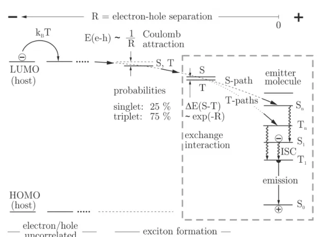
Figure 1.3: Simplified scheme of the exciton formation and recombination process in a host/guest system. E(e−h): binding energy of electron and hole,R: spatial separation of electron and hole, ∆E(S1−T1): energy separation of singlet (S) and triplet state (T), ISC: intersystem crossing. Adapted from references 23, 72.
emission quantum yield can be achieved in electroluminescent devices compared to purely fluorescent materials.5,8,13,23,40 In order to understand this different behavior, the mechanisms that lead to exciton formation in the emissive layer and as a result to the population of the excited states of the emitter molecules have to be analyzed. The following discussion of this is based on the one given in references 5, 23, 71, 72.
A simplified scheme of the exciton formation process is displayed in Figure 1.3. For the following considerations it is assumed that the EML consists of a host material in which the emitter is doped at a low concentration. Furthermore, it is assumed that an electron and a hole have already been injected into the EML and that the hole is already localized at the emitter molecule.
Driven by the external electrical potential the electron now starts to migrate towards
22 1 Introduction to Organic Light Emitting Diodes the hole through thermally activated hopping processes. Both particles can be considered as uncorrelated as long as they are far apart from each other. As the electron approaches the hole, Coulomb interaction between the oppositely charged particles becomes effective.
As a consequence of this electrostatic attraction, the distance between electron and hole decreases further. When the separationR between electron and hole falls below a critical valueRc both particles can be considered to form a bound state – an exciton. This is the case when the Coulomb energy E(e−h) becomes larger than the thermal energy Eth.
E(e−h) = e2 4π0R
=! kBT =Eth (1.3)
In this equation, e represents the elementary charge, 0 and the permittivity of the vacuum and the matrix material, respectively, kB the Boltzmann constant, and T the temperature.
According to this equation, if a value of = 3 is assumed, at ambient temperature an exciton is already formed at at a relatively large distance of electron and hole of about Rc = 180A. This means that electron and hole do not have to be located on one molecule in order to form a bound state but that they can still be separated by a large number of matrix molecules.
As soon as electron and hole are considered to be correlated also the spin of both particles has to be taken into account. As both particles carry a spin of1/2 the total spin of the formed exciton can either amount to S = 0, corresponding to a singlet state with multiplicity M = 1, or toS = 1, corresponding to a triplet state with multiplicityM = 3.
Consequently, electron and hole can form four different exciton states, one of them being a singlet and three of them representing the triplet. As at this point all states are nearly degenerate an even population of all four states is expected. In a statistical limit this leads to a ratio of singlet to triplet excitons of 1 : 3.73
When the electron approaches the hole within a radius of about 15A the wave functions of both particles may be regarded to start to overlap. At this point, the exchange interaction between the two particles cannot be neglected anymore. As a result, the formerly degenerate singlet and triplet states are now energetically split by twice the exchange integral.
Eventually, the attraction of electron and hole will lead to a localization of both particles on the same emitter molecule. This situation corresponds to this molecule being
1.3 Triplet Harvesting and Singlet Harvesting 23 in an excited state. Subsequently, the emitter molecule relaxes to the lowest excited singlet or triplet state depending on the total spin of the respective exciton. Typically, this occurs on a picosecond time scale or faster.
It is emphasized that from exciton formation to the population of the excited emitter states the spin is conserved meaning that singlet excitons can only populate singlet and triplet excitons only triplet states of the emitter molecule. As a consequence, 75 % of the emitter molecules will be in their lowest excited triplet while only 25 % will be in their lowest excited singlet state.
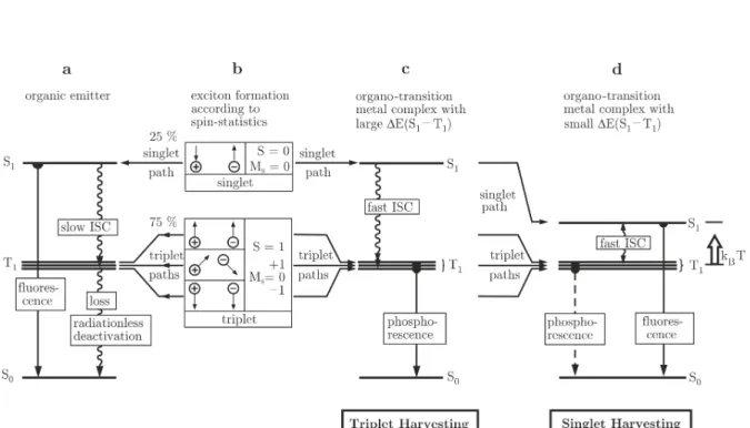
Starting from this situation (Figure 1.4b), the further relaxation processes depend on the class of the emitter material used. A graphical representation of possible relaxation paths is displayed in Figure 1.4 for three different emitter types.
In conventional purely organic molecules (Figure 1.4a) the population of the first excited singlet state S1 can result in an efficient radiative deactivation to the ground state via a fluorescence which typically occurs at a time scale in the order of several ns and with quantum yields of up to 100 %.63 Also an intersystem crossing process (ISC) from the S1 to the T1 state can occur. However, due to the absence of effective spin-orbit coupling (SOC) in purely organic molecules the time scale for this process is significantly longer (up to several milliseconds) than the fluorescence decay time.63 Therefore, the contribution of ISC to the deactivation of the S1 state can be neglected. In contrast to the highly allowed S1 →S0 transition, the T1 →S0 transition is strongly spin-forbidden.
This results in phosphorescence decay times which can be as long as several seconds.
As such long decay times favor the occurrence of nonradiative deactivation processes the probability for a radiative transition is rather small. Accordingly, in purely organic molecules only the singlet excitons (25 %) can be used for the generation of light in an electroluminescent device, while all triplet excitons (75 %) are lost for this purpose. This fact limits the internal quantum yield of OLEDs using fluorescent emitters to ηint = 0.25.
The situation is different when transition-metal compounds are looked at (Figure 1.4c).
In this case, the central metal atom induces significant SOC. As a consequence, the time constant for the ISC process is drastically decreased to values in the pico- or even femtosecond region.74–79 Under the condition that singlet and triplet state are separated by several 103cm−1, an emission from the singlet state cannot be observed anymore as almost all singlet excitations are transferred to the triplet state before a fluorescence can occur. Furthermore, SOC adds significant allowedness to the otherwise spin-forbidden transition from the triplet to the ground state. For compounds with particularly effective
24 1 Introduction to Organic Light Emitting Diodes SOC, emission decay times can be as short as 1 or 2µs, while emission quantum yields approaching 100 % can be achieved.5,26,27,56,64,65,80. Thus, in contrast to purely organic emitters, the triplet excitations are not lost for the emission process. As a consequence, OLEDs utilizing phosphorescent emitters can reach an internal emission quantum yield of ηint = 1. As according to this mechanism all excitations are collected in the triplet state, this is called the triplet harvesting effect.
On the other hand, in many other, especially 1st row, transition metal compounds SOC is significantly less effective which results in relatively long triplet decay times of up to several milliseconds.5,32,33,35,36,81 Emitters exhibiting such long decay times are rather ineffective when applied in OLEDs as pronounced saturation effects, such as triplet-triplet annihilation or efficiency roll-off, would occur.51 These problems can be overcome if the long triplet emission decay time does not become effective, for example, if emitters are used that exhibit only a small energy separation ∆E(S1−T1) between first excited singlet and triplet state, so that a thermal re-population of the singlet from the triplet state reservoir is possible at ambient temperature (Figure 1.4d). Such a mechanism corresponds to a thermally activated delayed fluorescence and leads to an effective reduction of the overall emission decay time as a significant part of all excitations is radiatively deactivated via the short lived singlet state.82 Moreover, in OLEDs utilizing TADF emitters all injected excitons, singlets and triplets, can be converted to light.
Consequently, the internal emission quantum yield of such devices can also amount to ηint = 1. In analogy to the triplet harvesting effect, this mechanism is termed singlet harvesting effect as at ambient temperature the radiative deactivation is occurring almost exclusively via the singlet state.5,13,33,35–37
1.3 Triplet Harvesting and Singlet Harvesting 25
Figure 1.4: Schematic representation of the electroluminescence excitation process for different emitter classes. (b) Spin statistics results in 25 % singlet and 75 % triplet state population. (a) In conventional purely fluorescent emitters, only emission from the singlet state occurs. All triplet excitations are lost for the emission of light. (c) In transition metal complexes all singlet excitations are transferred to the triplet state via fast intersystem crossing (ISC). From the triplet state, an efficient radiative deactivation through a T1 → S0 phosphorescence is possible. As a result, all excitations, singlets and triplets can be harvested in the triplet state and utilized for the generation of light (triplet harvesting effect). (d) In compounds that exhibit a small energy separation ∆E(S1−T1) between the first excited singlet and triplet state, a thermally activated delayed fluorescence (TADF) can occur. In this case, also all excitons can be converted to light but the emission results from the highly allowed S1 →S0 transition (singlet harvesting effect). Adapted from reference 5.
2
Photophysical Properties of Transition Metal Complexes
In the last chapter, it has already been pointed out that transition metal compounds possess high potential for application as emitters in electroluminescent devices. In this chapter, aspects of the electronic structure and emission properties of such complexes will be discussed. As this thesis focuses on the photophysical investigation of Cu(I) compounds, the following discussion will be centered around this material class. Where it seems necessary, also comparisons to the well investigated class of platinum and iridium compounds will be drawn.
2.1 Electronic States
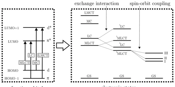
As for all transition metal complexes, also for Cu(I) compounds the emission properties are largely determined by their frontier orbitals, that are the highest occupied and lowest unoccupied molecular orbitals (MOs). From these MOs, the lowest excited electronic states result. In a rather simple approximation, the frontier orbitals can be described by the occupied π and unoccupied π∗ orbitals of the ligand(s) and the occupied d and unoccupied d∗ orbitals of the central metal ion. In such a model system, four different one electron excitations can occur. An illustration of this is given in Figure 2.1. It is noted that all considerations presented here are only valid for molecules exhibiting a singlet ground state.
The excitation of an electron from aπ to a π∗ orbital corresponds to a ligand centered (LC) transition. Hereby, π and π∗ orbitals are usually located on the same ligand.
28 2 Photophysical Properties of Transition Metal Complexes
Figure 2.1: Frontier orbitals and the resulting excited states of a transition metal com- plex. Only one electron excitations are displayed. Inclusion of the exchange interaction results in an energetic splitting of otherwise degenerate singlet and triplet states. If further spin-orbit coupling is included an energy splitting of the three triplet substates occurs. Adapted from reference 83.
However, in heteroleptic complexes, an electron can also be transferred from aπorbital of one ligand to theπ∗ orbital of another ligand. In this case, the process is termed ligand-to- ligand charge transfer (LLCT). In the literature, many examples for platinum compounds exhibiting ligand centered transitions have been reported. For copper compounds, this transition type is less relevant but also here some examples exist.78,84
Metal centered (MC) transitions occur if an electron is excited from a d orbital of the central metal atom to another unoccupied metal orbital. Typically, the unoccupied orbital is of d∗ type. In this case, the resulting dd∗ state can also be termed as ligand field (LF) state. In iridium and platinum compounds, these LF states generally are not the lowest lying excited states but they can be energetically close enough so that a thermal population from the emissive state can occur even at ambient temperature.
As LF states are frequently not emissive they represent a major source for nonradiative deactivation and even molecular dissociation, especially for blue emitting compounds in which emissive and LF state can be as close as only a few thousand wavenumbers. In contrast to this, LF states do not have an influence on the emission behavior of Cu(I)
2.1 Electronic States 29 compounds, as the d-shell of Cu(I) possesses a d10 configuration and is therefore fully occupied, so that no empty accessible d∗ orbitals and therefore no LF states exist. For this reason, Cu(I) compounds might be well suited for the development of stable blue emitters with high emission quantum yields. Moreover, in Cu(I) clusters, also metal centered ds∗ excitations can occur. In contrast to LF states these states can be highly emissive and contribute to the emission (compare for example reference 85).
Metal-to-ligand charge transfer (MLCT) transitions occur if on excitation significant charge is transferred from the central metal ion to one of the ligands. This transition type largely determines the emission behavior of most OLED relevant iridium and platinum complexes. In particular, through the involvement of the metal center in the emitting states, strong spin-orbit coupling can be induced which can result in high emission yields and short emission decay times. In contrast to this, for Cu(I) complexes SOC is significantly less effective (presumably) due to the smaller SOC constant of copper.
This would lead to distinctly longer emission decay times and smaller emission quantum yields. However, the charge transfer character is generally much more pronounced for copper compared to platinum and iridium complexes. As a consequence, a thermally activated delayed fluorescence can occur for Cu(I) compounds.
It is crucial to note that in this simple molecular orbital picture an important aspect, the interaction of the two unpaired electrons with each other, via Coulomb and exchange interaction, is neglected. An inclusion of these effects results in a splitting of each state, except for the ground state, into two states with different spin configuration, in the case of a singlet ground state into a singlet and a triplet excited state. These two states are energetically split by approximately twice the exchange integral K. The following example displays a situation frequently found in Cu(I) compounds. Typically, in such complexes the lowest excited singlet and triplet state is of MLCT character where the HOMO is mainly located on the d-orbitals of the metal center whereas the LUMO is mainly located on the ligand’s π∗ orbital. In this situation, the energy splitting between the first excited singlet and triplet state ∆E(S1−T1) is given by:
∆E(S1−T1)≈2K = 2
d(r1)π∗(r2)
e2 4π0r12
d(r2)π∗(r1)
(2.1) Hereby, d and π∗ represent the wavefunctions of the HOMO and LUMO, respectively, r1
and r2 the electron coordinates, and r12 their spatial separation. From this equation it is
30 2 Photophysical Properties of Transition Metal Complexes apparent that the exchange integral depends on the (spatial) overlap of the wavefunctions of the molecular orbitals involved in the transition. For a dπ∗ charge transfer transition, this overlap can be rather small as d and π∗ orbitals are located at different parts of the molecule. In this situation, a small exchange integral and therefore a small splitting between first excited singlet and triplet state result. The situation is different for localized transitions, for example for ligand centered transitions of ππ∗ character. In this case, a strong spatial overlap of the electron wavefunctions occurs as HOMO and LUMO are located at the same ligand. Consequently, the exchange integral and the splitting between first excited singlet and triplet state are large. More general, it can be stated that the singlet-triplet energy splitting decreases with increasing charge transfer character of the transition. It is remarked that the considerations made above only represent an approximation to the real situation found in transition metal complexes, where molecular orbitals typically consist of mixtures between ligand and metal centered orbitals. Accordingly, also the states represent mixtures.
2.2 Spin-Orbit Coupling
The central metal ion has a further strong impact on the properties of the electronic states of transition metal complexes. In particular, the metal center induces significant spin- orbit coupling (SOC) which results in fast intersystem crossing (ISC) between singlet and triplet states. For Pt(II) compounds, ISC times as fast as 50 fs have been observed.23,76 In contrast to this, for Cu(I) compounds significantly longer ISC time constants of about 10 ps have been reported.79,86,87 However, this is still orders of magnitude faster than time constants for prompt fluorescence which typically range between 1 ns and 100 ns.
As a consequence, prompt fluorescence can in general not be observed in transition metal complexes.
Furthermore, SOC allows an efficient coupling of different states. Of particular interest in this regard is the coupling of singlet states to the lowest excited triplet state.
Through this, significant singlet character can be mixed into this triplet state which adds allowedness to the otherwise spin-forbidden T1 → S0 transition. Consequently, short phosphorescence decay times and high emission quantum yields for this transition result.
Efficient coupling between two electronic states according to the direct SOC process can hereby only occur if the following three conditions are fulfilled:
2.2 Spin-Orbit Coupling 31 1. The interacting states must not result from the same molecular orbitals.
2. The two interacting states must result from two molecular orbitals that share the same metal center. Ideally, this metal center should exhibit a large SOC constant.
3. The interacting states must result from different metal d-orbitals.
From this it can be concluded that direct SOC is mainly effective for states resulting from molecular orbitals that have significant contributions from metal d-orbitals. Therefore, coupling between MLCT states is most efficient whereas LC states can neither couple to a MLCT nor to another LC state. For an evaluation of the SOC efficiency in real molecular systems the radiative T1 →S0 transition rate kr can be used. Hereby, it is important to note, that the three triplet substates, in the following marked with the index i, experience different admixtures from higher lying singlet states and therefore exhibit different radiative rates. A quantitative expression for kr(i) can be given by the following equation which is obtained from perturbation theoretical considerations:88
kr(i) = 64π4ν¯3 3hc3
X
m
hSm|HSO|T1(i)i E(Sm)−E(T1)
2
|hS0|er|Smi|2 (2.2)
In this equation, ¯ν represents the transition energy in wavenumbers,HSO the Hamilton operator for SOC, S and T the unperturbed wavefunctions of the coupling singlet and triplet states with the energies E(S) and E(T), respectively, ander the dipole operator.
Furthermore, SOC also leads to an alteration of the energies of the coupling states. For the three substates of the lowest excited triplet state T1, an energy stabilization occurs.
As each substate experiences different amounts of admixtures from higher lying singlet and triplet states, a different energy stabilization for each individual triplet substate results. Similarly as described above, also an expression for the energy splitting of the three triplet substates can be obtained from the perturbation theory formalism:88
E(i) = E(T1)−X
n,j
|hTn(j)|HSO|T1(i)i|2
E(Tn)−E(T1) −X
m
|hSm|HSO|T1(i)i|2
E(Sm)−E(T1) (2.3) This splitting is also observed in the absence of a magnetic field. Therefore, the energy separation of the energetically lowest and highest lying triplet substate is termed zero
32 2 Photophysical Properties of Transition Metal Complexes field splitting (ZFS).
For completeness it is mentioned that also the process of indirect SOC exists. However, this process is significantly less effective compared to the direct one. A more detailed discussion of this and other aspects of SOC can be found in reference 88.
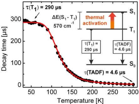
2.3 Temperature Dependence of Emission
In transition metal complexes emission is not occurring from a single electronic state.
For example, if other states are energetically close, they can be thermally populated and contribute to the emission. Hereby, each state exhibits an individual deactivation rate ki to the ground state. Under the assumption, that all states are in a fast thermal equilibrium, the states are populated according to a Boltzmann distribution and the total deactivation ratek(T) of all states to the ground state in dependence of the temperature T is given by:1,28,89
k(T) =
p
P
i=1
ki exph
−∆E(i−ik 0)
BT
i
p
P
i=1
exph
−∆E(i−ik 0)
BT
i (2.4)
In this equation, kB represents the Boltzmann constant and ∆E(i−i0) the energy separation between i-th state and the energetically lowest excited state i0. However, emission decay times τ are experimentally better accessible than rates k. Therefore, it is helpful to rephrase equation 2.4 accordingly, using τ =k−1. For a four level system consisting of the lowest excited singlet (S1) and triplet (T1) state, whereby the triplet consists of the three substates I, II, and III, the emission decay time can be written as a function of temperature according to the following equation:39,65,89
τ(T) =
1 +exph
−∆E(II−I)k
BT
i
+exph
−∆E(III−I)k
BT
i
+exph
−∆E(Sk 1−I)
BT
i
τI−1+τII−1exph
−∆E(II−I)k
BT
i
+τIII−1exph
−∆E(III−I)k
BT
i +τS−1
1 exph
−∆E(Sk 1−I)
BT
i (2.5) For molecular systems, in which no TADF occurs and in which therefore the en-
2.3 Temperature Dependence of Emission 33 ergetic separation between first excited singlet and triplet state ∆E(S1−I) is large (>3000 cm−1), the last term in the nominator and denominator in equation (2.5) is small
and can be neglected. This leads to:1,65
τ(T) =
1 +exph
−∆E(II−I)k
BT
i
+exph
−∆E(III−I)k
BT
i
τI−1+τII−1exph
−∆E(II−I)k
BT
i
+τIII−1exph
−∆E(III−I)k
BT
i (2.6)
A situation frequently found for Cu(I) complexes is that the zero field splitting (ZFS = ∆E(III−I)) is small (< 1 to 2 cm−1). In this case, it is justified to assume
∆E(II−I) = ∆E(III−I) = 0. Then, equation (2.5) simplifies to:
τ(T) =
3 +exph
−∆E(Sk 1−I)
BT
i
3τT−11 +τS−11 exp h
−∆E(Sk 1−I)
BT
i (2.7)
Note that ∆E(S1−I) often is also termed as ∆E(S1−T1).
Importantly, by fitting equations (2.5) – (2.7) to experimental data, more specifically to the temperature dependent behavior of the emission decay time, the energy splitting of the emitting states as well as their individual decay constants can be determined for the investigated compounds. As in contrast to Pt(II) and Ir(III)generally for Cu(I) complexes no highly resolved spectra can be obtained even at a temperature of T = 1.3 K (compare chapters 3 and 4) this indirect method provides detailed access to properties of
the electronic states.
3
Dinuclear Copper Complexes
In the last decades, Cu(I) complexes have been intensely studied due to their interesting luminescence properties. Research in this field has been additionally stimulated, since the potential of these compounds as emitters in organic light-emitting diodes was recognized.
Hereby, most investigations focused on Cu(I) complexes exhibiting one copper center that is pseudo-tetrahedrally coordinated by two bidentate ligands.5,6,28,33,35,38,42,78,79,84,86,87,90–99
In contrast to this, dinuclear Cu(I) compounds are significantly less explored, especially with regard to their emission behavior. Only recently, respective investigations have been published, suggesting that also this material class can show very promising properties at ambient temperature, such as short emission decay times, high emission quantum yields, and the possibility to tune the emission energy over a wide spectral range, from the deep blue to the dark red.13,30,32,37,100–106 In addition, for some of these complexes it was demonstrated that they exhibit a thermally activated delayed fluorescence,30,32,102,106
making them highly attractive for the use in OLEDs. Interestingly, the activation energy for the TADF process can be as low as only 350 cm−1 for the dimers,30,102 significantly smaller than for monomeric Cu(I) complexes for which the activations energies are typically about two to three times larger.5,6,28,33,35,39,42
Therefore, in this chapter a new class of Cu(I) dimers is studied in detail to get a deeper insight into the emission processes. The complexes represent dinuclear compounds in which one bidentate ligand is coordinated to each copper center and where the copper centers themselves are bridged by two halides. In the first section of this chapter, the investigation focuses on the influence of the halides on the emission behavior. In the second section, the ligands and the metal ions are modified to study the respective effects on the emission properties.
36 3 Dinuclear Copper Complexes
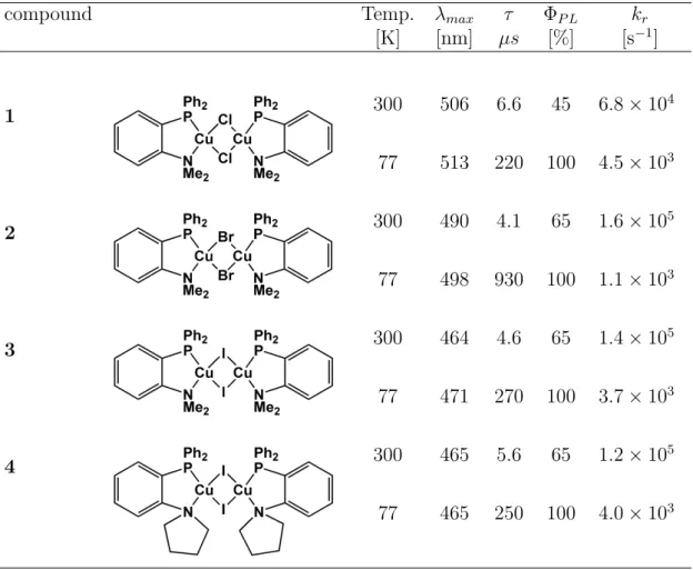
3.1 Complexes with Aminophosphine Ligands
In this section, the four halide bridged copper complexes [Cu(µ-Cl)(PNMe2)]2 (1), [Cu(µ- Br)(PNMe2)]2 (2), [Cu(µ-I)(PNMe2)]2 (3), and [Cu(µ-I)(PNpy)]2 (4) are investigated (compare Figure 3.1). The two copper centers in each compound are bridged by two halide atoms (chlorine, bromine, iodine). As chelating ligands, the aminophosphines Ph2P- (o-C6H4)-N(CH3)2 (PNMe2) and Ph2P-(o-C6H4)-NC4H8 (PNpy) are used. A detailed photophysical characterization is carried out focusing on the TADF mechanism and on the lowest excited singlet and triplet state properties. In particular, the triplet state, studied down to T = 1.3 K, reflects details of the effectiveness of spin-orbit coupling (SOC) in halide-bridged copper compounds. The discussion given in this section is
essentially following the one given in reference 36.
Figure 3.1: Chemical structures of compounds 1–4. Ph = Phenyl, Me = Methyl.
3.1.1 Crystal Structures
In Figure 3.2, the structures of the four investigated compounds are displayed as received from X-ray measurements.i Important interatomic distances and angles are summarized in Table 3.1.
Two different coordination structures were found for the investigated substances. In compound1, the copper and halide atoms are located in one plane representing a planar
iX-ray measurements were performed by Fritz-Robert K¨uchle, University of T¨ubingen
3.1 Complexes with Aminophosphine Ligands 37
Table3.1:Selectedinteratomicdistancesandanglesofthecoppercomplexes1–4asobtainedfromX-rayanalysesand fromDFTcalculationsperformedontheB3LYP/def2-SVPleveloftheory(calc.).X-raydatawereprovided byFritz-RobertK¨uchle,UniversityofT¨ubingen. compound1233(calc.)4 Cu(2)–X(1)[A]2.283(1)2.499(1)2.634(1)2.6952.646(1) Cu(1)–X(1)[A]2.369(1)2.418(1)2.582(1)2.6602.597(1) Cu(1)–X(2)[A]2.283(1)2.542(1)2.666(1)2.6952.646(1) Cu(2)–X(2)[A]2.369(1)2.417(1)2.590(1)2.6592.597(1) Cu(1)–Cu(2)[A]2.983(1)2.559(1)2.574(1)2.6892.688(1) Cu(1)–N(1)[A]2.305(2)2.248(1)2.250(3)2.5662.328(3) Cu(2)–N(2)[A]2.305(2)2.231(1)2.232(3)2.5732.328(3) Cu(1)–P(1)[A]2.175(1)2.190(1)2.210(1)2.2842.222(1) Cu(2)–P(2)[A]2.175(1)2.189(1)2.213(1)2.2832.222(1) Cu(1)–X(1)–Cu(2)[°]79.8(1)62.7(2)59.1(1)60.361.7(2) Cu(1)–X(2)–Cu(2)[°]79.8(1)62.1(2)58.6(1)60.361.7(2) X(1)–Cu(1)–X(2)[°]100.2(1)100.0(1)105.5(2)112.5107.4(1) X(1)–Cu(2)–X(2)[°]100.2(1)101.3(1)106.2(2)112.5107.4(1) N(1)–Cu(1)–P(1)[°]84.4(1)83.6(1)83.3(1)77.382.4(1) N(2)–Cu(2)–P(2)[°]84.4(1)85.0(1)84.2(1)77.182.4(1) X(1)–Cu(2)–Cu(1)–X(2)[°]0128.2(1)132.7(1)148.1139.6(1)
38 3 Dinuclear Copper Complexes
Figure 3.2: ORTEP representation (50 % ellipsoids) of compounds 1–4 from X-ray struc- ture determinations. Hydrogen atoms are not displayed for clarity. Crystal structures were provided by Fritz-Robert K¨uchle, University of T¨ubingen.
geometry of the copper halide core. In contrast, for the compounds 2–4 these atoms include distinct dihedral angles Br(1)–Cu(2)–Cu(1)–Br(2) of 128.2° (2), I(1)–Cu(2)–
Cu(1)–I(2) of 132.7°(3), and I(1)–Cu(2)–Cu(1)–I(2) of 139.6°(4) representing a butterfly type geometry of the copper halide core. Additionally, the orientation of the two ligands relative to each other differs between these two types of structures. More specifically, in the planar coordination, the phosphorus and nitrogen atoms of the ligands are in trans positions, whereas in the butterfly coordination they are in cis positions.
3.1 Complexes with Aminophosphine Ligands 39 An analysis of the interatomic distances of the substances containing the PNMe2 ligand (compounds 1–3) reveals that the lengths of the copper halide bonds (Cu(1)–X(1)) increases from 1 (2.369A) to2 (2.418A) to 3 (2.582A). This trend is also reflected in the other Cu–X bonds (Cu(1)–X(2), Cu(2)–X(1), and Cu(2)–X(2)) and is expected, as the radii of the halide atoms increase in the order Cl < Br < I. Moreover, a slightly larger Cu(1)–Cu(2) distance is found for 3(2.574A) than that for2(2.559A). Replacing the PNMe2 ligand (compound 3) by PNpy (compound 4) leads to a significant increase of the Cu(1)–Cu(2) distance to 2.688A due to the increased steric demand of the ligand, more specifically of the cyclopentyl groups. However, compound 1 exhibits the largest Cu(1)–Cu(2) distance (2.983A)), which is a result of the planar structure of the copper halide core of this molecule. Thus, large variations of the the Cu(1)–Cu(2) distances ranging from 2.56A to 2.98A are observed for the studied complexes1–4. Similarly large variations also occur for other halide-bridged dinuclear copper complexes.13,30,32,37,100–105
3.1.2 Computational Investigations
The type of the electronic transition and the characters of the involved molecular orbitals that contribute to the emission can be elucidated by carrying out density functional theory (DFT) and time-dependent density functional theory (TDDFT) calculations.
Applying the B3LYP functional and the def2-SVP basis set, as suggested by Jesser et al.,107 HOMO and LUMO contour curves are obtained for compound3for the (optimized) ground state geometry (Figure 3.3).
Figure 3.3: HOMO and LUMO of compound 3 for the ground state S0 geometry in the gas phase. The basis set used was def2-SVP. B3LYP was used as the functional.
40 3 Dinuclear Copper Complexes
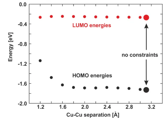
Figure 3.4: HOMO and LUMO energies of compound 1 in dependence of the Cu(1)–
Cu(2) separation. For the results marked with the small dots, the Cu(1)–
Cu(2) separations were constrained. The large dots indicate the results of a calculation without constraints. Calculations were performed on the B3LYP/def2-SVP level of theory.
The pronounced spatial separation of these frontier orbitals indicates that the HOMO–
LUMO transition possesses significant charge transfer (CT) character. More specifically, with an excitation charge is transferred from the d orbitals of the copper and the p orbitals of the iodine atoms to the unoccupied orbitals. The latter ones are mainly located on the PNMe2 ligands. Therefore, this transition can be assigned to be of (metal+halide)-to-ligand charge transfer ((M+X)LCT) character.
TDDFT calculations give an insight into the molecular orbital contributions to the electronic energy states. For example, for compound 3 the HOMO–LUMO transition contributes to the lowest excited singlet and triplet state by ≈ 90 % and ≈ 60 %, respectively. A further significant amount comes from the HOMO–2 to LUMO+1 transition, which amounts to ≈10 % for the singlet and ≈20 % for the triplet state. All contributing occupied orbitals (HOMO, HOMO–2) are located on copper and iodine, whereas all contributing unoccupied orbitals (LUMO, LUMO+1) are located on the
3.1 Complexes with Aminophosphine Ligands 41 ligands. This means that the lowest excited states represent 1,3(M+X)LCT states. Such a significant CT character is usually connected with relatively broad and unstructured spectra. Indeed, the experimentally determined emission spectra are broad even at low temperatures and thus in agreement with this prediction (see next section and Figure 3.5).
DFT calculations also allow to investigate the influence of the Cu(1)–Cu(2) separation on the emission behavior. For this, the geometry of compound 1 was optimized while the separation of the Cu(1)–Cu(2) atoms was constraint to values between 1.2A and 3.0A. Without the constraint, a Cu(1)–Cu(2) separation of 3.1A is found. Interestingly, in a wide range of Cu(1)–Cu(2) separations, from about 1.8A to 3.1A, the HOMO and LUMO energies do not change significantly, indicating that also the emission energy should not change. While the LUMO energy is not affected if the distance of the copper centers is further decreased to values below 1.8A, an increase of the HOMO energy is observed presumably due to metal-metal interactions and a red shifted emission would be expected. However, compounds that exhibit such small Cu–Cu separations are not known. Therefore, it can be concluded that the Cu(1)–Cu(2) separation has negligible impact on the emission energy, especially for the compounds investigated in this section.
A graphical representation of these results is displayed in Figure 3.4.
3.1.3 Spectroscopic Introduction
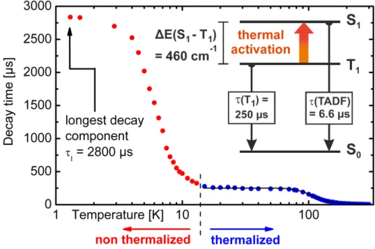
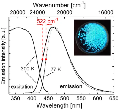
The studied compounds show intense blue (3, 4) and green (1, 2) luminescence under UV excitation. At first, the discussion will focus on the photophysical properties of compound 3. The measurements were performed with powder samples due to the limited chemical stability of the substances in solution.108 A justification for this approach is given below. Figure 3.5 shows the emission and excitation spectra measured at ambient and at liquid nitrogen temperature, respectively. With temperature variation, distinct changes of the emission properties are observed. At T = 77 K, the emission maximum lies at λmax(77 K) = 471 nm (50 % high energy flank at 443 nm), the decay time amounts to τ(77 K) = 270µs, and the quantum yield ΦP L(77 K) is as high as almost 100 %. According to this relatively long decay time and due to the detailed investigations at lower temperatures (T = 1.3 K, compare section 3.1.5), the emitting state at low temperature is assigned to be the triplet state T1 with a singlet ground state S0. With temperature increase to T = 300 K, a slight blue-shift of the emission to
![Figure 3.6: Emission spectra of substances [Cu(µ-Cl)(PNMe 2 )] 2 (1), [Cu(µ-Br)(PNMe 2 )] 2 (2), [Cu(µ-I)(PNMe 2 )] 2 (3), and [Cu(µ-I)(PNpy)] 2 (4) measured as powders](https://thumb-eu.123doks.com/thumbv2/1library_info/4647672.1608134/44.892.278.682.158.530/figure-emission-spectra-substances-pnme-pnme-measured-powders.webp)
![Table 3.3: Overview of the properties of the first excited singlet and triplet states of the investigated substances compound (powder) 1 2 3 4 ∆E(S 1 − T 1 ) a [cm −1 ] 460 510 570 630 τ (T 1 ) a [ µ s] 250 1200 290 250 τ (S 1 ) a [ns] 210 110 90 100 τ (TA](https://thumb-eu.123doks.com/thumbv2/1library_info/4647672.1608134/49.892.168.652.242.394/overview-properties-excited-singlet-triplet-investigated-substances-compound.webp)