Tailored nanoantennas for directional Raman studies of individual carbon nanotubes
Nicola Paradiso,*Fatemeh Yaghobian, Christoph Lange, Tobias Korn, Christian Sch¨uller, Rupert Huber, and Christoph Strunk Institute for Experimental and Applied Physics, University of Regensburg, 93040 Regensburg, Germany
(Received 17 January 2014; revised manuscript received 4 May 2015; published 29 June 2015) We exploit the near field enhancement of nanoantennas to investigate the Raman spectra of otherwise not optically detectable carbon nanotubes (CNTs). We demonstrate that a top-down fabrication approach is particularly promising when applied to CNTs, owing to the sharp dependence of the scattered intensity on the angle between incident light polarization and CNT axis. In contrast to tip enhancement techniques, our method enables us to control the light polarization in the sample plane, locally amplifying and rotating the incident field and hence optimizing the Raman signal. Such promising features are confirmed by numerical simulations presented here. The relative ease of fabrication and alignment makes this technique suitable for the realization of integrated devices that combine scanning probe, optical, and transport characterization.
DOI:10.1103/PhysRevB.91.235449 PACS number(s): 78.67.Ch,42.79.Dj,52.40.Fd,78.30.−j I. INTRODUCTION
Similar to antennas for communication systems, the operating principle of nanooptical devices consists in the ability to convey, focus, control, and reemit electromagnetic signals [1,2]. Interestingly, it is often the near field of nanoantennas which is exploited in applications, as it can be used to greatly enhance the field amplitude and custom-tailor the electric field distribution locally. The size and shape of the antennas can be designed to excite a plasmon resonance [3] or to focus [4] the optical near field to selectedhot spots[5].
A promising and direct application of nanoplasmonics is the surface-enhanced Raman spectroscopy (SERS) [6–9], where metallic structures are used as antennas in order to enhance both the cross section and the field intensity [10,11] for Raman scattering. The most effective structures employed in early SERS studies were colloidal gold or silver particles [12–14], which provide dramatic enhancement factors in correspon- dence to randomly distributed hot spots. For many applications this approach appears insufficient: to fully unfold the potential of modern nano-optics technology, it is desirable to fabricate tailored devices that locally manipulate the optical field in correspondence to a specific target region of the sample.
Such a top-down approach to SERS is at present an emerg- ing field [15–18]. First investigations employ patterned an- tenna structures to enhance the Raman signal of graphene [16].
This particular choice is motivated by the fact that the Raman spectrum of graphene is well known, and it is relatively easy to transfer a single layer on top of selected patterned struc- tures. However, owing to their extremely anisotropic optical properties, carbon nanotubes (CNTs) appear in many respects to be more intriguing candidates for target structures [19–22].
Raman spectroscopy of individual CNTs is usually difficult, due to their small cross section. The measured signal is significant only when either the incident or the scattered light is in resonance with an interband transition [23]. Raman spectra are typically obtained from an ensemble of CNTs, from which one can occasionally detect the signal of an individual CNT which satisfies the resonance condition. For this reason CNTs highly benefit from the field amplification provided by tailored
*nicola.paradiso@physik.uni-regensburg.de
optical antennas [19] that enable Raman signal enhancement of agiven CNT at a specific position, e.g., next to selected electrodes. This opens new scenarios for experiments that combine optical and transport measurements. Local SERS can be used to determine diameter, chirality, and number of defects for the portion of CNT contacted on a transport device. This information is often crucial for the interpretation of transport experiments [24], since many important physical quantities (e.g., spin-orbit interaction, Aharonov-Bohm flux, curvature-induced gap) depend on the diameter or on the chirality [25,26].
Compared to tip-enhanced Raman spectroscopy (TERS) [27–30], the use of patterned nanoantennas introduces a new degree of freedom, i.e., the possibility to rotate the electric field vector on the subwavelength scale. A mesoscopic field rotator could be harnessed to locally excite a specific CNT position. CNTs only absorb (and scatter) light with polarization parallel to their axis. Thus, by shining light polarized orthogonally to the axis, only the CNT portion in correspondence to the antennas will absorb light, while the rest of the CNT will effectively screen the radiation.
In the present work we investigate SERS of CNTs by making use of patterned arrays of nanoantennas. They allow us to acquire spectra even from CNTs whose Raman signal is too weak to be detected on the bare tube. From the amplified Raman spectra we can infer the local structure, the disorder, and the metallicity of CNTs. By polarization- dependent Raman spectroscopy we demonstrate that antenna arrays effectively rotate the electric field vector of the incident light. The experimental data are quantitatively discussed in light of the results of numerical simulations.
II. EXPERIMENTAL DETAILS
Figure1(a)shows the geometry of our structures, consisting of arrays of metallic strips with a well-defined orientation with respect to the axis of a single-wall CNT. The physical motivation behind choosing such a geometry is pictorially illustrated in Fig.1(b). The incident light effectively polarizes the metal strips, whose thickness is of the order of the skin depth (≈20 nm for gold in the visible range). At optical frequencies, the strips can be seen as parallel plate capacitors that couple the far-field radiation into electromagnetic surface
+ + + + + + + + + + + + + + +
- - -
- -E
iE
ind(c) (b)
E
T+ + + + + + + + + + + + + + +
- - -
2 ms
^z
^(a)
Ti/Au antennasSi/SiO2 substrate CNT
FIG. 1. (Color online) (a) Sketch of a Ti/Au nanoantenna array patterned on the Si/SiO2 substrate. The coupling with surface plasmon polaritons and thus the field enhancement depend on the angleαbetween the CNT axisˆzand the directionˆsorthogonal to the strips. (b) In some samples we have patterned three arraysA0◦,A30◦, andA45◦, whose angleαis 0◦, 30◦, and 45◦, respectively. Owing to the large aspect ratio of such structures, the incident fieldEiand the induced fieldEindare in general not parallel, since the latter is preferentially oriented along ˆs. (c) AFM micrograph of our sampleC, acquired after all measurements [31].
modes. Such correlated oscillations of charge density and electromagnetic field are called surface plasmon polaritons (SPPs) [32,33]. The periodic arrangement of antenna strips yields a spatially coherent standing plasmon wave which leads to a concentration of the electric field in the nanoscopic gaps between the strips. The resulting field enhancement within the array gaps is particularly useful when applied to Raman spectroscopy, since the Raman signal dependence on the field amplitude is nonlinear. If both the incident and scattered signal are magnified by the same factor η, then the Raman signal intensity scales asη4.
The particular design of our antenna arrays allows us to control not only the field magnification, but also the polariza- tion direction. The strip length is in fact much larger than both the optical wavelength and the spot size. We can therefore to first approximation neglect end effects and consider the direction of the induced field as constant in the middle of the strips, and orthogonal to them, as shown in Fig. 1(b). Such local control of the light polarization is particularly interesting when applied to target structures which have an intrinsically anisotropic optical response, as in the case of CNTs. Owing to their large aspect ratio, CNTs can effectively screen only the field component orthogonal to the axis. This property of CNTs (calleddepolarization effect[34,35]) makes them the ideal target to test the directionality of our antennas.
Our samples are fabricated starting from a p-doped Si substrate with a 500-nm-thick SiO2 cap layer. In a first lithographic step, the SiO2 surface is patterned with an array of rhenium markers, which exhibit excellent stability at the high temperatures required for the CNT growth. In a second lithographic step, we pattern an array of 1-μm-wide clusters of metallic nanoparticles [31] aligned to the rhenium markers. Afterwards, we grow the CNTs by chemical vapor deposition (CVD) [31]. This growth process yields almost exclusively single-wall CNTs, which are relatively straight and have a low number of defects compared to other techniques.
For such reasons, the CVD growth became the standard method to synthesize CNTs for low-temperature transport measurements [26]. In our samples the average yield is about 1–2 long CNTs per catalyst dot, so that in one chip we typically
have more than 100 tubes. CNTs start growing from the catalyst clusters and can extend up to tens of micrometers.
Owing to van der Waals interactions, CNTs tend to stick to each other during growth and often form bundles of few CNTs in the vicinity of the catalyst dot, where their density is higher.
In order to align the antenna structures to CNTs, we perform initial AFM scans to locate and identify individual CNTs on the substrate. Although slower compared to scanning electron microscopy (SEM) imaging, the AFM characterization does not contaminate the sample and allows us to check the quality of the surface topography. In addition, AFM scans provide a coarse estimate of the CNT diameter and allow us to determine whether the CNTs are isolated or grouped in a bundle, since we are able to follow a given CNT from the catalyst particle to the end.
Once a suitable CNT is found, nanoantenna structures are fabricated on top of it. An AFM scan of the final sample is shown in Fig.1(c). The nanoantennas studied in the present work consist of gratings of about 90-nm-wide and 4μm-long metal strips. The periodicity of the strips is 120 nm, so that the gap between them is approximately 30 nm. Each array contains nine strips, which define a 1-μm-wide and 4-μm-long rectangular pattern. The strips are designed via electron beam lithography using the preliminary AFM scans as a reference to align each array to the CNT. The metal deposition is obtained by thermal evaporation of a Ti (4 nm)/Au (17 nm) bilayer.
In most of our samples the antenna strips are oriented perpendicularly to the structures [as in the A0◦ array in Fig.1(b)]. For some particularly long CNTs (samplesAand C) we fabricated three arrays with different orientations. By definingˆsas the unit vector perpendicular to the strips andˆz as the CNT axis unit vector, the angleαbetweenˆs andˆzis 0◦, 30◦, and 45◦ for the top (A0◦), middle (A30◦), and bottom (A45◦) array, respectively. The separation between the arrays has been designed to be larger than the laser spot size, in order to obtain distinct optical signals from different arrays or in between two of them.
Our optical setup is equipped with two laser sources with wavelengths λL=532 and 633 nm. The former is highly absorbed by gold structures; thus we only use theλL=633 nm
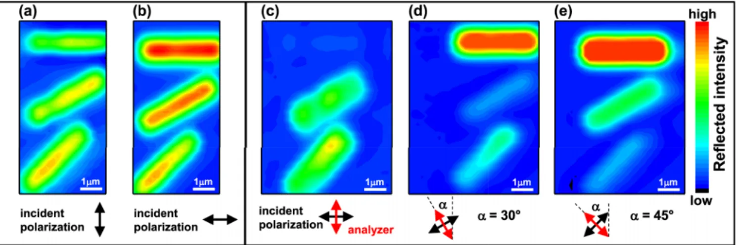
FIG. 2. (Color online) (a), (b) Reflectance measurements performed on sample C. The reflectance maps are obtained by scanning the sample while illuminating it withλL=633 nm light at normal incidence. The laser spot diameter is 1μm. The panels (a) and (b) correspond to the reflected signal acquired for incident light polarizationˆeioriented orthogonally and parallel to the topmost antenna array, respectively.
Both graphs show that the larger the angle betweenˆeiandˆs, the smaller the SPP coupling. This implies a reduced absorption and thus a larger reflected signal. (c)–(e) Crossed-polarization reflectance measurements on the same sample, withˆeiforming an angle of 0◦ (c), 30◦ (d), and 45◦(e) with respect to the vertical direction. In this case the presence of an analyzer oriented orthogonally toˆeiallows us to observe only the signal withrotatedpolarization. The reflectance maps demonstrate that the antennas effectively rotate the light polarization, except when this is nearly parallel to the strips.
wavelength for SERS measurements on antenna arrays. The excitation beam is focused onto the sample through a 100×
microscope objective, resulting in a spot size of about 1μm.
The polarization direction for the incident light is controlled via an achromaticλ/2 plate. Other details about our Raman setup have been reported elsewhere [36]. A given CNT with nanoantennas is easily found by means of Re markers. The determination of the CNT position is achieved by observing the antenna arrays with the objective and comparing the optical image with the preliminary AFM scans. With such a reference, we can place the laser spot exactly where the CNT crosses the patterned gratings, and acquire the corresponding local Raman or reflectance signal.
III. EXPERIMENTAL RESULTS
In order to prove the functionality of the nanoantennas, we have to demonstrate their ability to locally amplify the intensity and rotate the polarization of the incident light. The design of the antennas (and in particular the gap between the strips) has been chosen such that a SPP is excited when the array is illuminated with light at λL=633 nm. For the choice of the gap and strip width we refer to the work of Le Thi Ngoc et al. [37]. In this paper the authors present reflectance spectroscopy measurements on macroscopic arrays of gold strips. The experiment shows that an array of 80- nm-wide strips separated by a nominal gap of 20 nm is resonant atλL≈630 nm, i.e., at such wavelength the observed SPP coupling is maximum. The authors also show that the resonating wavelength increases when the gap is decreased, while the resonance width decreases for larger strip width.
We notice that for a nominal gap width of 20 nm, the actual one is roughly 30 nm [38], similar to the actual gap of our metal strips. Therefore, we expect to observe in our antennas a strong SPP coupling aroundλL=633 nm. Furthermore, such
coupling is expected to be anisotropic, owing to the elongated geometry of the metal strips.
The emergence of SPP and its angular dependence can be visualized by performing local reflectance measurements, where the sample is illuminated with light (λL =633 nm) polarized along different angles. The 1-μm-wide laser spot is scanned over the antennas and the reflected intensity is measured by a photodiode for each position. The results for sample C are shown in panels (a) and (b) of Fig. 2. For vertical polarization [Fig.2(a)], one expects to observe the best coupling for theA0◦array, since in this case the induced charge polarization is orthogonal to the strip. The larger the angle γ between ˆs and the incident polarization direction ˆei, the smaller is the expected coupling with the SPP. A larger coupling implies a more pronounced absorption and thus less reflected signal. This is precisely what we observe:
for incident light polarized vertically [Fig.2(a)] the reflected signal decreases from theA45◦ array (lowest coupling) to the A0◦array (optimal coupling). For horizontal polarization, the opposite is true [Fig.2(b)].
As previously mentioned, the excitation of a SPP in our nanoantennas implies a rotation of the polarization of the scattered field, which is then mainly oriented perpendicular to the strips. The polarization rotation can be directly imaged by crossed polarization reflectance measurements, where the reflected signal is filtered by an analyzer directed orthogonally to theˆeivector. The results of such measurements are shown in the panels (c), (d), and (e) of Fig.2for incident polarization directed orthogonally to the A0◦, A30◦, and A45◦ arrays, respectively. Clearly, the largest reflected signal is obtained for the antenna array directed at 45◦with respect to the incident field. The sharp angular dependence allows us to selectively suppress the signal coming from an individual array.
Reflectance measurements indicate that SPPs are excited in the nanoantenna arrays. As a consequence, the optical
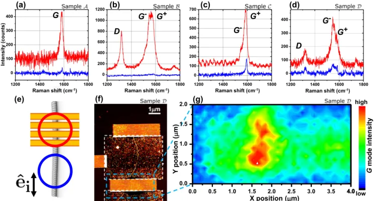
FIG. 3. (Color online) Raman spectra measured on samplesA(a),B(b),C(c), andD(d). The red curves correspond to the signal acquired on an antenna array orthogonal to the bundle, while the blue ones refer to the bare CNT portion immediately below the antennas, as sketched in panel (e). For all the curves we subtract a background signal acquired next to the CNT. For clarity, a shift of+100 counts has been applied to all the enhanced curves. The integration time is 30 s for all the spectra. Panel (f) shows an AFM scan of sampleD. To make the CNT visible, we increase the contrast of the areas indicated by the dashed-white rectangles. For sampleDwe scan the laser spot over the antenna area highlighted (dashed-blue rectangle) in the AFM scan in panel (f). Panel (g) shows the corresponding color map for the intensity of theG peak. A large signal is observed for the portion of CNT that crosses the antenna strips. The integration time is 5 s/pixel.
field is considerably amplified within the antenna gaps. This has a dramatic impact when applied to SERS, due to the nonlinear dependence of the scattered Raman signal on the field enhancement factor. In order to demonstrate the antenna- induced local enhancement, we perform a series of micro- Raman measurements on arrays fabricated on top of several individual CNTs or bundles. The results are summarized in Fig.3. The panels (a), (b), (c), and (d) show Raman spectra for theDandGmode, acquired on the samplesA,B,C, and D, respectively. From AFM scans we find that samples A, B, andCare most probably bundles of a few CNTs, whereas sample Dis an individual CNT [31]. The red curves in the reported spectra refer to the signal acquired on the portion of CNT or bundle underneath an array of orthogonal gold strips nominally identical to theA0◦structure in Fig.1(c). The blue curves show the corresponding Raman spectrum acquired on a bare CNT portion just above or below the array, as sketched in Fig. 3(e). A crucial finding of our measurements is that the signal measured on the optical antennas is systematically larger than the one measured on the bare CNT, despite in the former case only one quarter of the CNT length (i.e., the gap between two strips) is optically accessible. We define the signal amplification factorRas the ratio between the signal acquired on the antennas and the one measured on the bare CNT (or bundle). For samplesA,B,C, andDwe obtainR =8, 65, 3.5, and 5, respectively. The diversity ofRvalues will be discussed below in comparison to the results of field simulations.
The antenna-induced amplification allows us to extract useful information from samples whose spectrum would be otherwise barely discernible, as for the sample Aand B in Fig. 3. A low intensity of the Raman signal indicates that the process is not (or not perfectly) resonant, i.e., that the incident (or scattered) photon energy does not match any interband transitionEii of the CNT. For a given CNT and a given laser wavelength this is often the case. Optical antennas therefore allow one to increase the chances to observe the Raman spectrum from a specific CNT starting from a limited number of laser wavelengths. In our experiment we acquire spectra atλL=633 nm from about 12 structures (individual CNTs or bundles of few CNTs) and we observe a clear Raman signal (i.e., much larger than the background signal) for seven structures, a weak signal for one structure and nearly no signal for four structures. By comparison, without antennas we observe a clear signal only for one structure (sampleC), a weak signal for five structures, and no signal for all the other structures.
The measurement of theDand theGmodes provides direct information about number of defects (Dmode) and geometry (Gmode) of CNTs. In particular, theGmode is a fingerprint of the CNT chirality. Unlike graphene, the longitudinal optic (LO) and transverse optic (TO) component of theGmode are no longer degenerate in CNTs. One of the two components (the TO for semiconducting CNTs, the LO for the metallic ones) corresponds to atom displacements along the circumference
and is therefore softened by curvature effects [39–41]. There- fore, instead of the single peak observed in graphene, in CNTs theGmode is split in two components,G+ andG−, whose energy difference decreases with increasing the diameterd. In achiral (i.e., zig-zag and armchair) CNTs, however, only one of the two modes is allowed by symmetry [42], which makes them immediately identifiable in the spectra that show a singleGpeak. In metallic CNTs, the mode at lower energy G−is considerably broadened and softened by the interactions with the electron Fermi sea. Finally, the ratio between G+ andG− has been predicted to depend on the chiral angleθ, although there is no consensus yet about the precise functional form [43–45].
From the SERS spectra in Fig.3we can conclude that the bundle in sampleAcontains a semiconducting CNT which is relatively defect-free. SampleBcontains a metallic CNT with a higher concentration of defects. Sample C is of particular interest because the signal from the bare bundle is large enough to allow us to determine the impact of the antennas on the shapeof theG mode. It is evident that the enhanced signal is much broader and displays more structure compared to the single sharp peak measured on the bare portion [31]. In particular, the enhanced signal contains a metallic component (broadG− peak) which is absent in the bare bundle, whose spectrum corresponds to a semiconducting CNT with low chiral angle [40]. The occurrence of a structural change in the chirality of a CNT can be ruled out because the signal on the bare portion of sampleChas been acquired in between the arraysA0◦andA30◦. The shape of theGpeak measured on the antennas above and below the bare portion is identical [31].
We can therefore conclude that the antenna arrays enhance the Raman signal from different CNTs by different factors.
The interpretation of the enhanced spectra is more straight- forward for an individual CNT, as in sampleD. In this case, the observed CNT is clearly a chiral metallic one with a moderate number of defects. The enhancedGpeak has roughly the same shape of the peak measured on the bare CNT. On this sample, we also perform a Raman mapping of theGmode by scanning the laser spot over the area indicated by the dashed rectangle in Fig.3(f). The color map in Fig.3(g)shows the values of the integrated intensity of the G peak for each position of the laser spot. We notice that the signal is particularly intense only where the CNT intersects the antenna strips, whereas it is relatively low above and below the array.
The ultimate goal of Raman measurements on CNTs is the determination of the chiral indices (n,m) which fully determine the chiral angleθ and diameterd. More than a decade ago, Jorioet al.[23] described a method to assign the chiral indices based on the radial breathing mode (RBM) only. This method can only be applied to CNTs with an interband transition very close to the incident photon energy. Since the resonance window where the RBM is observable is particularly narrow (approximately 60 meV) [46], this condition is in general fulfilled only by a small fraction of a given set of CNTs.
Several authors [45–48] have shown that for individual CNTs the RBM alone is not sufficient to unambiguously determine the chiral indices. The information obtained from RBM must be combined with that deduced fromG mode features, i.e., the splitting and the relative intensity of the G+ and G−
peaks, and the width and shape of theG−. For instance, in our experiment the combination of RBM andG mode data (measured atλL=532 nm) allows us to conclude [31] that the bundleBlikely contains a (22,15) CNT. The bundleCcontains a semiconducting CNT with either (26,0) or (25,2) chiral indices (λL=532 nm) and a metallic CNT with either (21,6) or (20,8) chiral indices (λL=633 nm). For the last two cases, the pairs of possible assignments are adjacent members of the same familyp≡2n+m, wherepequals 52 and 48 for the semiconducting and the metallic CNT, respectively. Adjacent members of the same family share very similar properties and are therefore hard to distinguish by Raman spectroscopy [46].
Further details about our assignment procedure are discussed in the Appendixes.
We stress that for many applications the knowledge of the exact chiral indices is not strictly required. What is often needed is the metallicity, the density of defects, the approximate diameter and chiral angle, and eventually the presence of other CNTs. This information can be deduced from theDandGmode profiles, for which the possibility of a signal magnification is useful in case of experimental setups with only a few laser lines. On the other hand, the RBM signal acquired on the antennas is masked by a large background due to the light elastically scattered by the antenna surface. The tails of the large peak at zero Raman shift hinder the observation of low-frequency modes like the RBM. Thus all the RBM peaks measured in our experiment have been acquired on the bare portions of the CNTs.
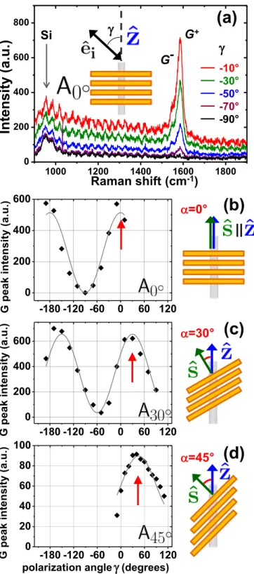
The anisotropic optical response of CNTs makes them ideal target samples to study the impact on SERS of the antenna orientation with respect to either the CNT axisˆzor the incident polarization directionˆei. Figure4shows how the Raman signal measured on sampleCdepends on the angleγ betweenˆeiand ˆz. Panel (a) displays selected Raman spectra measured on theA0◦ array for different γ angles. The graph in Fig. 4(b) shows how the measured amplitude of theGmode depends onγ. The maximum Raman signal (expressed in terms of the G-peak amplitude) is measured forγ ≈0◦ andγ ≈ −180◦, while it is clearly suppressed forγ ≈ −90◦. The experimental points can be fitted by a cos2γ function (gray curve in the graph). The cos2γ dependence is expected for two reasons.
On the one hand, the coupling between incident light and SPP is optimal for incident light polarized orthogonally to the array strips, while it is negligible for polarization parallel to the strips. On the other hand, owing to the depolarization effect, CNTs effectively screen the optical field directed orthogonally to their axis. As a consequence, the same angular dependence is observed also for the bare portion of the bundle [31].
The situation changes for theA30◦andA45◦ arrays, where the CNT axisˆzis no longer parallel to the array axisˆs. Thus, for negligible field enhancements, one would expect to observe the maximum Raman intensity forˆeiˆz. On the other hand, for sizable enhancements the incident fieldEi≡Eiˆeiis negligible compared to the SPP-induced field (Eind, which is parallel to ˆs) so that the total field is in this case parallel to the array axisˆs.
The data in Figs.4(c)and4(d)are better described by the latter scenario: the cos2γbehavior is reproduced, but the maximum intensity is observed at aroundγ =α, i.e., at γ =30◦ and γ =45◦for the arrayA30◦andA45◦, respectively.
FIG. 4. (Color online) (a) SERS spectra measured on the array A0◦ of sample C for different anglesγ between the CNT axis ˆz and incident polarization directionˆei. The small oscillations at lower Raman shifts are due to the signal elastically scattered by the antennas.
(b)Gpeak amplitudes plotted as a function ofγ (black dots). The same measurement has been repeated for the array A30◦ (c) and A45◦ (d). The gray curves in panels (b), (c), and (d) correspond to a cos2(γ−α) fit, withα=0◦, 30◦, and 45◦, respectively. All data have been suitably rescaled to take into account the dependence of the incident power on theλ/2 plate rotation [31]. Finally, the dark counts have been subtracted from all curves.
IV. DISCUSSION
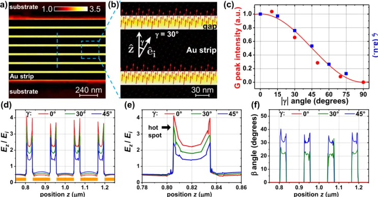
In order to better understand the SERS mechanism in the antenna arrays and to interpret the amplitude ratios of our spectra, we perform finite-difference frequency-domain (FDFD) simulations to calculate the total field in the vicinity of an array of gold strips for several orientations of laser polarization ˆei. The field enhancement is calculated for an incoming normalized plane wave polarized along the unit vectorˆeiforming an angleγwith theˆzdirection. The antenna strips are assumed to be orthogonal to the CNT (i.e., ˆs ˆz, as for theA0◦ array). The color scale of Fig.5(a)shows the modulus of the total electric fieldET ≡Eiˆei+Eind, for the particular case of ˆei directed at 30◦ with respect to ˆs. The direction and magnitude of the total field is shown in Fig.5(b) as arrows superimposed on the amplitude color map. We repeat the calculation for several values ofγ. For each of them we calculateEz≡(ET ·ˆz), i.e., the projection of the total electric field on the CNT axis. This is the only field component that can induce a Raman signal on CNTs, owing to the depolarization effect.
In Figs.5(d) and5(e)we plot the calculated Ez/Ei as a function of the CNT axis coordinatezforγ =0◦, 30◦, and 45◦. The graph clearly shows that the local field enhancement is large close to the edge of the metal strips, where the spikes occur. Here the local field enhancement is approximately 4.
For largest field enhancements we expect to have the most pronounced field rotation induced by the antennas. In other words, if |Eind|/Ei 1, then Eind≈ET and therefore the angleβ betweenET andˆeiwill tend toγ. Figure5(f)shows the profile ofβ(z) along the CNT axis. We notice that the higher the enhancement factor, the more the angleβ approachesγ.
This is consistent with the observations on macroscopic arrays of metal nanowires [37].
In order to compare the simulation results with the ex- perimental points in Fig.4(b)we compute the quantityζ ≡ (Ez(z)/Ei)2dz, i.e., the incident field intensity integrated over the four central metal strips of the array A0◦. The ζ value is proportional to the total Raman cross section and consequently it can be used to estimate the relative Raman intensities as a function ofγ. In fact, the scattered Raman signal is already directed along ˆz and does not affect the γ dependence. The graph in Fig. 5(c) shows a comparison between the measuredGpeak amplitudes (red dots) for the A0◦array of sampleCand the corresponding computedζ(blue squares), both plotted as a function ofγ. We also show a cos2γ fit for the experimental points. Although the fit is computed for the experimental data, the curve matches nicely the computed ζ(γ) points. This indicates that the impact of the angle γ consists in approximately rescaling the local enhancement by a factor cos(γ).
While theγ dependence of the relative Raman signal is correctly reproduced by our calculations, the interpretation of the absolute enhancement factors requires more care. In fact, the experimental values for the amplification factorR are quite diverse, ranging from 3.5 to 65. Such variability can be explained by the characteristics of each antenna array, e.g., contamination from the fabrication process, or surface roughness due to an imperfect lift-off of the antennas. We use the results of the field simulation to establish whether
FIG. 5. (Color online) (a) Finite-difference frequency-domain calculation for the specific case ofγ =30◦. The color plot shows the local value of|ET|/Ei, whereET is the total electric field. (b) Zoom-in on the region indicated by the cyan-dotted square in panel (a). The arrow pattern shows the local orientation of theET vectors (red arrows). (c)|γ|dependence (blue squares) of the Raman cross section for the array A0◦, calculated by integrating (Ez(z)/Ei)2over the cyan-dotted segment in panel (a). For comparison, we display (red dots) the experimental points [Fig.4(b)] together with a cos2γ fit (red curve)of the measured data. The graph has been normalized such that the value forγ =0◦ equals 1 for both experimental and simulated data. (d) SimulatedEz(z)/Eivalues plotted as a function of thezcoordinate along the segment highlighted in the panel (a). The red, green, and blue curves correspond to theγ=0◦,γ =30◦, andγ =45◦cases, respectively. (e) Zoom-in on a gap between two strips. The field is mostly concentrated within approximately 5 nm around the strip edge, in the so-calledhot spots.
(f) Calculated angleβbetweenET andˆeiplotted as a function ofzalong the same range and for the sameγvalues as in the panels (d), (e).
or not the observed variability of the enhancement factors can be ascribed to imperfections in the antennas. The field simulation allows us to estimate the ideal enhancement factor in the absence of imperfections. We assume that both the incident and the scattered light are amplified in the same way by the antennas. For theGmode the energy difference between incident and scattered light is ωG≈0.2 eV, comparable to the width of the SPP resonance [37]. Thus, if the optical antennas are effective for both frequencies, the resulting enhancement will be proportional to the fourth power of the local electric field [7,16]. In this approximation, the calculated amplification factor R expected from the model is about 14 [31]. In most of the measured samples we observe an amplification factor lower than 14, which could be due to imperfections. A few samples (e.g., sample B), however, display considerablylargerRvalues. Such unexpectedly large enhancements can be explained by the so-called chemical SERS [10]: besides enhancing the electromagnetic field, optical antennas can also directly exchange electrons with the CNTs. The resulting increase of the Raman cross section provides an additional amplification mechanism. This effect is much more pronounced in metallic CNTs, as demonstrated by SERS experiments with colloidal Ag or Au clusters [10,11].
Chemical SERS can explain the change in theGpeak shape observed for some bundles. If the signal from metallic CNTs is disproportionately amplified, one can observe the appearance
of a broadG− component not present in the spectrum of the bare CNT, as seen for instance in sampleC.
V. CONCLUSIONS
In conclusion, we have demonstrated SERS on individual CNTs and bundles using top-down patterned nano-antenna arrays. We obtained field amplification factors between 3.5 and 65, which allowed us to characterize CNTs whose Raman signal was not, or just barely, detectable without antennas. Owing to the particular geometry of our antennas, the induced field is rotated with respect to the polarization of the incident light, as verified by polarization-dependent SERS measurements.
The fabrication of patterned nanoantennas can be directly applied to transport devices to extract structural information in the vicinity of the CNT portion of interest. Furthermore, the ability to locally manipulate both modulus and direction of the optical field can be exploited to extract the local Raman signal of generic target molecules distributed on a substrate, e.g., by employing crossed-polarized configuration to suppress the signal everywhere but at the antenna position.
ACKNOWLEDGMENTS
We want to thank C. B¨auml for the help with the measure- ments, D. Steininger for the assistance with the growth of the
CNTs, and J. Maultzsch for helpful discussions. The work was funded by the European Union within the STREP “SE2ND”, and by the Deutsche Forschungsgemeinschaft within Grants No. SFB689, No. SFB631, and No. GRK1570.
APPENDIX A: CARBON NANOTUBE GROWTH Our fabrication process begins with electron beam lithog- raphy (EBL) of 20-nm-thick Re markers, which are used as a reference both for the alignment of the subsequent lithographic steps, and for the global positioning of the laser beam during the Raman measurements. In a second step we exploit again EBL to deposit clusters of catalyst nanoparticles on the sample surface. We spin two layers of poly-methyl- methacrilate (PMMA), whose thickness is 320 and 70 nm, respectively. We design the catalyst spots by EBL, using the Re markers as a reference. Then we dip the sample in a methanol solution of bis(acetylacetoneato)dioxomolybdenum(VI), alu- minum oxide, and ferric nitrate nonahydrate. We dry the solvent out and we remove the PMMA mask in acetone.
Then we insert the sample in a quartz tube positioned inside a furnace. The chemical vapor deposition (CVD) is performed in a steady flow of methane (10 sccm) and hydrogen (20 sccm) at 850◦C for 20 min. This recipe produces a number of CNTs per catalyst dot. In general, however, only a few of them are longer than 1μm. Each dot has on average 1 CNT longer than 10μm.
After the CNT growth we image the surface with an atomic force microscope (AFM) in tapping mode. These scans are used to check the presence of CNTs, their approximate diameter, and their exact position with respect to the Re markers. As a last step, we fabricate the nanoantennas. We exploit the previous scans to correctly align the strip arrays on the Re markers (and therefore on the CNT). The antennas are fabricated by depositing 4 nm of Ti and 17 nm of Au by thermal evaporation. Owing to the small gap between the antenna strips, the lift-off of the metal layer is particularly critical. We perform a second AFM scan in order to check the quality of these structures, and the actual CNT position within the gratings.
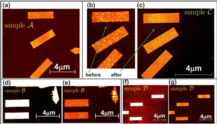
Figure 6 shows AFM topography scans of the samples studied in the present work. The panels (b) and (c) show the topography of sample C before and after the measurement session. We notice that contamination appears after the measurements which were not presentbefore[panel (a)]. This contamination is localized exactly in the areas where the laser spot was focused for most of the time. Its origin is a sort of optical tweezer effect, i.e., the attractive interaction that results from very intense optical fields on small particles in the vicinity. This effect is relevant only for sampleC, which has been subjected to the long reflectance measurements.
The Raman measurements, performed before the reflectance measurements, have not been affected by such contamination.
From AFM analysis we deduce that sampleAhas a diameter of (5.0±0.5) nm, sampleBhas a diameter of (2.5±0.5) nm,
4 m 4 m
4 m 4 m
4 m 4 m
before after
(a) (b) (c)
(d) (e) (f) (g)
FIG. 6. (Color online) Atomic force microscopy scans of the samples discussed in the present work. (a) AFM scan of sampleAperformed before the Raman measurements. (b) AFM scan of sampleCperformed before the Raman measurements. (c) The same sample scanned after all the measurement sessions. The topography reveals the presence of contamination exactly in the areas where the laser spot was focused.
(d) AFM scan on sampleB. The contrast has been exaggerated in order to show the CNT. (e) The same scan displayed with lower contrast.
(f) AFM scan on sampleD. The contrast has been exaggerated in order to show the CNT. (g) The same scan displayed with lower contrast.
(a) (b)
2 m 40nm
FIG. 7. (a) SEM micrograph of nanoantenna arrays nominally identical to the arrays in sampleC. (b) Zoom-in on the central array.
sampleChas a diameter of (4.5±0.5) nm, and sampleDhas a diameter of (1.5±0.3) nm.
Figure7shows two scanning electron microscope (SEM) micrographs of a replica of sampleC, i.e., a nominally identical device fabricated together with the original sample.
APPENDIX B: ESTIMATE OF THE CHIRAL INDICES The assignment of the precise chiral indices to individual CNTs on a substrate is not a trivial task, in particular when there are only few laser lines available. More than a decade ago, Jorioet al.[23] proposed a method to assign the chiral indices based on the RBM only. The method relies on the fact that the Raman signal from individual CNTs is too weak to be detected, unless the incident laser light is in resonance with an interband transition of the CNT (resonant Raman scattering). The authors therefore start from a large ensemble of CNTs distributed on a substrate and perform micro-Raman measurements on several positions. If a clear RBM signal is measured in a specific position, the corresponding diameter is extracted. Then a Kataura plot is used to find which CNTs have an interband transition close (within 100 meV) to the laser photon energy.
The information provided by the RBM measurements alone are certainly useful, but unfortunately its uncertainty is too large to allow one to safely determine the exact chiral indices. This has been pointed out several times in the literature [45–48]. For this reason, in recent years several experimental groups have developed alternative techniques (e.g., Rayleigh scattering or electron diffraction) that provide an independent determination of the chiral indices for free-standing CNTs.
Nowadays it is clear that the determination of the chiral indices of individual CNTs by Raman spectroscopy must take into account all the available information: RBM frequency, G peak shape, and laser frequency. This data may be combined with AFM topography to yield accurate results. In the following paragraphs we explain the procedure we have followed to extract the chiral indices from samplesBandC.
SampleB,λL =532nm. AFM analysis shows that sample Bis a bundle with diameter of roughly 2.5 nm. As explained in the main text, the light elastically scattered from the antenna surface is particularly disturbing for low Raman shift, therefore the RBM measurements have been performed on the bare portion of the CNTs next to the antenna structure.
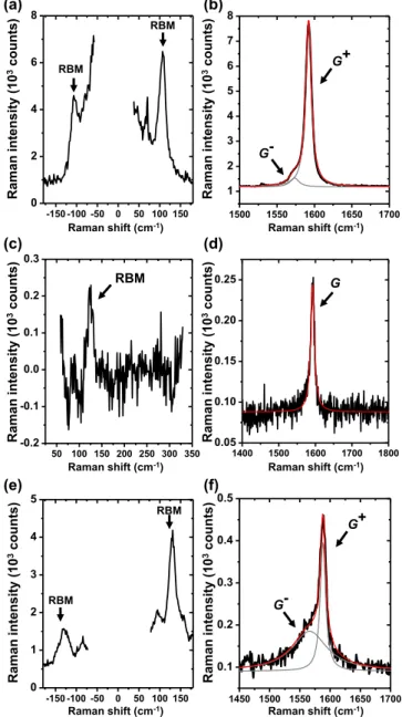
In the case of sampleB, we focus the laser spot on the bundle segment just below the array. The measurement with red light did not reveal any clear RBM peak, while using green light (λL=532 nm) we find a peak at (107±1) cm−1, as shown in
FIG. 8. (Color online) (a) Raman spectrum measured on sample Busing a laser source atλL=532 nm. The laser spot was placed on the bare portion of the bundle just below the antenna array. Both the Stokes and anti-Stokes peaks are visible. The RBM frequency is ωRBM =(107±1) cm−1. (b) Raman spectrum around the G mode frequency, together with a double-peak Lorentzian fit (red curve) showing the G− and G+ components (gray curves). (c) Raman spectrum measured on the bare portion of sampleC using a laser source atλL=633 nm. The RBM frequency isωRBM = (125±2) cm−1. (d) Raman spectrum around theGmode frequency, measured on the same position, together with a Lorentzian fit (red curve). (e) Raman spectrum measured on the bare portion of sampleC using a laser source atλL=532 nm. Both the Stokes and anti-Stokes peaks are visible. The RBM frequency isωRBM=(130±2) cm−1. (f) Raman spectrum around theGmode frequency, together with a double-peak Lorentzian fit (red curve) showing theG− and G+ components (gray curves).
TABLE I. Chiral indices for the CNTs within the window [d=(2.52±0.04) nm;Eii=(2.33±0.100) eV]. The values of the interband transitions have been taken from Ref. [49], with a 40 meV redshift correction to account for the substrate interaction.
(n,m) d θ [Eii;i] EL−Eii Metallicity (26,10) 2.521 nm 15.6◦ [2.28 eV;5] −0.050 eV Semicond.
(22,15) 2.525 nm 23.8◦ [2.34 eV;5] 0.009 eV Semicond.
(19,18) 2.510 nm 29.1◦ [2.39 eV;5] 0.059 eV Semicond.
Fig.8(a). The first problem is to convert this frequency into an estimate for the diameter. From the literature we know that the RBM frequencyωRBM depends linearly on the reciprocal of the diameter 1/d. However, the interaction with the substrate causes a slight deviation from the perfect proportionality. A more accurate functional dependence is the following [50]:
ωRBM =227 d
1+Cd2, (B1)
whereCis a substrate-dependent constant,ωRBMis expressed in cm−1, and the diameter in nm. The constantC for SiO2
reported by Saito et al. [50] is 0.065. Such constant is however based only on a single experimental point [23]. More recently, Pailletet al.[51] have made an extensive RBM study on many free-standing CNTs, using electron diffraction to independently determine the precise diameter. The empirical dependence found by Pailletet al.is
ωRBM = 204
d +27, (B2)
where again ωRBM is expressed in cm−1 and the diameter in nm. The two functions in Eqs. (B1) and (B2) are very similar in the diameter range of our interest (1–2 nm): their difference (≈40 pm) is of the order of the uncertainty due to the typical error in the determination of the RBM peak center (≈1−2 cm−1).
Since for sampleBwe measureωRBM =(107±1) cm−1, we deduce a diameterd=(2.52±0.04) nm. In this diameter range we search for all the CNTs that have an interband transitionEiiclose to the laser photon energyEL=2.33 eV (λL=532 nm). Following the literature [23,46], the window of acceptable values forEii is set toEL±100 meV, where 100 meV corresponds roughly to twice the width of the Raman resonance for the RBM. To this end, we use the experimental interband values reported in recent extensive Rayleigh spec- troscopy experiments [49]. The values have been corrected (i.e., ≈40 meV red-shifted) in order to take into account the effect of the substrate [52]. Among all the possible candidates, we choose only semiconducting CNTs, since the G peak profile measured with the same laser wavelength is compatible with a semiconducting CNT. In fact, the Lorentzian fit in Fig. 8(b) shows that the G− component occurs at a frequency well above 1550 cm−1. Table I lists the three CNTs which have diameter and an interband transition within the region of interest [i.e., d =(2.52±0.04) nm; Eii = (2.33±0.100) eV]. Two of them [(26,10) and (19,18)] are however quite off-resonance (|Eii−EL|>50 meV), which does not seem compatible with the fact that we observe a RBM signal also with relatively low integration time (<5 s).
TABLE II. Chiral indices for the CNTs within the window [d=(2.05±0.04) nm; Eii=(1.959±0.100) eV]. The values of the interband transitions have been taken from Ref. [49], with a 40 meV redshift correction to account for the substrate interaction.
(n,m) d θ [Eii;i] EL−Eii Metallicity (26,0) 2.036 nm 0◦ [1.98 eV;4] 0.21 eV Semicond.
(25,2) 2.041 nm 3.8◦ [1.98 eV;4] 0.021 eV Semicond.
(24,4) 2.055 nm 7.6◦ [1.98 eV;4] 0.021 eV Semicond.
(19,11) 2.059 nm 21.2◦ [2.05 eV;4] 0.091 eV Semicond.
(23,6) 2.077 nm 11.3◦ [2.00 eV;4] 0.041 eV Semicond.
(22,8) 2.108 nm 14.9◦ [1.98 eV;4] 0.021 eV Semicond.
(18,13) 2.112 nm 24.7◦ [2.04 eV;4] 0.081 eV Semicond.
Therefore, we assign to this CNT the chiral indices (22,15).
We stress that such chiral indices do not refer to the metallic CNT that produces the Raman spectrum displayed in Fig.2.
That spectrum was in fact acquired using theλL=633 nm laser source and therefore refers to another CNT in the same bundle. Finally, we notice that the diameter of the (22,15) CNT (d=2.52 nm) is compatible with the bundle diameter found by AFM (d ≈2.5 nm). This indicates that the (22,15) is the largest CNT of the bundle.
SampleC,λL=633 nm. The sample C displays a RBM peak for both laser wavelengths at our disposal, i.e.,λL=633 and 532 nm.
We start our analysis from the former case. The Raman spectrum around the RBM and theGmode is displayed in Fig.8(c). TheG peak shape displays only one component:
theG− component is either very low or absent. The Raman spectrum is well fitted by a single Lorentzian peak, as shown in Fig.8(d). This corresponds to either an achiral CNT, or to a CNT with low chiral angle. This considerably restricts the number of possible candidates. The RBM peak is centered at 125 cm−1. The peak is weaker than in the previous case; thus we consider here a larger uncertainty, i.e.,±2 cm−1. Using Eq. (B1), we deduce a diameterd =(2.05±0.04) nm. In the window [Eii =(1.959±0.100) eV; d =(2.05±0.04) nm]
we find seven possible CNT candidates, listed in Table II.
They are all semiconducting. Only two of them have a small chiral angle, compatible with the observation of a negligible G− component [40,43,44], namely (26,0) and (25,2). These are two adjacent elements of the same family 2n+m=52, which share very similar properties and are therefore difficult to discriminate. Therefore, we consider both (25,2) and (26,0) as possible chiral indices for the spectra of Figs.8(c)and8(d).
SampleC,λL=532 nm. Using the laser source atλL = 532 nm we obtain the Raman spectra in Figs.8(e)and8(f)for the RBM and theGmode, respectively.
We notice that theG mode is clearly metallic, owing to the presence of a broadG−component at around 1550 cm−1, as shown in Fig.8(f). The RBM peak is centered at (130± 2) cm−1, which corresponds to a diameterd =(1.95±0.04) nm. TableIIIshows the two metallic CNTs [(21,6) and (20,8)]
within the window [Eii =(2.330±0.100) eV; d =(1.95± 0.04) nm]. Between them, the most likely assignment is (21,6), owing to the smallerEii−ELvalue [53].
TABLE III. Chiral indices for the CNTs within the window [d=(1.95±0.04) nm;Eii=(2.33±0.100) eV]. The values of the interband transitions have been taken from Ref. [49], with a 40 meV redshift correction to account for the substrate interaction.
(n,m) d θ [Eii;i] EL−Eii Metallicity (21,6) 1.923 nm 12.2◦ [2.39 eV;2] 0.059 eV Metallic (20,8) 1.957 nm 16.1◦ [2.40 eV;2] 0.069 eV Metallic
APPENDIX C: RAMAN MEASUREMENTS ON THE BARE PORTION OF SAMPLEC
Figure9shows theγ dependence of the Raman spectrum around theGmode for the portion of bare bundle in between the antenna arraysA0◦andA30◦in sampleC. The measurement completes the data shown in Fig.4. Owing to the depolarization effect (discussed in the main text), the maximum signal is observed for |γ| =0◦, while for|γ| =90◦ it is completely suppressed. As expected theγ dependence is well fitted by a cos2γ function.
Figure10shows a comparison between a Raman spectrum measured on theA0◦ array of sampleC (blue curve), the one acquired on theA30◦array (red curve), the one acquired on the A45◦ array (green curve), and the one measured in the bundle portion betweenA0◦andA30◦(black curve). For better visibility we normalize the four curves to the sameGpeak amplitude.
We also subtract the background signal from all the curves, by measuring the signal next to the CNT. The graph shows that the spectra measured on the antennas are similar to each other, but they look quite different from the spectrum measured on the bare bundle. In particular, the spectra measured on the antennas show a broadG− component at around 1550 cm−1, a clear indication of a metallic CNT. On the contrary, the spectrum measured on the bare portion displays only one component.
Since this portion is located in between theA0◦andA30◦arrays, we cannot explain this change as a structural change occurring to the same CNT, since the spectra onA0◦ andA30◦ are the same. In the main text we explain such change in terms of a
FIG. 9. (Color online) (a) Raman spectra measured on the bare portion of sampleCbetween the antenna arrayA0◦ andA30◦. Each curve refers to a differentγangle. (b)Gpeak amplitudes plotted as a function ofγtogether with the best fit forAcos2(γ+φ)+I0, where A,φandI0are fitting parameters (best fit:A=164,φ=1.7◦, and I0=0.7).
FIG. 10. (Color online) Raman spectra around theGpeak mea- sured on sampleC. The blue, red, green, and black curves refer to the signal measured onA0◦,A30◦,A45◦, and on the bundle portion betweenA0◦andA30◦, respectively. The curves have been offset and rescaled in order to display the sameGpeak amplitude.
disproportional SERS enhancement of a metallic CNT within the bundle due to the so-calledchemicalSERS.
APPENDIX D: SERS ENHANCEMENT DEPENDENCE ON THE ANGLEα
In the main text we discuss the impact of the angle γ between the CNT axis ˆz and the incident polarization ˆei,
FIG. 11. (Color online) When the unit vectorsˆs(array axis), ˆz (CNT axis), andˆei(incident polarization direction) are noncollinear, the Raman process can be approximately described as the result of a series of field projections: the incident electric fieldE0ˆei is first amplified and projected toˆsby the antenna array. Then it is projected to ˆzowing to the depolarization effect. At this point, the scattered Raman intensity is then proportional to cos2γ cos2α. The Raman scattered light is again amplified and projected toˆs, thus providing a further cos2αfactor.
assuming constant the angleαbetweenˆzand the array axisˆs. In this section we discuss more in detail the general case, whenˆs, ˆz, andˆeiare noncollinear. The situation is sketched in Fig.11.
If the incident light excites a SPP, the field is amplified and rotated towardˆs. The coupling with the antennas (and thus the amplitude of the induced field) is proportional to cosδ, where δ≡α−γ. Hence the intensity of the total field illuminating the antennas is in good approximation proportional to cos2δ.
Owing to the depolarization effect, only the component of the resulting field along the CNT axis ˆz will produce a Raman signal, which will then be proportional to cos2α. The scattered Raman signal is emitted preferentially along the CNT axis. Thus, if also the scattered frequency excites a SPP in the antennas, then this will be again amplified and rotated alongˆs. Since only the component of the scattered field along
ˆs can excite a SPP, we expect an additional cos2α factor.
Therefore, under these assumptions, in the general case the measured Raman signal will be proportional to cos2δcos4α.
In particular for a givenα, we expect to observe a cos2(γ−α) dependence, in agreement with the data in Fig.4.
We stress that it is not easy to quantitatively verify the general α dependence, since this requires one to compare different antenna arrays that can be more or less affected by contamination or fabrication imperfections. Moreover, single-wall CNTs are usually not straight and this introduces an uncertainty in the determination of theα angle over the antenna array width. Nevertheless, in our sample we observe in most cases a decay of the Raman signal for largeαangle, even though the present uncertainties do not allow us to verify quantitatively the cos4αdependence.
[1] L. Novotny,Phys. Today64,47(2011).
[2] L. Novotny and N. van Hulst,Nat. Photon.5,83(2011).
[3] W. A. Murray and W. L. Barnes,Adv. Mater.19,3771(2007).
[4] M. Schnell, P. Alonso-Gonz´alez, L. Arzubiaga, F. Casanova, L. E. Hueso, A. Chuvilin, and R. Hillenbrand,Nat. Photon.5, 283(2011).
[5] M. I. Stockman, L. N. Pandey, and T. F. George,Phys. Rev B 53,2183(1996).
[6] M. Fleischmann, P. J. Hendra, and A. J. McQuillan,Chem. Phys.
Lett.26,163(1974).
[7] M. Moskovits,Rev. Mod. Phys.57,783(1985).
[8] R. Stosch, F. Yaghobian, T. Weimann, R. J. C. Brown, M. J. T.
Milton, and B. G¨uttler,Nanotechnology22,105303(2011).
[9] F. Yaghobian, T. Weimann, and B. G¨uttler,Lab-on-a-chip11, 2955(2011).
[10] K. Kneipp, H. Kneipp, M. S. Dresselhaus, and S. Lefrant,Philos.
Trans. R. Soc. London A: Math., Phys. Eng. Sci.362, 2361 (2004).
[11] P. Corio, S. D. M. Brown, A. Marucci, M. A. Pimenta, K. Kneipp, G. Dresselhaus, and M. S. Dresselhaus,Phys. Rev. B61,13202 (2000).
[12] H. Abe, K. Manzel, W. Schulze, M. Moskovits, and D. P.
DiLella,J. Chem. Phys.74,792(1981).
[13] K. Kneipp, Y. Wang, H. Kneipp, I. Itzkan, R. R. Dasari, and M. S. Feld,Phys. Rev. Lett.76,2444(1996).
[14] K. Kneipp, H. Kneipp, P. Corio, S. D. M. Brown, K. Shafer, J. Motz, L. T. Perelman, E. B. Hanlon, A. Marucci, G. Dresselhaus, and M. S. Dresselhaus,Phys. Rev. Lett. 84, 3470(2000).
[15] F. Schedin, E. Lidorikis, A. Lombardo, V. G. Kravets, A. K.
Geim, A. N. Grigorenko, K. S. Novoselov, and A. C. Ferrari, ACS Nano4,5617(2010).
[16] S. Heeg, R. Fernandez-Garcia, A. Oikonomou, F. Schedin, R. Narula, S. A. Maier, A. Vijayaraghavan, and S. Reich,Nano Lett.13,301(2013).
[17] H. Chen, C. Hsin, Y. Huang, M. L. Tang, S. Dhuey, S. Cabrini, W. Wu, and S. R. Leone,J. Phys. Chem. C117,22211(2013).
[18] A. Pors, M. G. N. T. Bernardin, J.-C. Weeber, and S. J.
Bozhevolnyi,Light: Sci. Appl.3,e197(2014).
[19] S. Heeg, A. Oikonomou, R. Fernandez-Garcia, C. Lehmann, S. A. Maier, A. Vijayaraghavan, and S. Reich,Nano Lett.14, 1762(2014).
[20] N. Hartmann, G. Piredda, J. Berthelot, G. C. des Francs, A. Bouhelier, and A. Hartschuh,Nano Lett.12,177(2012).
[21] N. Mauser, N. Hartmann, M. S. Hofmann, J. Janik, A. H¨ogele, and A. Hartschuh,Nano Lett.14,3773(2014).
[22] P. Rai, N. Hartmann, J. Berthelot, G. C. des Francs, A. Hartschuh, and A. Bouhelier,Opt. Lett.37,4711(2012).
[23] A. Jorio, R. Saito, J. H. Hafner, C. M. Lieber, M. Hunter, T. McClure, G. Dresselhaus, and M. S. Dresselhaus,Phys. Rev.
Lett.86,1118(2001).
[24] J. Cao, Q. Wang, M. Rolandi, and H. Dai,Phys. Rev. Lett.93, 216803(2004).
[25] R. Saito, G. Dresselhaus, and M. S. Dresselhaus, Physical Properties of Carbon Nanotubes (Imperial College Press, London, 1998).
[26] E. A. Laird, F. Kuemmeth, G. Steele, K. Grove-Rasmussen, J. Nyg˚ard, K. Flensberg, and L. P. Kouwenhoven, arXiv:1403.6113.
[27] N. Anderson, A. Hartschuh, and L. Novotny,Nano Lett.7,577 (2007).
[28] A. Hartschuh, E. J. S´anchez, X. S. Xie, and L. Novotny,Phys.
Rev. Lett.90,095503(2003).
[29] K. Goß, N. Peica, C. Thomsen, J. Maultzsch, C. M. Schneider, and C. Meyer,Phys. Status Solidi B248,2577(2011).
[30] T. Yano, P. Verma, S. Kawata, and Y. Inouye,Appl. Phys. Lett.
88,093125(2006).
[31] See the Appendixes for further details.
[32] M. B. Sobnack, W. C. Tan, N. P. Wanstall, T. W. Preist, and J. R. Sambles,Phys. Rev. Lett.80,5667(1998).
[33] W. L. Barnes, A. Dereux, and T. W. Ebbesen,Nature (London) 424,824(2003).
[34] H. Ajiki and T. Ando,Jpn. J. Appl. Phys., Suppl. 34-1, 107 (1995).
[35] L. X. Benedict, S. G. Louie, and M. L. Cohen,Phys. Rev. B52, 8541(1995).
[36] F. Yaghobian, T. Korn, and C. Sch¨uller,ChemPhysChem13, 4271(2012).
[37] L. Le Thi Ngoc, M. Jin, J. Wiedemair, A. van den Berg, and E. T. Carlen,ACS Nano7,5223(2013).
[38] L. Le Thi Ngoc, M. Jin, J. Wiedemair, A. van den Berg, and E. T. Carlen,Suppl. Inf. ACS Nano7,5223(2013).
[39] S. Piscanec, M. Lazzeri, J. Robertson, A. C. Ferrari, and F. Mauri,Phys. Rev. B75,035427(2007).
[40] J. S. Park, K. Sasaki, R. Saito, W. Izumida, M. Kalbac, H. Farhat, G. Dresselhaus, and M. S. Dresselhaus,Phys. Rev. B80,081402 (2009).
[41] K. I. Sasaki, R. Saito, G. Dresselhaus, M. S. Dresselhaus, H. Farhat, and J. Kong, Phys. Rev. B 77, 245441 (2008).
[42] R. Saito, T. Takeya, T. Kimura, G. Dresselhaus, and M. S.
Dresselhaus,Phys. Rev. B57,4145(1998).
[43] R. Saito, A. Jorio, J. H. Hafner, C. M. Lieber, M. Hunter, T. McClure, G. Dresselhaus, and M. S. Dresselhaus,Phys. Rev.
B64,085312(2001).
[44] H. Telg, J. G. Duque, M. Staiger, X. Tu, F. Hennrich, M. M.
Kappes, M. Zheng, J. Maultzsch, C. Thomsen, and S. K. Doorn, ACS Nano6,904(2012).
[45] M. Paillet, T. Michel, A. Zahab, D. Nakabayashi, V. Jourdain, R. Parret, J. Meyer, and J.-L. Sauvajol,Phys. Status Solidi B 247,2762(2010).
[46] J. Maultzsch, H. Telg, S. Reich, and C. Thomsen,Phys. Rev. B 72,205438(2005).
[47] T. Michel, M. Paillet, D. Nakabayashi, M. Picher, V. Jourdain, J. C. Meyer, A. A. Zahab, and J.-L. Sauvajol,Phys. Rev. B80, 245416(2009).
[48] S. Reich, C. Thomsen, and J. Maultzsch,Carbon Nanotubes, Basic Concepts and Physical Properties(Wiley-VCH Verlag GmbH, Weinheim, 2004).
[49] K. Liu, J. Deslippe, F. Xiao, R. B. Capaz, S. Aloni, A. Zettl, W. Wang, X. Bai, S. G. Louie, E. Wang, and F. Wang,Nat.
Nanotechnol.7,325(2012).
[50] R. Saito, M. Hofmann, G. Dresselhaus, A. Jorio, and M. S.
Dresselhaus,Adv. Phys.60,413(2011).
[51] M. Paillet, T. Michel, J. C. Meyer, V. N. Popov, L. Henrard, S. Roth, and J.-L. Sauvajol,Phys. Rev. Lett.96,257401(2006).
[52] K. Liu and F. Wang (private communication).
[53] We also considered the chiralities (25,1), and (24,2), which have a diameter close to the edge of our acceptance window (d25,1= 1.999 nm;d24,2=2.008 nm) andEii−EL≈0.04 eV. However, they have a small chiral angle (θ25,1=2.0◦;θ24,2=5.8◦), which is not compatible with the sizableG−component observed.
![TABLE I. Chiral indices for the CNTs within the window [d = (2.52 ± 0.04) nm; E ii = (2.33 ± 0.100) eV]](https://thumb-eu.123doks.com/thumbv2/1library_info/5583597.1690429/10.911.470.838.175.332/table-i-chiral-indices-cnts-window-nm-e.webp)
![TABLE III. Chiral indices for the CNTs within the window [d = (1.95 ± 0.04) nm; E ii = (2.33 ± 0.100) eV]](https://thumb-eu.123doks.com/thumbv2/1library_info/5583597.1690429/11.911.471.837.103.383/table-iii-chiral-indices-cnts-window-nm-e.webp)
