SRQPON
MLKJIH GFEDCBA89
6O0EKJ5Z2I1HRD8QGY9U3F
HARDWARE-
BESCHREIBUNGSSPRACHEN
Hardwareentwurf mit VHDL
1. Januar 2019
Revision: c9b2bc4 (2019-01-01 19:36:22 +0100)
Steffen Reith
Theoretische Informatik
Studienbereich Angewandte Informatik Hochschule RheinMain
CONSTRAINTS & SYNTHESE
Notizen
Notizen
Constraints & Synthese
EINLEITUNG
Bei der Umsetzung von VHDL-Beschreibungen müssen die Eigenschaften der realen Hardware beschrieben und die Synthese gesteuert werden:
→ I/O-Standard der I/O-Schnittstellen (z.B. 3.3V Logik)
→ Zuordnung von Signalen und physikalischen Pins
→ Verwenden verschiedener Grundblöcke (Block-RAM, Distributed-RAM, LUT-RAM, DSP-Slices, Mixed-Mode Clock Manager)
→ Beeinflussung von Routing (sollen Signale, wenn möglich, entfernt werden) und Placement (wo auf dem FPGA sollen Elemente benutzt werden)
→ Welche Laufzeit zwischen den Bauteilen ist noch zulässig (Taktfrequenz)
91
Constraints & Synthese
EINLEITUNG (II)
Vivado verwendet zur Beschreibung diese Nebenbedingungen (engl. Constraints) sogenannte XDC-Files (Xilinx Design
Constraints). XDC-Anweisungen sind TCL-Kommandos (), die an Synopsys Design Constraints (SDC) angelehnt sind und
Xilinx-spezifische Erweiterungen enthalten.
UCF-Constraints (Xilinx ISE-Tools) werden von Vivado nicht mehr unterstützt. Beispiel:
create_clock -period 10.000 -name clk -waveform {0.000 5.000} [get_ports clk]
set_property PACKAGE_PIN E16 [get_ports reset]
TCL (Tool command language) ist eine extrem simple („radically simple“) und erweiterbare Skriptsprache ohne reservierte Schlüsselwörter. Jede Variable hat einen String („everything is a string“ ) als Wert. TCL erlaubt selbstmodifizierenden Code und kann als Bibliothek leicht in eigene Programme integriert werden.
Notizen
Notizen
PINS UND SIGNALE
Auf den verbreiteten FPGA-Entwicklungsplatinen sind die Pins der Bausteine speziell markiert. So beschreibt U9 auf dem
Nexys4-Board den Schiebeschalter 0 und L14 entspricht dem H-Sync Pin des VGA-Steckers.
93
Constraints & Synthese
PINS UND SIGNALE (II)
Die Pins werden mit den entsprechenden Signalen wie folgt verbunden, wenn der Baustein
1
entity toplevel is
2
port (
3
....
4
switches : in std_logic_vector (15 downto 0);
5
hsync : out std_logic;
6
...
7
);
8
end entity;
verdrahtet werden soll:
set_property PACKAGE_PIN U9 [get_ports {switches[0]}]
set_property PACKAGE_PIN L14 [get_ports hsync]
94
Notizen
Notizen
Constraints & Synthese
SPANNUNGSVERSORGUNG UND I/O-STANDARDS
Das Nexys4-Board arbeitet mit einer Spannungsversorgung von 3.3 V. Dies wird durch die folgenden Constraints beschrieben:
set_property CFGBVS Vcco [current_design]
set_property CONFIG_VOLTAGE 3.3 [current_design]
Peripheriebausteine mit 3.3V können durch
set_property PACKAGE_PIN H14 [get_ports oe_n]
set_property IOSTANDARD LVCMOS33 [get_ports oe_n]
set_property SLEW FAST [get_ports oe_n]
set_property IOB TRUE [get_ports oe_n]
spezifiziert werden. Dabei zwingt set_property IOB TRUE das Synthesetool für das Signal oe_n einen I/O-Block zu verwenden.
95
Constraints & Synthese
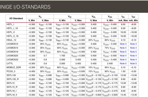
EINIGE I/O-STANDARDS Artix-7 FPGAs Data Sheet: DC and AC Switching Characteristics
Table 8:SelectIO DC Input and Output Levels
(1)(2)I/O Standard VIL VIH VOL VOH IOL IOH
V, Min V, Max V, Min V, Max V, Max V, Min mA, Max mA, Min
HSTL_I –0.300 VREF– 0.100 VREF+ 0.100 VCCO+ 0.300 0.400 VCCO– 0.400 8.00 –8.00 HSTL_I_18 –0.300 VREF– 0.100 VREF+ 0.100 VCCO+ 0.300 0.400 VCCO– 0.400 8.00 –8.00 HSTL_II –0.300 VREF– 0.100 VREF+ 0.100 VCCO+ 0.300 0.400 VCCO– 0.400 16.00 –16.00 HSTL_II_18 –0.300 VREF– 0.100 VREF+ 0.100 VCCO+ 0.300 0.400 VCCO– 0.400 16.00 –16.00 HSUL_12 –0.300 VREF– 0.130 VREF+ 0.130 VCCO+ 0.300 20% VCCO 80% VCCO 0.10 –0.10 LVCMOS12 –0.300 35% VCCO 65% VCCO VCCO+ 0.300 0.400 VCCO– 0.400 Note 3 Note 3 LVCMOS15 –0.300 35% VCCO 65% VCCO VCCO+ 0.300 25% VCCO 75% VCCO Note 4 Note 4 LVCMOS18 –0.300 35% VCCO 65% VCCO VCCO+ 0.300 0.450 VCCO– 0.450 Note 5 Note 5
LVCMOS25 –0.300 0.7 1.700 VCCO+ 0.300 0.400 VCCO– 0.400 Note 4 Note 4
LVCMOS33 –0.300 0.8 2.000 3.450 0.400 VCCO– 0.400 Note 4 Note 4
LVTTL –0.300 0.8 2.000 3.450 0.400 2.400 Note 5 Note 5
MOBILE_DDR –0.300 20% VCCO 80% VCCO VCCO+ 0.300 10% VCCO 90% VCCO 0.10 –0.10 PCI33_3 –0.400 30% VCCO 50% VCCO VCCO+ 0.500 10% VCCO 90% VCCO 1.50 –0.50 SSTL135 –0.300 VREF– 0.090 VREF+ 0.090 VCCO+ 0.300 VCCO/2 – 0.150 VCCO/2 + 0.150 13.00 –13.00 SSTL135_R –0.300 VREF– 0.090 VREF+ 0.090 VCCO+ 0.300 VCCO/2 – 0.150 VCCO/2 + 0.150 8.90 –8.90 SSTL15 –0.300 VREF– 0.100 VREF+ 0.100 VCCO+ 0.300 VCCO/2 – 0.175 VCCO/2 + 0.175 13.00 –13.00 SSTL15_R –0.300 VREF– 0.100 VREF+ 0.100 VCCO+ 0.300 VCCO/2 – 0.175 VCCO/2 + 0.175 8.90 –8.90 SSTL18_I –0.300 VREF– 0.125 VREF+ 0.125 VCCO+ 0.300 VCCO/2 – 0.470 VCCO/2 + 0.470 8.00 –8.00 SSTL18_II –0.300 VREF– 0.125 VREF+ 0.125 VCCO+ 0.300 VCCO/2 – 0.600 VCCO/2 + 0.600 13.40 –13.40 Notes:
1. Tested according to relevant specifications.
2. 3.3V and 2.5V standards are only supported in HR I/O banks.
3. Supported drive strengths of 4, 8, or 12 mA in HR I/O banks.
4. Supported drive strengths of 4, 8, 12, or 16 mA in HR I/O banks.
5. Supported drive strengths of 4, 8, 12, 16, or 24 mA in HR I/O banks.
6. For detailed interface specific DC voltage levels, see UG471: 7 Series FPGAs SelectIO Resources User Guide.
Table 9:
Differential SelectIO DC Input and Output Levels
I/O Standard VICM(1) VID(2) VOCM(3) VOD(4)
V, Min V, Typ V, Max V, Min V, Typ V, Max V, Min V, Typ V, Max V, Min V, Typ V, Max
BLVDS_25 0.300 1.200 1.425 0.100 – – – 1.250 – Note 5
MINI_LVDS_25 0.300 1.200 VCCAUX 0.200 0.400 0.600 1.000 1.200 1.400 0.300 0.450 0.600 PPDS_25 0.200 0.900 VCCAUX 0.100 0.250 0.400 0.500 0.950 1.400 0.100 0.250 0.400 RSDS_25 0.300 0.900 1.500 0.100 0.350 0.600 1.000 1.200 1.400 0.100 0.350 0.600 TMDS_33 2.700 2.965 3.230 0.150 0.675 1.200 VCCO–0.405 VCCO–0.300 VCCO–0.190 0.400 0.600 0.800 Notes:
1. VICM is the input common mode voltage.
2. VID is the input differential voltage (Q – Q).
3. VOCM is the output common mode voltage.
4. VOD is the output differential voltage (Q – Q).
5. VOD for BLVDS will vary significantly depending on topology and loading.
Quelle: Xilinx, DS181, Artix-7 FPGAs Data Sheet: DC and AC Switching Characteristics, Table 8
96
Notizen
Notizen
Constraints & Synthese
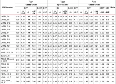
SWITCHING CHARACTERISTICS
DS181 (v1.18) March 18, 2015 www.xilinx.com
Product Specification 14
IOB Pad Input/Output/3-State
Table 17 summarizes the values of standard-specific data input delay adjustments, output delays terminating at pads (based on standard) and 3-state delays.
• TIOPI is described as the delay from IOB pad through the input buffer to the I-pin of an IOB pad. The delay varies depending on the capability of the SelectIO input buffer.
• TIOOP is described as the delay from the O pin to the IOB pad through the output buffer of an IOB pad. The delay varies depending on the capability of the SelectIO output buffer.
• TIOTP is described as the delay from the T pin to the IOB pad through the output buffer of an IOB pad, when 3-state is disabled. The delay varies depending on the SelectIO capability of the output buffer. In HR I/O banks, the IN_TERM termination turn-on time is always faster than TIOTP when the INTERMDISABLE pin is used.
Table 17:IOB High Range (HR) Switching Characteristics
I/O Standard
TIOPI TIOOP TIOTP
Units
Speed Grade Speed Grade Speed Grade
1.0V 0.95V 0.9V 1.0V 0.95V 0.9V 1.0V 0.95V 0.9V
-3 -2/
-2LE -1 -1Q/
-1M -1LI -2LE -3 -2/
-2LE -1 -1Q/
-1M -1LI -2LE -3 -2/
-2LE -1 -1Q/
-1M -1LI -2LE LVTTL_S4 1.26 1.34 1.41 1.53 1.41 1.58 3.80 3.93 4.18 4.18 4.18 4.41 3.82 3.96 4.20 4.20 4.20 4.05 ns LVTTL_S8 1.26 1.34 1.41 1.53 1.41 1.58 3.54 3.66 3.92 3.92 3.92 4.15 3.56 3.69 3.93 3.93 3.93 3.78 ns LVTTL_S12 1.26 1.34 1.41 1.53 1.41 1.58 3.52 3.65 3.90 3.90 3.90 4.13 3.54 3.68 3.91 3.91 3.91 3.77 ns LVTTL_S16 1.26 1.34 1.41 1.53 1.41 1.58 3.07 3.19 3.45 3.45 3.45 3.68 3.09 3.22 3.46 3.46 3.46 3.31 ns LVTTL_S24 1.26 1.34 1.41 1.53 1.41 1.58 3.29 3.41 3.67 3.67 3.67 3.90 3.31 3.44 3.68 3.68 3.68 3.53 ns LVTTL_F4 1.26 1.34 1.41 1.53 1.41 1.58 3.26 3.38 3.64 3.64 3.64 3.86 3.28 3.41 3.65 3.65 3.65 3.50 ns LVTTL_F8 1.26 1.34 1.41 1.53 1.41 1.58 2.74 2.87 3.12 3.12 3.12 3.35 2.76 2.90 3.13 3.13 3.13 2.99 ns LVTTL_F12 1.26 1.34 1.41 1.53 1.41 1.58 2.73 2.85 3.10 3.10 3.10 3.33 2.74 2.88 3.12 3.12 3.12 2.97 ns LVTTL_F16 1.26 1.34 1.41 1.53 1.41 1.58 2.56 2.68 2.93 2.93 2.93 3.16 2.57 2.71 2.95 2.95 2.95 2.80 ns LVTTL_F24 1.26 1.34 1.41 1.53 1.41 1.58 2.52 2.65 2.90 3.23 2.90 3.22 2.54 2.68 2.91 3.24 2.91 2.86 ns LVDS_25 0.73 0.81 0.88 0.89 0.88 0.90 1.29 1.41 1.67 1.67 1.67 1.86 1.31 1.44 1.68 1.68 1.68 1.50 ns MINI_LVDS_25 0.73 0.81 0.88 0.89 0.88 0.90 1.27 1.40 1.65 1.65 1.65 1.88 1.29 1.43 1.66 1.66 1.66 1.52 ns BLVDS_25 0.73 0.81 0.88 0.88 0.88 0.90 1.84 1.96 2.21 2.76 2.21 2.44 1.85 1.99 2.23 2.77 2.23 2.08 ns RSDS_25 (point
to point) 0.73 0.81 0.88 0.89 0.88 0.90 1.27 1.40 1.65 1.65 1.65 1.88 1.29 1.43 1.66 1.66 1.66 1.52 ns PPDS_25 0.73 0.81 0.88 0.89 0.88 0.90 1.29 1.41 1.67 1.67 1.67 1.88 1.31 1.44 1.68 1.68 1.68 1.52 ns TMDS_33 0.73 0.81 0.88 0.92 0.88 0.90 1.41 1.54 1.79 1.79 1.79 1.99 1.43 1.57 1.80 1.80 1.80 1.63 ns PCI33_3 1.24 1.32 1.39 1.52 1.39 1.57 3.10 3.22 3.48 3.48 3.48 3.71 3.12 3.25 3.49 3.49 3.49 3.34 ns HSUL_12_S 0.67 0.75 0.82 0.88 0.82 0.87 1.81 1.93 2.18 2.18 2.18 2.41 1.82 1.96 2.20 2.20 2.20 2.05 ns HSUL_12_F 0.67 0.75 0.82 0.88 0.82 0.87 1.29 1.41 1.67 1.67 1.67 1.90 1.31 1.44 1.68 1.68 1.68 1.53 ns DIFF_HSUL_
12_S 0.68 0.76 0.83 0.86 0.83 0.88 1.81 1.93 2.18 2.18 2.18 2.21 1.82 1.96 2.20 2.20 2.20 1.84 ns DIFF_HSUL_
12_F 0.68 0.76 0.83 0.86 0.83 0.88 1.29 1.41 1.67 1.67 1.67 1.79 1.31 1.44 1.68 1.68 1.68 1.42 ns MOBILE_
DDR_S 0.76 0.84 0.91 0.91 0.91 0.96 1.68 1.80 2.06 2.06 2.06 2.24 1.70 1.83 2.07 2.07 2.07 1.88 ns MOBILE_
DDR_F 0.76 0.84 0.91 0.91 0.91 0.96 1.38 1.51 1.76 1.76 1.76 1.97 1.40 1.54 1.77 1.77 1.77 1.61 ns DIFF_MOBILE_
DDR_S 0.70 0.78 0.85 0.85 0.85 0.87 1.70 1.82 2.07 2.07 2.07 2.24 1.71 1.85 2.09 2.09 2.09 1.88 ns DIFF_MOBILE_
DDR_F 0.70 0.78 0.85 0.85 0.85 0.87 1.45 1.57 1.82 1.82 1.82 2.00 1.46 1.60 1.84 1.84 1.84 1.64 ns
Quelle: Xilinx, DS181, Artix-7 FPGAs Data Sheet: DC and AC Switching Characteristics, Table17
97
Constraints & Synthese
CLOCKS
Für Timing-Analysen müssen Clock-Beschreibungen durch geeignete Constraints angelegt werden:
create_clock -period 10.000 -name clk -waveform {0.000 5.000}\
[get_ports clk100Mhz]
Dies beschreibt einen 100 MHz Takt mit einem Tastverhältnis von 50%, da alle Einheiten in ns gegeben werden.
0ns 5ns 10ns
clk100Mhz
15ns 50 %
50 %
Weitere Hinweise zum Umgang mit Clocks findet sich in UG903, Vivado Design Suite User Guide, Using Constraints
98
Notizen
Notizen
Constraints & Synthese
CLOCKS (II)
Auch andere Tastverhältnisse sind möglich:
create_clock -period 8.000 -name clk -waveform {2.000 8.000}\
[get_ports clk125Mhz]
0ns 2ns 10ns
clk125Mhz
16ns 25 % 75 %
8ns
Aus einem Taktsignal abgeleitete Takte werden von Vivado erkannt und entsprechend in die Timinganalyse übernommen.
Mit verschiedenen Primitiven auf einem FPGA können nahezu beliebige Takte erzeugt werden. Auf den verwendeten
Artix7-Bausteinen stehen z.B. Mixed-Mode Clock Manager (MMCM) zur Verfügung.
99
Constraints & Synthese
EIN MMCM
Notizen
Notizen
EIN MMCM (II)
Solche Clock Manager können mit dem „Clock-Wizard“ von Vivado instantiiert werden oder durch besondere VHDL-Beschreibungen, die das Synthesetool automatisch erkennt (siehe: UG768, Xilinx 7 Series FPGA Libraries Guide for HDL Designs)
1
library ieee;
2
use ieee.std_logic_1164.all;
3
4
library unisim;
5
use unisim.vcomponents.all;
6
7
entity ClkGen is
8
9
port (reset : in std_logic;
10
clkIn : in std_logic;
11
clkOut : out std_logic );
12
13
end ClkGen;
101
Constraints & Synthese
EIN MMCM (III)
Kleiner Ausschnitt:
1
-- Instantiate a input clock buffer
2
clkInBuffer : IBUFG
3
port map (O => clkInI ,
4
I => clkIn );
5
-- Instantiate a clock buffer for the internal feedback signal
6
feedbackBuffer : BUFG
7
port map (O => clkfbIBuf ,
8
I => clkfbI );
9
-- Instantiate a clock manager
10
clkgen : MMCME2_ADV
11
generic map (
12
CLKFBOUT_MULT_F => 8.000 , -- multiply feedback for 80Mhz
13
--CLKFBOUT_MULT_F => 10.000 , -- multiply feedback for 100 Mhz
14
CLKFBOUT_PHASE => 0.000 , -- phase of feedback output
15
CLKFBOUT_USE_FINE_PS => false , -- Don 't enable fine shift
16
...)
102