Mathematical Modeling of Semiconductor Devices
Prof. Dr. Ansgar J¨ ungel Fachbereich Mathematik und Statistik
Universit¨at Konstanz Preliminary version
Contents
1 Introduction 3
2 Some Semiconductor Physics 11
2.1 Semiconductor crystals . . . 11
2.2 Mean electron velocity and effective mass approximation . . . 17
2.3 Semiconductor statistics . . . 21
3 Classical Kinetic Transport Models 27 3.1 The Liouville equation . . . 27
3.2 The Vlasov equation . . . 31
3.3 The Boltzmann equation . . . 37
3.4 Extensions . . . 44
4 Quantum Kinetic Transport Equations 50 4.1 The Wigner equation . . . 50
4.2 The quantum Vlasov and quantum Boltzmann equation . . . 56
5 From Kinetic to Fluiddynamical Models 62 5.1 The drift-diffusion equations: first derivation . . . 62
5.2 The drift-diffusion equations: second derivation . . . 74
5.3 The hydrodynamic equations . . . 76
5.4 The Spherical Harmonic Expansion (SHE) model . . . 80
5.5 The energy-transport equations . . . 92
5.6 Relaxation-time limits . . . 100
5.7 The extended hydrodynamic model . . . 104
6 The Drift-Diffusion Equations 114
6.1 Thermal equilibrium state and boundary conditions . . . 114
6.2 Scaling of the equations . . . 116
6.3 Static current-voltage characteristic of a diode . . . 118
6.4 Numerical discretization of the stationary equations . . . 127
7 The Energy-Transport Equations 131 7.1 Symmetrization and entropy . . . 132
7.2 A drift-diffusion formulation . . . 136
7.3 A non-parabolic band approximation . . . 140
8 From Kinetic to Quantum Hydrodynamic Models 143 8.1 The quantum hydrodynamic equations: first derivation . . . 143
8.2 The quantum hydrodynamic equations: second derivation . . . 147
8.3 Extensions . . . 153
1 Introduction
The modern computer and telecommunication industry relies heavily on the use and development of semiconductor devices. Since the first semiconductor device (a germanium transistor) has been built by Bardeen, Brattain and Shockley in 1947, a lot of different devices for special applications have been invented in the following decades. A very important fact of the success of semiconductor devices is that the device length is very small compared to previous electronic devices (like tube transistors). The first transistor of Bardeen, Brattain and Shockley had a characteristic length (the emitter-collector length) of 20µm. Thanks to the progressive miniaturization of semiconductor devices, the transistors in a modern Pentium IV processor have a characteristic length of 0.18µm. The device length of tunneling diodes, produced in laboratories, is only of the order of 0.075µm.
Nowadays, semiconductor materials are contained in almost all electronic de- vices. Some examples of semiconductor devices and their use are described in the following.
• Photonic devices capture light (photons) and convert it into an electronic signal. They are used in camcorders, solar cells, and light-wave communi- cation systems as optical fibers.
• Optoelectronic emitters convert an electronic signal into light. Examples are light-emitting diodes (LED) used in displays and indication lambs and semiconductor lasers used in compact disk systems, laser printers, and eye surgery.
• Flat-panel displays create an image by controlling light that either passes through the device or is reflected off of it. They are made, for instance, of liquid crystals (liquid-crystal displays, LCD) or of thin semiconductor films (electroluminescent displays).
• Infield-effect devices the conductivity is modulated by applying an electric field to a gate contact on the surface of the device. The most important field-effect device is the MOSFET (metal-oxide semiconductor field-effect transistor), used as a switch or an amplifier. Integrated circuits are mainly made of MOSFETs.
• Quantum devices are based on quantum mechanical phenomena, like tun- neling of electrons through potential barriers which are impenetrable clas- sically. Examples are resonant tunneling diodes, superlattices (multi-quan- tum-well structures), quantum wires in which the motion of carriers is re- stricted to one space dimension and confined quantum mechanically in the other two directions, and quantum dots.
Clearly, there are many other semiconductor devices which are not mentioned (for instance, bipolar transistors, Schottky barrier diodes, thyristors). Other new developments are, for instance, nanostructure devices (heterostructures) and solar cells made of amorphous silicon or organic semiconductor materials (see [14, 41]).
Usually, a semiconductor device can be considered as a device which needs an input (an electronic signal or light) and produces an output (light or an electronic signal). The device is connected to the outside world by contacts at which a voltage (potential difference) is applied. We are mainly interested in devices which produce an electronic signal, for instance the macroscopically measurable electric current (electron flow), generated by the applied bias. In this situation, the input parameter is the applied voltage and the output parameter is the electric current through one contact. The relation between these two physical quantities is calledcurrent-voltage characteristic. It is a curve in the two-dimensional current- voltage space. The current-voltage characteristic does not need to be a monotone function and it does not need to be a function (but a relation).
The main objective of this book is to derive mathematical models which de- scribe the electron flow through a semiconductor device due to the application of a voltage. Depending on the device structure, the main transport phenomena of the electrons may be very different, for instance, due to drift, diffusion, convec- tion, or quantum mechanical effects. For this reason, we have to devisedifferent mathematical models which are able to describe the main physical phenomena for a particular situation or for a particular device.
This leads to ahierarchyof semiconductor models. Roughly speaking, we can divide semiconductor models in three classes: quantum models, kinetic models and fluiddynamical (macroscopic) models. In order to give some flavor of these models and the methods used to derive them, we explain these three view-points:
quantum, kinetic and fluiddynamic in a simplified situation.
The quantum view. Consider a single electron of mass m and elementary charge q moving in a vacuum under the action of an electric field E = E(x, t).
The motion of the electron in space x ∈ Rd and time t > 0 is governed by the single-particle Schr¨odinger equation
i~∂tΨ = −~2
2m∆Ψ−qV(x, t)Ψ, x∈Rd, t >0, (1.1) with some initial condition
Ψ(x,0) = Ψ0(x), x∈Rd. (1.2) Here ~ = h/2π is the reduced Planck constant, V(x, t) the real-valued electro- static potential related to the electric field by E = −∇V, and i2 = −1. Any solution Ψ of (1.1)-(1.2) is called wave function. Macroscopic variables are ob-
tained by the definitions:
electron density: n =|Ψ|2, electron current density: J =−~q
mIm(Ψ∇Ψ),
where Ψ is the complex conjugate of Ψ. More precisely, n(x, t) is the position probability density of the particle, i.e.
Z
A
n(x, t)dx
is the probability to find the electron in the subset A⊂Rd at the time t.
Without too much exageration we can say that all other descriptions for the evolution of the electron, and in particular the fluiddynamical and kinetic models, can be derived from the Schr¨odinger equation (1.1).
The fluiddynamical view. In order to derive fluiddynamical models, for instance, for the evolution of the particle densitynand the current density J, we assume that the wave function can be decomposed in its amplitude √
n(x, t)>0 and phase S(x, t)∈R:
Ψ =√
neimS/~. (1.3)
This expression makes sense as long as the electron density stays positive. We call this change of unknowns Ψ 7→ (n, S) Madelung transform. The current density now reads
J =−~q mIm
·√ n
µ ∇n 2√
n +im
~
√n∇S
¶¸
=−qn∇S,
and we can interpret S also as a velocity potential. Setting (1.3) into the Schr¨odinger equation (1.1) and taking the imaginary and real part of the re- sulting equation, gives, after some computations (see Chapter 8):
∂tn− 1
qdivJ = 0, (1.4)
∂tJ −1 qdiv
µJ⊗J n
+ ~2q 2m2n∇
µ∆√
√ n n
− q2
mnE = 0. (1.5) Here, J⊗J is a tensor (or matrix) with components JjJk, where j, k= 1, . . . , d.
Equation (1.4) expresses the conversation of mass. Indeed, d
dt Z
Rdn dx= 1 q
Z
RddivJ dx= 0.
The equations (1.4)-(1.5) are referred to as thequantum hydrodynamic equations.
They are equivalent to the Schr¨odinger equation (1.1) as long as n > 0. If they are studied in the whole space, the initial conditions
n(·,0) =|Ψ0|2, J(·,0) =−~q
mIm(Ψ0∇Ψ0) inRd
have to be prescribed.
In the semi-classical limit “~ →0” the equations (1.4)-(1.5) formally reduce to thehydrodynamic equations
∂tn− 1
qdivJ = 0, (1.6)
∂tJ− 1 qdiv
µJ ⊗J n
− q2
mnE = 0, (1.7)
which are the Euler equations for a gas of charged particles with zero temperature in a given electric field. Clearly, the limit “~ → 0” does not make sense since
~ is a constant. After a scaling which makes the variables non-dimensional, a parameter (the so-called scaled Planck constant) appears in front of the scaled quantum term in (1.5). This parameter is small compared to one in certain physical ranges, for instance, when the characteristic length is “large” (compared to some reference length). Thus, the limit “~→0” has always to be understood as the limit of vanishing scaled Planck constant.
The fluiddynamical formulation has some advantages:
• The equations are already formulated for macroscopic quantities.
• If the equations are considered in bounded domains (which is natural when dealing with semiconductor devices), boundary conditions can be more eas- ily prescribed compared to the Schr¨odinger formulation.
• In two or three space dimensions, fluiddynamical models are usually nu- merically cheaper than the Schr¨odinger equation.
The kinetic view. We start again with the Schr¨odinger equation (1.1).
First, introduce the so-called density matrix
ρ(r, s, t) = Ψ(r, t)Ψ(s, t), r, s∈Rd, t >0, and make the change of coordinates
r=x+ ~
2mη, s=x− ~ 2mη in the density matrix defining
u(x, η, t) =ρ³
x+ ~
2mη, x− ~ 2mη, t´
.
Since (~/2m)ηhas the dimension of length and~/2mhas the dimension ofm2/s, η has the dimension of inverse velocity. We prefer to work with the variables space, velocity and time instead of space, inverse velocity and time and employ
therefore the Fourier transformation to u. We recall that the Fourier transform F is defined by
F g(η) = ˆg(η) = (2π)−d/2 Z
Rdg(η)e−iη·v dv for (sufficiently smooth) functionsg :Rd→C with inverse
F−1h(v) = ˇh(v) = (2π)−d/2 Z
Rdh(v)eiη·v dη
forh:Rd →C. The inverse Fourier transform of u is called Wigner function w:
w= (2π)−d/2F−1u= (2π)−d/2u.ˇ
This function was introduced by Wigner in 1932 [43]. It can be shown (see Chapter 4) that the macroscopic electron densitynand current densityJ defined above in terms of the wave function can now be written in terms of the Wigner function as
n(x, t) = Z
Rdw(x, v, t)dv, (1.8)
J(x, t) = −q Z
Rdv w(x, v, t)dv. (1.9) The integrals are called the zeroth-order and first-order moments.
The transport equation forw is obtained by first deriving the evolution equa- tion for u from the Schr¨odinger equation (1.1) and then by taking the inverse Fourier transform of the equation for u. A computation leads to the so-called Wigner equation (see Chapter 4 for details):
∂tw+v· ∇xw+ q
mθ[V]w= 0, x, v ∈Rd, t >0, (1.10) where
(θ[V]w)(x, v, t) = im
~(2π)d Z
Rd
Z
Rd
· V
µ x+ ~
2mη, t
−V µ
x− ~ 2mη, t
¶¸
×w(x, v0, t)eiη·(v−v0) dv0 dη.
The initial condition forw reads w(x, v,0) = (2π)−d/2u(x, v,ˇ 0)
= (2π)−d Z
RdΨ0
µ
x+ ~ 2mη
¶ Ψ0
µ
x− ~ 2mη
eiv·η dη, x, v ∈Rd.
An operator, whose Fourier transform acts as a multiplication operator on the Fourier transform of the function, is called a linear pseudo-differential operator [42]. Since
θ[V\]w(x, η, t) = im
~
· V
µ
x+ ~ 2mη, t
−V µ
x− ~ 2mη, t
¶¸
ˆ
w(x, η, t), the operatorθ[V] is a pseudo-differential operator and the Wigner equation (1.10) is a linear pseudo-differential equation.
In the formal limit “~→0” it holds m
~
· V
µ
x+ ~ 2mη, t
−V µ
x− ~ 2mη, t
¶¸
→ ∇xV(x, t)·η, and using the identity i(ηu)∨ =∇vu,ˇ we obtain, as “~→0”,
θ[v]w→ i
(2π)d/2(∇xV ·ηu)∨ = 1
(2π)d/2∇xV · ∇vuˇ=∇xV · ∇vw.
Hence the Wigner equation becomes in the semi-classical limit
∂tw+v · ∇xw+ q
m∇xV · ∇vw= 0. (1.11) This equation is called Liouville equation. It has to be solved in the position- velocity space (x, v) ∈ Rd ×Rd for times t > 0, supplemented with the initial condition
w(x, v,0) = (2π)−d/2lim
~→0u(x, v,ˇ 0)
= 1
(2π)d lim
~→0
Z
RdΨ0
µ
x+ ~ 2mη
¶ Ψ0
µ
x− ~ 2mη
eiv·η dη, x, v∈Rd. Clearly, the above limits have to be understood in a formal way.
From the solutionwof the kinetic Liouville equation, the macroscopic electron density n and current density J are computed as in the quantum case by the formulas (1.8)-(1.9).
The kinetic formulation of the motion of the electron seems much more com- plicate than the Schr¨odinger formulation since we pass from d+ 1 variables (d for the space and one for the time) to 2d+ 1 variables (d for the space, d for the velocity and one for the time). However, this formulation has the following advantages:
• In the case of an electron ensemble with many particles, an approximate formulation in the position-velocity space is possible (leading to the Vlasov equation; see Chapter 3). This means that the kinetic equation has to be solved in 2d+ 1 variables instead of M d+ 1 variables in the Schr¨odinger formulation, where M À1 is the number of particles.
• Short-range interactions of the particles (collisions) can be easily included in the classical kinetic models.
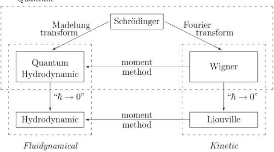
We have described how fluiddynamical and kinetic models can be derived formally from the Schr¨odinger equation. Is there any relation between fluiddy- namical and kinetic models? The answer is yes, and the method to see this is calledmoment method. In the following, we describe the idea of this method.
We start with the Liouville equation (1.11). Integrating (1.11) over the veloc- ity space and using the definitions of the first two moments (1.8)-(1.9) and the divergence theorem gives forE =−∇V
0 = ∂t
Z
Rdw dv+ Xd
k=1
Z
Rdvk
∂w
∂xk
dv− q m
Xd k=1
Ek
Z
Rd
∂w
∂vk
dv
= ∂tn− 1 qdivxJ,
which equals (1.6) expressing the conservation of mass. Now we multiply (1.11) with −qvj and integrate over the velocity space:
0 = ∂tJj−q Xd k=1
Z
Rdvjvk∂w
∂xk
dv+ q2 m
Xd k=1
Ek Z
Rdvj∂w
∂vk
dv
= ∂tJj−q Xd k=1
∂
∂xk
Z
Rdvjvkw dv− q2 m
Xd k=1
Ek
Z
Rd
∂vj
∂vk
w dv.
Since∂vj/∂vk =δjk with the Kronecker symbolδjk,this yields
∂tJ−qdivx
Z
Rd(v⊗v)w dv− q2
mEn= 0. (1.12)
The term Z
Rd(v⊗v)w dv
is the matrix of all second-order moments and is called energy tensor. We make now the complete heuristic assumption that the velocityv can be approximated by an average velocity
¯ v =
R vw dv
R w dv =−J qn, that means, Z
R(v⊗v)w dv≈(¯v⊗v)¯ Z
Rdw dv= 1 q2
J⊗J n ,
and (1.12) becomes
∂tJ −1 qdivx
µJ⊗J n
− q2
mnE = 0,
which equals (1.7). Under the above approximation, we have derived the hy- drodynamic model (1.6)-(1.7). For a more general derivation (including thermal effects), see Chapter 5.
In a similar way, we can apply the moment method to the Wigner equa- tion (1.10) in order to derive the quantum hydrodynamic model (1.4)-(1.5) (see Chapter 8).
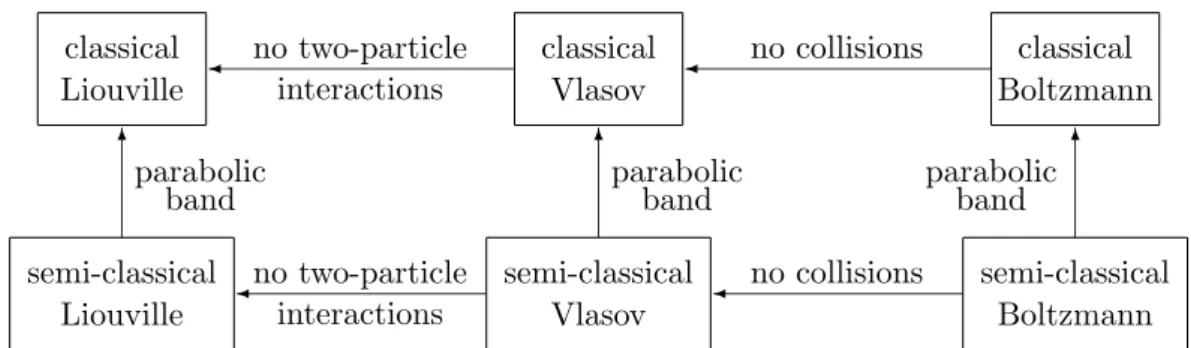
All the models explained in this chapter and the relations between them are summarized in Figure 1.1.
Fluidynamical Hydrodynamic
Quantum Hydrodynamic
?
“~→0”
Kinetic Liouville
¾ moment
method
Wigner
?
“~→0”
¾ moment
method Schr¨odinger
©©
©©
©©
©©
¼
HHHH
HHHHj
Madelung
transform Fourier
transform Quantum
Figure 1.1: Models for the motion of an electron in a vaccum.
The above models are all derived in a very simplified situation. For the modeling of the electron flow in semiconductors we have to take into account:
• the description of the motion of many particles;
• the influence of the semiconductor crystal lattice;
• two-particle long-range interactions (Coulomb force between the electrons);
• two-particle short-range interactions (collisions of the particles with the crystal lattice or with other particles).
These features will be included in our models step by step in the following chap- ters.
2 Some Semiconductor Physics
In this chapter we present a short summary of the physics and main properties of semiconductors. Only these subjects relevant to the subsequent chapters are included here. We refer to [1, 8, 14, 28, 41] for a detailed description of solid-state and semiconductor physics.
2.1 Semiconductor crystals
What is a semiconductor? Historically, the term semiconductor has been used to denote solid materials with a much higher conductivity than insulators, but a much lower conductivity than metals measured at room temperature. A more precise definition is that a semiconductor is a solid with anenergy gaplarger than zero and smaller than about 4 eV. Metals have no energy gap, whereas this gap is usually larger than 4 eV in insulators. In order to understand what an energy gap is, we have to explain the crystal structure of solids.
A solid is made of an infinite three-dimensional array of atoms arranged ac- cording to a lattice
L={` ~a1+m ~a2+n ~a3 : `, m, n∈Z} ⊂R3,
wherea~1, ~a2, ~a3 are the basis vectors of L, usually called primitive vectorsof the lattice. The lattice atoms (or ions) generate a periodic electrostatic potentialVL:
VL(x+y) =VL(x) ∀x∈R3, y ∈L.
The state of an electron moving in this periodic potential is described by an eigenfunction of the stationary Schr¨odinger equation:
−~2
2m∆Ψ−qVL(x)Ψ =εΨ, x∈R3, (2.1) where Ψ :R3 →Cis called wave function. In this equation, the physical param- eters are the reduced Planck constant ~ =h/2π, the electron mass (at rest) m, the elementary charge q, and the total energy ε. In fact, (2.1) is an eigenvalue problem, and we have to find eigenfunction-eigenvalue pairs (Ψ, ε). We consider two examples.
Example 2.1 (Free electron motion)
First, consider a free electron moving in a one-dimensional vacuum, i.e.,VL(x) = 0 for all x∈R.Then the solutions of (2.1) are given by
Ψk(x) =Aeikx+Be−ikx, x∈R, and
ε = ~2k2 2m ,
for anyk ∈R.We disregard purely imaginary values ofk =iγ (γ ∈R) which also yield real values of the energy, since this leads to unbounded solutions of the type exp(±ikx) = exp(∓γx) for x ∈ R. (Notice that the integral of |Ψ|2 over R can be interpreted as the particle mass which should be finite.) Thus the eigenvalue problem (2.1) has infinitely many solutions corresponding to different energies.
The functions exp(±ikx) are calledplane waves.
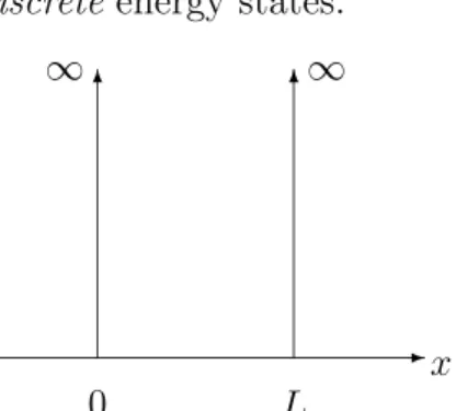
Example 2.2 (Infinite square-well potential)
The infinite square-well potential is a one-dimensional structure in which the potential is infinite at the boundaries and everywhere outside and zero everywhere within. As the potential is confining an electron to the inner region, we have to solve the Schr¨odinger equation (2.1) in the interval (0, L) of length L > 0 with boundary conditions
Ψ(0) = Ψ(L) = 0
and potential VL(x) = 0 for x ∈ (0, L) (see Figure 2.1). The eigenfunctions of (2.1) are given by
Ψk(x) =Aksin(kx), x∈(0, L), with discrete eigenvalues k=πn/L, n∈N, and energies
ε(k) = ~2k2
2m , k = πn L . The system only allows discreteenergy states.
-x
0 L
∞ 6 6∞
Figure 2.1: Infinite square-well potential.
Although the lattice potential VL is periodic, the wave function is defined on R3 in order to account for electron motion from one lattice cell to the next. In fact, the so-called Bloch theorem states that the Schr¨odinger equation (2.1) can be reduced to a Schr¨odinger equation on a so-called primitive cell of the lattice.
Before we state the result, we need some definitions.
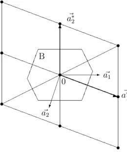
Definition 2.3 (1) The reciprocal lattice L∗ corresponding to L is defined by L∗ ={` ~a∗1+m ~a∗2 +n ~a∗3 : `, m, n∈Z},
where the basis vectors (or primitive vectors) a~∗1, ~a∗2, ~a∗3 ∈ R3 satisfy the relation
~
am·a~∗n = 2πδmn.
(2) The connected set D ⊂ R3 is called primitive cell of L (or of L∗) if and only if
• the volume ofD equals the volume of the parallelepiped spanned by the basis vectors of L (or of L∗);
• the whole space R3 is covered by the union of translates of D by the primitive vectors.
(3) The (first) Brillouin zone B ⊂ R3 is that primitive cell of the reciprocal latticeL∗ which consists of those points, which are closer to the origin than to any other point of L∗ (see Figure 2.2).
aaaaaa
aaaaaa
aaaaa
aa aa aa aa aa aa aa aa
a©©©©©©©©©©©©©©©©©
¯¯A¯A¯A¯ A
¯¯
¯¯
¯A AA
A aaaaaa
aaaaaa
aaaaa s
s s
s
s
s
s s
s - a~1
££
££°£
0
a~∗1
~ a2
a~∗2
B
aaaaaa aaaq 6
Figure 2.2: The primitive vectors of a two-dimensional latticeLand its reciprocal latticeL∗ and the Brillouin zone B.
We give some explainations of the above definition. As the wave planes exp(±ik ·x) suggest, k can be considered as a reciprocal variable which leads to the definitions of the reciprocal lattice and the Brillouin zone. In particular, for any x∈L and k ∈L∗ with
x= X3 m=1
αm~am and k = X3 n=1
βn~a∗n, αm, βn∈Z,
we obtain
exp(ik·x) = exp Ã
i X3 m,n=1
αmβn·2πδmn
!
= exp Ã
2πi X3 n=1
αnβn
!
= 1.
As x has the dimension of length, k has the dimension of inverse length and therefore, k is called a wave vector. (More precisely, k is called pseudo-wave vector; see below.)
The Brillouin zone can be constructed as follows. Draw arrows from a lattice point to its nearest neighbors and cut them in half. The planes through these intermediate points perpendicular to the arrows form the surface of the (bounded) Brillouin zone. In two space dimensions, the Brillouin zone is always a hexagon (or a square; see Figure 2.2).
Now we are able to apply the Bloch theorem. It says that the Schr¨odinger equation (2.1) is equivalent to the system of Schr¨odinger equations
−~2
2m∆Ψk−qVLΨk =ε(k)Ψk, x∈D, (2.2) indexed by k ∈B, with pseudo-periodic boundary conditions
Ψk(x+y) = Ψk(x)eik·y forx, x+y∈∂D, (2.3) where D is a primitive cell of L. (This follows from the fact that the Hamilton operatorH =−(~2/2m)∆ +qVL(x) commutes with all the translation operators T` associated with the lattice, where (T`Ψ)(x) = Ψ(x+`) for ` ∈L, x∈R3.) By functional analysis, the eigenvalue problem (2.2)-(2.3), for any k ∈ B, possesses a sequence of eigenfunctions Ψnk with associated eigenvalues εn(k), n ∈ N0. The relation between Ψk and Ψ is given by
Ψk(x) =X
`∈L
e−ik·`Ψ(x+`).
We can also write Ψnk as distorted waves
Ψnk(x) =unk(x)eik·x, (2.4) where
unk(x) = X
`∈L
e−ik·(x+`)Ψ(x+`)
is clearly periodic inL. In some sense, Ψnk are plane waves which are modulated by a periodic functionunk taking into account the influence of the lattice of atoms.
The functions (2.4) are also calledBloch functions. Since the vectork appears in distorted plane waves, it is not termed wave vector but pseudo-wave vector.
The function k 7→ εn(k) is called the disperson relation or the n-th energy band. It shows how the energy of the n-th band depends on the wave vector
k. The union of the ranges of εn over n ∈ N is not necessarily the whole set R, i.e., there may exist energies ε∗ for which there is no n ∈ N and no k ∈ B such thatεn(k) =ε∗.The connected components of the set of energies with this non-existence property are calledenergy gaps. We illustrate this property by an example.
Example 2.4 (Kronig-Penney model)
We study a simple one-dimensional model for the periodic potential generated by the lattice atoms. We use the square-well potential (see Figure 2.3)
VL(x) =
½ V0 : −b < x≤0 0 : 0< x≤a, and VL is extended to R with perioda+b, i.e.
VL(x) = VL(x+a+b) ∀x∈R, wherea, b >0 and V0 ∈R.
- 6
−b 0 V0
a a+b VL(x)
x Figure 2.3: Periodic square-well potential VL.
In order to solve the Schr¨odinger equation (2.1), we make the Bloch ansatz Ψk(x) =u(x)eikx
with an (a+b)-periodic function u.Set α=
r2mε
~2 , β =
r2m(ε−qV0)
~2 .
If ε < qV0 then β can be written as β = iγ with γ > 0. A computation shows that the general solution of (2.1) in the interval (−b, a) is given by
u(x) =
½ Aei(α−k)x+Be−i(α+k)x : 0< x≤a Cei(β−k)x+De−i(β+k)x : −b < x ≤0.
The constantsA,B,C andD can be determined from the boundary conditions.
More precisely, we assume thatuis continuously differentiable and periodic in R: u(a+ 0) =u(a−0), u(a+ 0) =u(a−0),
u(−b) = u(a), u0(−b) = u0(a),
where u(a+ 0) = limx&au(x) etc. This gives four linear equations for the four unknows A, B, C and D. They can be casted into a linear system
M(A, B, C, D)>= 0
with matrix M ∈ C4×4. (The sign “>” means the transposed of a vector.) The necessary conditions for getting non-trivial solutions is that detM = 0. An ele- mentary, but lenghty calculation shows that this conditon is equivalent to
cos(k(a+b)) = s
1 +
µα2−β2 2αβ
¶2
sin2(βb)·cos(αa−δ), (2.5) where
tanδ =−α2+β2
2αβ tan(βb).
The equation (2.5) is implicit in k and real-valued for all values of the energy.
Indeed, if ε > qV0 we have β = iγ and sin(βb)/β = sinh(γb)/γ since sin(ix) = isinh(x).
The right-hand side of (2.5) may be larger than +1 or smaller than −1 for certain values ofε.Then (2.5) is solvable only for imaginary wave vectorsk =iκ, κ ∈ R. But then Ψ(x) = u(x) exp(ikx) = u(x) exp(−κx) and this gives non- integrable solutions inR.We conclude that there exist values ofεfor which (2.5) has no real solution k. Every connected subset of [0,∞)\R(ε), where R(ε) = {ε0 ∈[0,∞) : ∃k∈R: ε(k) =ε0},is an energy gap.
In Table 2.1 some values of energy gaps for some semiconductor materials are collected. The energy gap separates two energy bands. The nearest energy band
Material Energy gap εg (eV)
Silicon 1.12
Germanium 0.664
Gallium-Arsenide 1.424
Table 2.1: Energy gaps of selected semiconductors.
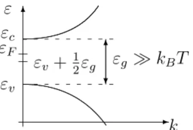
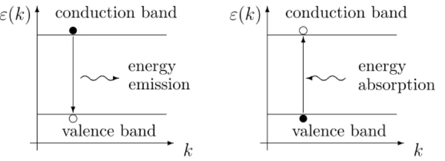
below the energy gap is called valence band; the nearest energy band above the energy gap is termed conductor band (see Figure 2.4).
Now we are able to state the definition of asemiconductor: It is a solid with an energy gap whose value is positive and smaller than about 4 eV.
- 6
6?
εg ε
k
valence band conduction band
Figure 2.4: Schematic band structure with energy gap εg.
2.2 Mean electron velocity and effective mass approxima- tion
In this section we will motivate the following two expressions:
• The mean electron velocity (or group velocity of the wave packet) in the n-th band is given by
vn(k) = 1
~∇kεn. (2.6)
• The effective mass tensorm∗ is defined by (m∗)−1 = 1
~2 d2εn
dk2 . (2.7)
Motivation of (2.6). The result (2.6) can be obtained as follows. We omit in the following the index n and define the group velocity by
v(k) = µZ
D|Ψ|2 dx
¶−1Z
D
ˆ
vk|Ψk|2 dx,
whereD is a primitive cell of the lattice and ˆvk is the particle velocity ˆ
vk =− Jk
qnk
= ~ m
Im(Ψk∇xΨk)
|Ψk|2 . (2.8)
In order to show (2.6) we have to compute the integral Z
D
Im(Ψk∇xΨk)dx.
We take the derivative of (2.2) with respect to k,use the distorted wave plane Ψk(x) = uk(x)eik·x
and
∆x(∇kΨk) = ∆x
¡eik·x∇kuk+ixΨk
¢
= ∆x
¡eik·x∇kuk
¢+ 2i∇xΨk+ix∆xΨk
to obtain
(∇kε)Ψk = −~2
2m∆x(∇kΨk)−(qVL+ε)∇kΨk
= µ
− ~2
2m∆x−(qVL+ε)
(eik·x∇kuk+ixΨk)
= µ
− ~2
2m∆x−(qVL+ε)
(eik·x∇kuk) +ix µ
−~2
2m∆x−(qVL+ε)
¶ Ψk
−i~2 m∇xΨk
= µ
− ~2
2m∆x−(qVL+ε)
(eik·x∇kuk)−i~2
m∇xΨk.
Multiplying this equation by Ψk, integrating over D and integrating by parts yields
∇kε Z
D|Ψk|2 dx+i~2 m
Z
D
(∇xΨk)Ψkdx
= Z
D
eikx∇kuk
µ
−~2
2m∆x−qVL−ε
Ψk dx= 0, using (2.2) again. Thus
∇kε=−i~2R
D(∇xΨk)Ψkdx mR
D|Ψk|2dx . Taking the real part of both sides of this equation gives
∇kε= ~2 m
ImR
D(∇xΨk)Ψk dx R
D|Ψk|2dx =~v(k), which shows (2.6).
The expression (2.6) has some consequences. The change of energy with respect to time equals the product of force F and velocity vn:
∂tεn(k) = F vn(k) =~−1F∇kεn(k).
By the chain rule,
∂tεn(k) =∇kεn(k)∂tk and hence
F =∂t(~k). (2.9)
Newton law’s states that the force equals the time derivative of the momentum p.This motivates the definition of the crystal momentum
p=~k.
Motivation of (2.7). Another consequence follows from (2.6) and (2.9):
Differentiating (2.6) leads to
∂tvn = 1
~ d2εn
dk2 ∂tk= 1
~2 d2εn
dk2 F.
The momentum equals m∗vn, where m∗ is the (effective) mass. Using again Newton’s law F =∂tp=m∗∂tvn we obtain
(m∗)−1 = 1
~2 d2εn
dk2 .
We consider this equation as a definition of the effective mass m∗. The second derivative ofεn with respect tok is a 3×3 matrix, so thesymbol(m∗)−1 is also a matrix. If we evaluate the Hessian ofεnnear a local minimum, i.e. ∇kεn(k0) = 0, thend2εn(k0)/dk2 is a symmetric positive matrix which can be diagonalized and the diagonal elements are positive:
1/m∗x 0 0 0 1/m∗y 0
0 0 1/m∗z
= 1
~2 d2εn
dk2 (k0). (2.10) Assume that the energy values are shifted in such a way that the energy vanishes at the local minimumk0.For wave vectorsk “close” tok0,we have from Taylor’s formula and (2.10)
εn(k) = εn(k0) +∇kεn(k0)·k+1
2k>d2εn
dk2 (k0)k+O(|k−k0|3)
= ~2 2
µkx2 m∗x + k2y
m∗y + k2z m∗z
+O(|k−k0|3),
where k = (kx, ky, kz)>. If the effective masses are equal in all directions, i.e.
m∗ =m∗x =m∗y =m∗z,we can write, neglecting higher-order terms, εn(k) = ~2
2m∗|k|2 (2.11)
for wave vectorsk“close” to a local band minimum. In this situation,m∗is called the isotropic effective mass. We conclude that the energy of an electron near a band minimum equals the energy of a free electron in vacuum (see Example 2.1) where the (rest) mass of the electron is replaced by the effective mass. The effects of the crystal potential are represented by the effective mass.
The expression (2.11) is referred to as the parabolic band approximation and usually, the range of wave vectorskis extended to the whole space, i.e., k=R3 is assumed. In order to account for non-parabolic effects, the followingnon-parabolic band approximation in the sense of Kane is used [41, Ch. 2.1]:
εn(1 +αεn) = ~2|k|2 2m∗ ,
where α > 0 is a non-parabolicity parameter. In silicon, for instance, α = 0.5 (eV)−1.
Definition of holes. When we consider the effective mass near a band maximum, we find that the Hessian of εn is negative definite which would lead to a negative effective mass. However, in the derivation of the mean velocity and consequently, of the effective mass definition, we have used in (2.8) that the charge of the electrons is negative. Using a positive charge leads to a positive effective mass. The corresponding particles are calles holes. Physically, a hole is a vacant orbital in an otherwise filled (valence) band. Thus, the current flow in a semiconductor crystal comes from two sources: the flow of electrons in the conduction band and the flow of holes in the valence band. It is a convention to consider rather the motion of the valence band vacancies that the motion of the electrons moving from one vacant orbital to the next (Figure 2.5).
t= 0 :
ÁÀ ¿
s s
crystal atom£
££±
electron JJ^
ÁÀ ¿
c s R
orbital
À
¤¤¤º vacancy
t >0 :
ÁÀ ¿
s c vacancy
JJ^
ÁÀ ¿
s s
¤¤¤º electron
Figure 2.5: Motion of a valence band electron to a neighboring vacant orbital or, equivalently, motion of a hole in the inverse direction.
Semi-classical picture. In the so-called semi-classical picture, the motion of an electron in then-th band can be approximately described by a point particle moving with the velocity vn(k). Denoting by (x(t), vn(k, t)) the trajectory of an electron in the position-velocity phase space, we obtain from Newton’s law (see (2.9))
∂tx=vn(k) = 1
~∇kεn, ~∂tk =F, (2.12) whereF represents a driving force, for instance, F =−q∇xVL(x, t). Notice that band transitions are excluded since the band index n is fixed in the equations.
Non-periodic potentials. If a non-periodic potential (or driving force) is superimposed to VL, the Schr¨odinger equation (2.1) cannot be decomposed into the decoupled Schr¨odinger equations (2.2), and the above computations are no longer valid. In fact, the energy bands are now coupled. However, it is usually assumed that the non-periodic potential is so weak that the coupling of the bands can be neglected and then, the above analysis remains approximately valid.
2.3 Semiconductor statistics
Number densities. We want to determine the number of electrons in the conduction band and the number of holes in the valence band per unit volume.
In view of the very high number of particles (typically > 109cm−3) it seems appropriate to use statistical methods. We make the following assumptions:
• Electrons cannot be distinguished from one another.
• The Pauli exclusion principle holds, i.e., each level of a band can be occupied by not more than two electrons with opposite spin.
First we compute the number of possible states within all energy bands per unit volume (2π)3. In the continuum limit, this number equals:
g(ε) = 2 (2π)3
X
ν
Z
B
δ(ε−εν(k))dk. (2.13) The function g(ε) is called density of states. The factor 2 comes from the two possible states of the spin of an electron. The set B is the Brillouin zone (see Section 2.1), and the functionδ is the delta distribution defined by
Z ∞
−∞
δ(ε0 −ε)φ(ε)dε=φ(ε0) (2.14) for all appropriate functions φ. Mathematically, δ is a functional operating in some function space and the above integral has to be interpreted as the value of δ(ε0−ε) acting on φ(ε). Formally, it holds
Z ∞
−∞
δ(ε0−ε)φ(ε)dε = Z ∞
−∞
δ(ε−ε0)φ(ε)dε = Z ∞
ε1
δ(ε−ε0)φ(ε)dε, (2.15) for any ε1 < ε0.
Example 2.5 (Density of states in the parabolic band approximation)
In the case of the parabolic band approximation we can compute the integral (2.13). Consider a single band near the bottom of the conduction band with isotropic effective mass. The energy is given by
ε(k) =εc + ~2
2m∗e|k|2, k ∈R3.
Transforming k to the spherical coordinates (ρ, θ, φ) and then substituting z =
~2ρ2/2m∗e, we obtain gc(ε) = 1 4π3
Z
R3δ(ε−εc−~2|k|2/2m∗e)dk
= 1
4π3 Z 2π
0
Z π 0
Z ∞ 0
δ(ε−εc−~2ρ2/2m∗e)ρ2sinθ dρ dθ dφ
= 4π 4π3
1 2
µ2m∗e
~2
¶3/2Z ∞ 0
δ(ε−εc−z)√ z dz.
Define the Heaviside functionH by H(x) =
½ 0 : x <0 1 : x >0.
Then, by (2.14),
gc(ε) = 1 2π2
µ2m∗e
~2
¶3/2Z ∞
−∞
δ(ε−εc−z)√
zH(z)dz
= 1
2π2
µ2m∗e
~2
¶3/2
√ε−εcH(ε−εc).
The electron densityn is the integral of the probability density of occupancy of an energy state per unit volume:
n = 2 (2π)3
X
ν
Z
B
f(εν(k))dk,
where f(ε) is a distribution function. Using (2.14), (2.15) and the definition (2.13) ofgc, we have
n = 1
4π3 X
ν
Z
B
Z ∞
−∞
δ(ε−εν(k))f(ε)dε dk
= Z ∞
−∞
gc(ε)f(ε)dε. (2.16)
Fermi-Dirac distribution. We will motivate that the electron distribution follows theFermi-Dirac distribution
f(ε) = 1
1 +e(ε−εF)/kBT, (2.17) where the number εF which is called Fermi energy or Fermi level will be inter- preted later. Consider a system of non-interacting particles with discrete quan- tum states. The system is put into contact with a reservoir at temperature T.
Letεi and εj be the total energies of a particle in the state i and j, respectively.
LetWij be the probability that an electron of state i will go to state j in a unit time. The average number of particles that make a transition from state i to state j is
A(T)e−εi/kBTWij,
where A(T) is some function. The temperature T enters because the transition will absorb energy from, or omit energy to, the reservoir. Conversely, the average number of particles that go from statej to statei is
A(T)e−εj/kBTWji.
We use the principle of detailed balance. It says that in thermal equilibrium, the two number must coincide. Therefore
Wji
Wij
=e(εj−εi)/kBT. (2.18) Now let fi be the average number of electrons in the state i. By Pauli’s exclusion principle, each state can only have 0 or 1 electron in it at any time.
Hence, 0≤ fi ≤1, and fi can be seen as the fraction of configurations in which the statei is occupied. Similarly, 1−fi is the fraction of configurations in which the state i is empty. The number of transitions from state ito state j of a large ensembleM of configurations is
M fi(1−jj)Wij,
since the transition only takes place if the state i is occupied and the state j is empty. By the principle of detailed balance,
M fi(1−fj)Wij =M fj(1−fi)Wji. This equation is equivalent to
fi 1−fi
= fj 1−fj
Wji Wij
or, by (2.18),
fi
1−fi
eεi/kBT = fj
1−fj
eεj/kBT.
This relation holds for any state i and any state j. Therefore, both sides are independent ofi and j :
fi
1−fi
eεi/kBT = const. =eεF/kBT.
This defines the numberεF. Solving the above equation for fi yields
fi = 1
1 +e(εi−εF)/kBT. Hence, (2.17) is motivated.
At zero temperature, we expect that all states below a certain energy are occupied and all states above that energy are empty. Indeed, as T → 0, we obtain from (2.17)
f(ε)→
½ 1 : ε < εF
0 : ε > εF
and f(εF) = 1/2.This provides a physical interpretation of the Fermi energy εF for any temperature: For energies below the Fermi level, the states are rather
occupied (f(ε) > 1/2 for ε < εF), and for energies above the Fermi level, the states are rather empty (f(ε)<1/2 for ε > εF).
For energies which are much larger than the Fermi energy in the scale of kBT,i.e.ε−εF ÀkBT,we can approximate the Fermi-Dirac distribution by the Maxwell-Boltzmann distribution
f(ε) = e−(ε−εF)/kBT
since 1 + exp((ε−εF)/kBT)∼exp((ε−εF)/kBT) forε−εF ÀkBT.We call this the non-degenerate case. A semiconductor in which Fermi-Dirac statistics have to be used is calleddegenerate.
Formulas for the number densities. We use the Fermi-Dirac distribution (2.17) in the formula (2.16) for the electron density
n = Z ∞
−∞
gc(ε)dε 1 +e(ε−εF)/kBT.
Similar expressions hold for the hole densitypfor energies below the valence band minimumεv:
p = Z ∞
−∞
gv(ε) µ
1− 1
1 +e(ε−εF)/kBT
¶ dε
= Z ∞
−∞
gv(ε)dε 1 +e(εF−ε)/kBT.
The electron and hole densities can be computed more explicitely in the parabolic band approximation with isotropic effective mass:
n = 1
2π2
µ2m∗e
~2
¶3/2Z ∞ εc
√ε−εcdε
1 +e(ε−εF)/kBT =NcF1/2
µεF −εc
kBT
¶ ,
p = 1
2π2
µ2m∗h
~2
¶3/2Z εv
−∞
√εv−ε dε
1 +e(εF−ε)/kBT =NvF1/2
µεv−εF
kBT
¶ , where we have introduced the effective densities of states
Nc = 2
µm∗ekBT 2π~2
¶3/2
, Nv = 2
µm∗hkBT 2π~2
¶3/2
and the Fermi integral
F1/2(y) = 2
√π Z ∞
0
√x dx
1 +ex−y, y∈R.
In the non-degenerate caseεc−εF ÀkBT and εF−εv ÀkBT we can replace the Fermi integral by a simpler function:
F1/2(y)∼exp(y) as y→ −∞.
Then the particle densities become n=Ncexp
µεF −εc
kBT
, p=Nvexp
µεv −εF
kBT
. (2.19)
Intrinsic semiconductors. A pure semiconductor crystal with no impurities is called an intrinsic semiconductor. In this case, the conduction band electrons can only have come from formerly occupied valence band levels leaving holes behind them. The number of conduction band electrons is therefore equal to the number of valence band holes:
n =p=:ni.
Theintrinsic densityni can be computed in the non-degenerate case from (2.19):
ni =√
np=p
NcNvexp
µεv −εc
kBT
=p
NcNvexp µ
− εg
2kBT
(2.20) since the energy gap isεg =εc−εv.The Fermi energy of an intrinsic semiconductor can be computed using (2.19) and (2.20):
εF = εc +kBT ln(n/Nc)
= εc +kBT ln(ni/Nc)
= εc −1 2εg+ 1
2kBT lnNv
Nc
= 1
2(εc +εv) + 3
4kBT lnm∗h m∗e.
This asserts that as T → 0, the Fermi energy lies precisely in the middle of the energy gap. Furthermore, since ln(m∗h/m∗e) is of order one, the correction is only of orderkBT. In most semiconductors and at room temperature, the energy gap εg is much larger than kBT (silicon: εg = 1.12 eV, kBT = 0.0259 eV at room temperature). This shows that the non-degeneracy assumptions
ε−εF ≥ εc−εF = 1 2εg+3
4kBT lnm∗h
m∗e ÀkBT, εF −ε ≥ εF −εv = 1
2εg+ 3
4kBT lnm∗h
m∗e ÀkBT
are satisfied and that the result is consistent with the assumptions (see Figure 2.6).
Doping. The intrinsic density is too small to result in a significant con- ductivity (for instance, silicon: ni = 6.93·109cm−3). However, it is possible to replace some atoms in a semiconductor crystal by atoms which provide free electrons in the conduction band or free holes in the valence band. This pro- cess is called doping. Impurities that contribute to the carrier density are called
- 6
k εv
εc
ε εF
εv +12εg
6
?
εg ÀkBT
Figure 2.6: Illustration of the energy gap εg in relation to εc, εv and εF.
donorsif they supply additional electrons to the conduction band, and acceptors if they supply additional holes to (i.e., capture electrons from) the valence band.
A semiconductor which is doped with donors is termed n-type semiconductor, and a semiconductor doped with acceptors is called p-type semiconductor. For instance, when we dope a germanium crystal, whose atoms have each 4 valence electrons, with arsenic, whose atoms have each 5 valence electrons, each arsenic impurity provides one additional electron. These additional electrons are only weakly binded to the arsenic atom. Indeed, the binding energy is about 0.013 eV and thermal excitation provides enough energy to excite the additional electrons to the conduction band. Generally speaking, let εd and εa be the energy level of a donor electron and an acceptor hole, respectively. Thenεc−εd and εa−εv are small compared to kBT (Figure 2.7). This means that the additional particles contribute at room temperature to the electron and hole density.
- 6
k εv
εc
ε
εa
εd 6
?
εg
Figure 2.7: Illustration of the donor and acceptor energy levelsεd and εa.
3 Classical Kinetic Transport Models
3.1 The Liouville equation
We first analyze the motion of an ensemble ofM electrons in a vacuum under the action of an electric fieldE. The electrons will be discribed as classical particles, i.e., we associate the position vector xi ∈ Rd and the velocity vector vi ∈ Rd with thei-th particle of the ensemble. The space dimension is usually three, but also one- or two-dimensional models can be considered. Since the electrons have equal mass m, the trajectories (xi(t), vi(t)) of the ensemble satisfy the system of ordinary differential equations in the (2d·M)-dimensional ensemble position- velocity space
∂txi =vi, ∂tvi = Fi
m, t >0, i= 1, . . . , M, (3.1) where Fi = Fi(x, v, t) are forces and x= (x1, . . . , xM), v = (v1, . . . , vM). We set F = (F1, . . . , FM). The initial conditions are given by
x(0) =x0, v(0) =v0. (3.2) The system (3.1)-(3.2) constitutes an initial-value problem for the trajectory w(t;x0, v0) = (x(t), v(t)). For instance, the force can be given by an electric field acting on the electron ensemble:
Fi =−qE(x, t).
In this case the forces are independent of the velocity.
In semiconductor applications, M is a very large number (typically, M ∼ 105) and therefore, the (numerical) solution of (3.1) is very expensive or even not feasible. It seems reasonable to use a statistical description. We assume that instead of the precise initial position x0 and initial velocity v0 we are given the joint probability density fI(x, v) of the initial position and velocity of the electrons. This density has the properties
fI(x, v)≥0 for x, v ∈RdM, Z
RdM
Z
RdM fI(x, v)dx dv= 1. (3.3)
Then ZZ
B
fI(x, v)dx dv
is the probability to find the particle ensemble in the subsetB of the (x, v)-space at timet= 0.
Let f(x, v, t) be the probability density of the electron ensemble at time t.
We wish to derive a differential equation for f. For this we use the Lionville
theorem[16]. It states that the functionf does not change along the trajectories w(t;x0, v0) = (x(t), v(t)), i.e.
f(x(t), v(t), t) =f(w(t;x0, v0), t) = fI(x0, v0) (3.4) for all x0, v0 ∈RdM and t≥0. Differentiating this equation with respect to time gives
0 = d
dtf(x(t), v(t), t)
= ∂tf+∂tx· ∇xf +∂tv· ∇vf
= ∂tf+v· ∇xf+ 1
mF · ∇vf. (3.5)
This equation is referred to as the classical Liouville equation for an electron ensemble. When the force is given by the electric field,
F =−qE =q∇xV(x, t),
whereV is the electrostatic potential, the Liouville equation reads
∂tf +v · ∇xf + q
m∇xV · ∇vf = 0, x, v ∈RdM, t >0, (3.6) with initial condition
f(x, v,0) =fI(x, v), x, v ∈RdM. (3.7) This equation governs the evolution of the position-velocity probability density f(x, v, t) of an electron ensemble in the electric field −q∇xV under the assump- tions that
• the electrons move according to the laws of classical mechanics and
• the electrons move in a vacuum.
In the following we describe some properities of the solution of (3.6)-(3.7).
We assume thatfI satisfies (3.3).
• Non-negativity: From (3.4) we conclude that f(x, v, t)≥0 ∀x, v ∈RdM and for all t≥0 for which a solution exists.