Dual threshold diode based on the superconductor-to-insulator transition in ultrathin TiN films
Tatyana I. Baturina, David Kalok, Ante Bilušić, Valerii M. Vinokur, Mikhail R. Baklanov, Anton K. Gutakovskii, Alexander V. Latyshev, and Christoph Strunk
Citation: Applied Physics Letters 102, 042601 (2013); doi: 10.1063/1.4789510 View online: http://dx.doi.org/10.1063/1.4789510
View Table of Contents: http://scitation.aip.org/content/aip/journal/apl/102/4?ver=pdfcov Published by the AIP Publishing
Articles you may be interested in
Homogeneous superconducting phase in TiN film: A complex impedance study Appl. Phys. Lett. 101, 252601 (2012); 10.1063/1.4771995
Superconductor-insulator transitions of quench-condensed films Low Temp. Phys. 36, 884 (2010); 10.1063/1.3517172
Observation of Superconductor‐insulator Transition Induced by Ge in Ultrathin a‐Nb Film AIP Conf. Proc. 850, 963 (2006); 10.1063/1.2355025
Superconductor to Insulator Transition in Ta Thin Films AIP Conf. Proc. 850, 959 (2006); 10.1063/1.2355023
NbN / TiN x / NbN / TiN x / NbN double-barrier junction arrays for programmable voltage standards Appl. Phys. Lett. 80, 1415 (2002); 10.1063/1.1453489
Dual threshold diode based on the superconductor-to-insulator transition in ultrathin TiN films
Tatyana I. Baturina,1,2,3,a)David Kalok,2Ante Bilusic´,2,4Valerii M. Vinokur,3
Mikhail R. Baklanov,5Anton K. Gutakovskii,1Alexander V. Latyshev,1and Christoph Strunk2
1A. V. Rzhanov Institute of Semiconductor Physics SB RAS, 13 Lavrentjev Avenue, Novosibirsk 630090, Russia
2Institut f€ur experimentelle und angewandte Physik, Universit€at Regensburg, D-93025 Regensburg, Germany
3Materials Science Division, Argonne National Laboratory, 9700 S. Cass Avenue, Argonne, Illinois 60439, USA
4Faculty of Natural Sciences, University of Split, N. Tesle 12, HR-21000 Split, Croatia
5IMEC, Kapeldreef 75, B-3001 Leuven, Belgium
(Received 1 October 2012; accepted 14 January 2013; published online 29 January 2013)
We investigate transport properties of superconducting TiN films in the vicinity of the superconductor-insulator transition (SIT). We show that the current-voltage (I-V) characteristics are mirror-symmetric with respect to the SIT and can be switched to each other by the applied magnetic field. In both superconducting and insulating states, the low-temperatureI-V characteristics have pronounced diode-like threshold character, demonstrating voltage/current jumps over several orders of magnitude at the corresponding critical current or threshold voltage. We have found that for both states, the theory developed for Josephson junction arrays offers a quantitative description of the experimental results.VC 2013 American Institute of Physics. [http://dx.doi.org/10.1063/1.4789510]
The unique properties of titanium nitride (TiN) includ- ing its extreme hardness, high melting point, high thermal conductivity, high resistance to corrosion and wear and to atom diffusion within the matrix, make it an irreplaceable material for an incomparable wealth of applications in elec- tronics. The excellent diffusion barrier characteristics of TiN are utilized in microcircuits.1–3 TiN makes remarkable Schottky-barrier contacts to Si and GaAs suitable for high- temperature applications.4–6 Furthermore, TiN possesses outstanding electrical properties for applications in thin film resistors inP-type attenuators7,8and as transparent conduc- tors.9 TiN nanocrystal memory capacitors which enhance charge trapping properties of the charge trapping layer due to strong charge confinement in the TiN metal nanocrystals, are exceptional candidate for future nanoscale high-performance nonvolatile memory devices.10,11A diversity of TiN applica- tions rests on the variety of deposition techniques,12–20such as dc, rf, magnetron sputtering, ion plating, activated reactive evaporation, laser physical vapour deposition, chemical vapour deposition, and atomic layer deposition (ALD), each targeting its specific application. What more, at low tempera- tures below Tc¼6 K, TiN turns superconducting, opening an important arena for applications and responding to the quest for high performance materials for ultrasensitive super- conducting photon detectors.21,22The low temperature appli- cations utilize remarkable tunability of thin superconducting TiN films, where the critical temperature and normal-state resistivity vary with composition.23–25Systematic studies of the low temperature transport properties of thin TiN films of the same composition revealed that the superconducting tran- sition temperature decreases with the decrease of the film thicknessdand/or with the increase of the normal state sheet resistanceRw.26–33
The most recent finding was that ultrathin,ⱗ5 nm, TiN films deposited by both reactive dc magnetron sputtering30 and by ALD34–36may appear not only superconducting but, depending onRw, alsoinsulating. Importantly, the transition between the superconducting and insulating states (SIT) in ultrathin TiN films can also be tuned by the magnetic field.
The peculiarity of this insulating state is that it maintains superconducting correlations and is thus often referred to as theCooper-pair insulator.
In this letter, we report our results on the low tempera- ture studies on transport properties of superconducting TiN film which is on the verge of the superconductor-to-insulator transition. We show that the current-voltage (I-V) character- istics are strongly non-linear and have a threshold diode-like character at low temperatures. Furthermore, theI-Vare sym- metric with respect to the SIT and are switched to each other by the applied magnetic field.
As a starting material, we have chosen a 5 nm thin TiN film which was formed on a Si/SiO2substrate by the ALD at T ¼350C. High resolution transmission electron micros- copy (HRTEM) revealed the polycrystalline structure charac- teristic to stoichoimetric material with the densely packed crystallites of the average grain size of about 5 nm, the atomi- cally smooth interface between the SiO2substrate and the TiN film, and the atomically smooth surface of the TiN film (Figs.
1(a) and 1(b)). Then the film was patterned by the conven- tional UV lithography and plasma etching into the bridges, the SEM image shown in Fig. 1(c). The initial as-grown film33 has the room temperature sheet resistance Rw ¼2:94 kX, resulting in resistivityq¼1470lXcm, the superconducting critical temperature Tc¼1:115 K, the diffusion constant D¼0.3 cm2/s, and the superconducting coherence length ndð0Þ ¼9:3 nm. Infrared studies32 give plasma frequency xp¼3:17 eV, and the zero-temperature superconducting gap D0¼0:22 meV is inferred from low-temperature scanning tunnelling spectroscopy measurements.31We have employed
a)Author to whom correspondence should be addressed. Electronic mail:
tatbat@isp.nsc.ru.
0003-6951/2013/102(4)/042601/5/$30.00 102, 042601-1 VC2013 American Institute of Physics
controlled oxidation in air atT¼300C to increase the room temperature film resistance up toRw¼4:26 kX in order to drive it to the very close proximity of the SIT.
Figure1(d)shows the influence of the applied magnetic field on the film resistance in the linear response regime and demonstrates the magnetic field-driven SIT. Each data point of the logRw vs. T plots of Fig. 1(d) depicts a zero-bias resistance found from the dcI-V-characteristics measured by the four-probe technique in a low-resistive state and by the two-probe techniques in a high-resistive state. The contact resistances were negligible as was verified by comparing the two- and four-probe measurements. The used set ups enabled us to measure the resistances from 1Xup to 100 GX. Figure 1(e)shows the representative dual I-Vcharacteristics in the log-log scale illustrating the mirror symmetry of supercon- ducting and insulating sides of SIT. The curves are taken at three representative temperatures revealing three generic types of behaviour: (i) the ordinary Ohmic metallic response, I/V, at elevated temperatures (curves atT¼350 mK); (ii) linear low-drive response crossing over into the non-linear dependences upon increasing the applied voltage/current (curves atT¼150 mK); and (iii) switching behavior (curves atT¼50 mK).
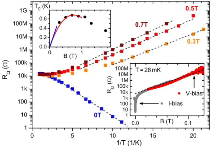
Shown in Fig.2are logRwvs. 1/Tplots for the represen- tative magnetic fields. At zero magnetic field, the sample is superconducting with the resistance exhibiting the Arrhenius- like behaviour, Rw/expðTJ0=TÞ, over three orders of the magnitude. The dashed line presents the fit yielding TJ0¼0:92 K. Such a behaviour suggests that the dissipation mechanism is thermally activated phase slips. Employing the
Ambegaokar-Halperin description of the phase diffusion through an overdamped Josephson junction,38we identify the activation energy askBTJ0¼2EJ0¼hIc0=e, whereEJ0is the Josephson coupling energy and Ic0 is the zero-temperature Josephson critical current and find Ic0’19 nA. This value
FIG. 1. High-resolution TEM images of the plan view (a) and the cross section (b) of the initial as-grown TiN film. (c) The SEM image of the sample. The black areas are the TiN film itself and the light grey areas are the etched parts.
The numbers mark contact pads. The distance between the probes 2 and 5 is 450lm and the sample width is 50lm.
It corresponds to nine squares at four- probe measurements, where the current flows between 1 and 6 contact pads. The area (accounting for a geometry factor) in two-probe measurements corresponds to 24 squares. (d) The resistance per square vs. temperature at zero magnetic field for the initial as-grown TiN film (solid line) and for the oxidized film at B¼0 T and B¼0.5 T, shown by sym- bols. (e) The representative dual current- voltage characteristics of the oxidized film atB¼0 T and B¼0.5 T atT¼50, 150, and 350 mK, the voltage axis show- ing voltages per square.
FIG. 2.Rw vs. 1/TatB¼0, 0.3, 0.5, and 0.7 T (symbols). Dashed lines show fits to the Arrhenius law. The bottom-right corner inset: matching of RwðBÞ measured at T¼28 mK for the voltage and current bias setups, respectively. The current bias setup is realized by the four-probe ac lock-in technique, with the ac current of 40 pA and the frequencyf¼1.74 Hz. In the two-probe voltage bias measurements, the ac voltage 4lV and the same fre- quency were used. The dashed line corresponds toRwðBÞ ¼R0expðB=BÞ, withB¼14 mT andR0¼6:45 kX. The top-left corner inset: the activation temperature,T0, as function of magnetic fieldB. The solid curve is the fit of T0ðBÞby Eq. (14) from Ref.39. The straight line is the low-field tangent to the curve with the slopeT0ðBÞ=B¼2:0 K=T.
042601-2 Baturinaet al. Appl. Phys. Lett.102, 042601 (2013)
remarkably compares with the independently measured low- temperature critical currentIc’10 nA. All the above is in accord with the expectations that SIT in a disordered film is of a percolative nature and that the electronic transport close to the transition is controlled by the phase diffusion over the saddle point critical junctions which couple superconducting clusters.37
The superconducting state in our film is fragile and is destroyed by extremely weak magnetic field perpendicular to the film: atT¼28 mK, the resistanceRwðBÞshoots up over three orders of magnitude within the tiny interval from 0 to 5 mT, see the bottom-right corner inset in Fig.2. Upon further increase of the field up to 0.1 T,RwðBÞgrows exponentially, gaining another three orders of magnitude. This exponential growth can be expressed by formulaRwðBÞ ¼R0expðB=BÞ.
We have foundB¼14 mT. The determined pre-exponential factorR0¼6:45 kXstrikingly coincides with the quantum re- sistance for Cooper pairs,h=ð2eÞ2.
The resistance at finite fields exhibits the Arrhenius tem- perature behavior,RwðTÞ /expðT0=TÞ. The magnitude and the non-monotonic magnetic field dependence of the activa- tion energyT0shown in the top-left corner inset of Fig.2are in accord with the previously reported data on TiN films.34–36 A change from the exponential decrease of the resistance at zero field to the mirror-symmetric exponential growth of the resistance with the decreasing temperature at finite fields demonstrates the duality between the superconducting and insulating behaviours of the critically disordered films not only in non-linearI-Vcurves but also in the linear response at both sides of the SIT. Applying the fitting procedure of T0ðBÞby Eq. (14) of Ref.39and taking into account the mag- netic field dependence of the Josephson coupling energy for two-dimensional Josephson junction arrays in the nearest neighbors approximation,40 we find Dcð0Þ=kB¼2:05 K;
Aloop¼0:98103lm2, and aEJ=Ec¼1. Notably, at low magnetic fields, this fit gives the slope b¼T0ðBÞ=B¼ 2:0 K=T (shown by the straight line in the top-left corner inset
of Fig.2), which, in its turn, immediately offers a quantitative expression for exponential growth of the resistance with the magnetic field in the low field region RwðT;BÞ
¼R0exp½bB=T. Indeed, earlier introduced B is equal to T=bdetermined independently from the linear approximation of T0ðBÞ, shown in the top inset of Fig. 2. This self- consistency in the description at both superconducting and insulating sides of the transition in terms of Josephson junc- tion network physics is paralleled by the mirror-symmetric current-voltage characteristics of the artificially manufactured one- and two-dimensional Josephson junction arrays.41–44It is further interesting to note the similarities between the behavior of TiN films bordering the SIT and other materials, InO,45–48Be,49Ga,50to name a few (see also Refs.51–53for a review).
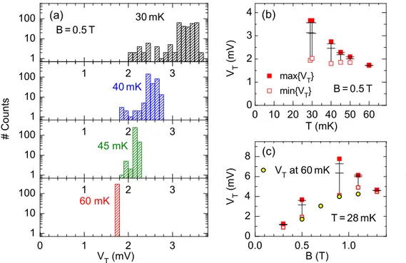
At low temperatures, theI-Vcharacteristics acquire pro- foundly switching character both in the superconducting state (at Ic) and in the magnetic-field induced insulating state, where the current exhibits a jump at some threshold switching voltage VT, see Fig. 1(e). At T <60 mK, the value of VT
becomes stochastic and varies from one measurement to another. A random distribution of the threshold voltage is det- rimental to applications.54Thus, it is important to understand the nature and borders of this behavior. To investigate the sta- tistical distribution ofVT, we have repeatedly measured many I-V characteristics for each representative temperature and external magnetic field. Figure 3displays the corresponding histograms of VT at B¼0.5 T [panel a]; panels (b) and (c) show the temperature and the magnetic field dependences of the maximal and minimal values of VT as well as indicate intervals containing 75% of the data. We observe that (i) the histograms have a sharp cut off at the maximal VT; (ii) the most probable VT is shifted towards the maximal value as temperature decreases. The above facts clearly evidence a non-Gaussian character of the VT distribution and indicate the possible glassy character of the low-temperature state.
(iii) The field-dependence of the most probable value of
FIG. 3. Histograms for theVT distribu- tion: (a)B¼0.5 T and different tempera- tures (the samplings number at each temperature is 299); (b) and (c) Temper- ature (atB¼0.5 T) and field (atT¼28 mK) dependences of the variance range of VT, maximal and minimal values shown by solid and open squares, respec- tively. Horizontal lines indicate intervals containing 75% of the data.VTvsBat T¼60 mK is shown by circles in (c).
VTðBÞ is non-monotonic and has the values close to those observed on samples which are insulating atB¼0.34(iv) At T<45 mK, the ratio of max{VTðBÞ}/min{VTðBÞ} 2 in magnetic fields below the field where the maximum ofVTðBÞ is achieved, then it drops rapidly upon further field increase.
(v) As the temperature grows, the ratio max{VT}/min{VT} reduces to unity and the random scattering ofVT vanishes.
Then at T 60 mK, the I-V characteristics become stable and fully reproducible, withVT depending on the magnetic field. Stable and extremely sharp switchingI-Vcharacteristics atTⲏ60 mK imply that in this temperature range, an ultra- thin TiN film can be used as a supersensitive sensor or a threshold detector.
To summarize, our findings break the ground for appeal- ing applications of TiN in electronics. The specific property of our films is their ability to be in either of insulating, metal- lic, or superconducting states depending on their degree of oxidation and thickness. This enables the design of a whole circuit including all the above elements but cut out of the very same film, in particular, realizing the quantum circuits with the complementary architectures analogous to the con- ventional CMOS architectures in current electronics.
Because of the sharpness of the threshold behaviour and the size of the current jump constituting several orders of magni- tude, TiN films in the vicinity of superconductor-insulator transition hold high potential for becoming a base for sensors and detectors of unprecedented sensitivity and high useful signal-to-noise ratio. The dual character of threshold diode- like switchingI-Vcharacteristics opens routes for TiN films- based logical units which can be switched between two practically non-dissipative states by the magnetic field. Crit- ically disordered TiN films constitute a single versatile plat- form for devices with dual operating characteristics and can be assembled to threshold detectors for either current or volt- age transients. Another important application is photon detection, based on the photon-induced switching between insulating, resistive, and superconducting states.
The work was supported by the Deutsche Forschungs- gemeinschaft under Grant No. 444USA113/3 and within the GRK 638, the Program “Quantum Mesoscopic and Disor- dered Systems” of the Russian Academy of Sciences, the Rus- sian Foundation for Basic Research (Grant No. 12-02-00152), and the U.S. Department of Energy Office of Science under the Contract No. DE-AC02-06CH11357.
1M. Wittmer,Appl. Phys. Lett.36, 456 (1980).
2W. Sinke, G. P. A. Frijlink, and F. W. Saris,Appl. Phys. Lett.47, 471 (1985).
3S. N. Yoganand, M. S. Raghuveer, K. Jagannadham, L. Wu, A. Karoui, and G. Rozgonyi,Appl. Phys. Lett.80, 79 (2002).
4C. A. Dimitriadis, S. Logothetidis, and I. Alexandrou, Appl. Phys. Lett.
66, 502 (1995).
5J. R. Waldrop,Appl. Phys. Lett.43, 87 (1983).
6J. Ding, Z. Liliental-Weber, E. R. Weber, J. Washburn, R. M. Fourkas, and N. W. Cheung,Appl. Phys. Lett.52, 2160 (1988).
7N. D. Cuong, S.-G. Yoon, D.-J. Kim, and B.-D. Kang,Appl. Phys. Lett.
90, 183506 (2007).
8N. D. Cuong, S.-G. Yoon, and D.-J. Kim,Appl. Phys. Lett.91, 203502 (2007).
9M. Kiuchi and A. Chayahara,Appl. Phys. Lett.64, 1048 (1994).
10S. Choi, S.-S. Kim, M. Chang, H. Hwanga, S. Jeon, and C. Kim, Appl.
Phys. Lett.86, 123110 (2005).
11S. Maikap, P. J. Tzeng, H. Y. Lee, C. C. Wang, T. C. Tien, L. S. Lee, and M.-J. Tsai,Appl. Phys. Lett.91, 043114 (2007).
12J. Narayan, P. Tiwari, X. Chen, J. Singh, R. Chowdhury, and T. Zheleva, Appl. Phys. Lett.61, 1290 (1992).
13B. W. Karr, I. Petrov, D. G. Cahill, and J. E. Greene,Appl. Phys. Lett.70, 1703 (1997).
14M. Boumerzoug, Z. Pang, M. Boudreau, P. Mascher, and J. G. Simmons, Appl. Phys. Lett.66, 302 (1995).
15A. Weber, R. Poeckelmann, and C. P. Klages,Appl. Phys. Lett.67, 2934 (1995).
16D.-H. Kim, S.-L. Cho, K.-B. Kim, J. J. Kim, J. Won Park, and J. J. Kim, Appl. Phys. Lett.69, 4182 (1996).
17M. Zeitler, J. W. Gerlach, T. Kraus, and B. Rauschenbach, Appl. Phys.
Lett.70, 1254 (1997).
18Y. Fu, Y. T. Moon, F. Yun,U.€ Ozg€€ ur, J. Q. Xie, S. Dogan, H. Morkoc, C. K. Inoki, T. S. Kuan, L. Zhou, and D. J. Smith,Appl. Phys. Lett.86, 043108 (2005).
19F. Fillot, S. Ma^ıtrejean, I. Matko, and B. Chenevier,Appl. Phys. Lett.92, 023503 (2008).
20L. Wu, H. Y. Yu, X. Li, K. L. Pey, J. S. Pan, J. W. Chai, Y. S. Chiu, C. T.
Lin, J. H. Xu, H. J. Wann, X. F. Yu, D. Y. Lee, K. Y. Hsu, and H. J. Tao, Appl. Phys. Lett.96, 113510 (2010).
21H. G. Leduc, B. Bumble, P. K. Day, B. Ho Eom, J. Gao, S. Golwala, B. A.
Mazin, S. McHugh, A. Merrill, D. C. Moore, O. Noroozian, A. D. Turner, and J. Zmuidzinas,Appl. Phys. Lett.97, 102509 (2010).
22M. R. Vissers, J. Gao, D. S. Wisbey, D. A. Hite, C. C. Tsuei, A. D.
Corcoles, M. Steffen, and D. P. Pappas, Appl. Phys. Lett.97, 232509 (2010).
23L. E. Toth, C. P. Wang, and C. M. Yen,Acta. Metall.14, 1403 (1966).
24W. Spengler, R. Kaiser, A. N. Christensen, and G. M€uller-Vogt,Phys.
Rev. B17, 1095 (1978).
25T. P. Thorpe, S. B. Qadri, S. A. Wolf, and J. H. Claassen,Appl. Phys. Lett.
49, 1239 (1986).
26W. Tsai, M. Delfino, J. A. Fair, and D. Hodul,J. Appl. Phys.73, 4462 (1993).
27Y. Seguchi, T. Tsuboi, T. Kawahara, and T. Suzuki,J. Phys. Soc. Jpn.64, 4544 (1995).
28T. Suzuki, Y. Seguchi, and T. Tsuboi,J. Phys. Soc. Jpn.69, 1462 (2000).
29T. I. Baturina, D. R. Islamov, J. Bentner, C. Strunk, M. R. Baklanov, and A. Satta,JETP Lett.79, 337 (2004).
30N. Hadacek, M. Sanquer, and J.-C. Villegier,Phys. Rev. B 69, 024505 (2004).
31B. Sacepe, C. Chapelier, T. I. Baturina, V. M. Vinokur, M. R. Baklanov, and M. Sanquer,Phys. Rev. Lett.101, 157006 (2008); Nat. Commun.1, 140 (2010).
32F. Pfuner, L. Degiorgi, T. I. Baturina, V. M. Vinokur, and M. R. Baklanov, New J. Phys.11, 113017 (2009).
33T. I. Baturina, S. V. Postolova, A. Yu. Mironov, A. Glatz, M. R. Baklanov, and V. M. Vinokur,EPL97, 17012 (2012).
34T. I. Baturina, A. Yu. Mironov, V. M. Vinokur, M. R. Baklanov, and C. Strunk,Phys. Rev. Lett.99, 257003 (2007).
35T. I. Baturina, A. Bilusic´, A. Yu. Mironov, V. M. Vinokur, M. R. Bakla- nov, and C. Strunk,Physica C468, 316 (2008).
36T. I. Baturina, A. Yu. Mironov, V. M. Vinokur, M. R. Baklanov, and C. Strunk,JETP Lett.88, 752 (2008).
37E. Shimshoni, A. Auerbach, and A. Kapitulnik,Phys. Rev. Lett.80, 3352 (1998).
38V. Ambegaokar and B. I. Halperin,Phys. Rev. Lett.22, 1364 (1969).
39M. V. Fistul, V. M. Vinokur, and T. I. Baturina,Phys. Rev. Lett. 100, 086805 (2008).
40M. Tinkham, D. W. Abraham, and C. J. Lobb, Phys. Rev. B28, 6578 (1983).
41L. J. Geerligs, M. Peters, L. E. M. de Groot, A. Verbruggen, and J. E.
Mooij,Phys. Rev. Lett.63, 326 (1989).
42P. Delsing, C. D. Chen, D. B. Haviland, Y. Harada, and T. Claeson,Phys.
Rev. B50, 3959 (1994).
43H. S. J. van der Zant, W. J. Elion, L. J. Geerligs, and J. E. Mooij,Phys.
Rev. B54, 10081 (1996).
44E. Chow, P. Delsing, and D. B. Haviland,Phys. Rev. Lett.81, 204 (1998).
45G. Sambandamurthy, L. W. Engel, A. Johansson, and D. Shahar,Phys.
Rev. Lett.92, 107005 (2004).
46G. Sambandamurthy, L. W. Engel, A. Johansson, E. Peled, and D. Shahar, Phys. Rev. Lett.94, 017003 (2005).
042601-4 Baturinaet al. Appl. Phys. Lett.102, 042601 (2013)
47M. Ovadia, B. Sacepe, and D. Shahar, Phys. Rev. Lett.102, 176802 (2009).
48O. Cohen, M. Ovadia, and D. Shahar, Phys. Rev. B 84, 100507(R) (2011).
49E. Bielejec, J. Ruan, and W. Wu, Phys. Rev. B 63, 100502(R) (2001).
50C. Christiansen, L. M. Hernandez, and A. M. Goldman,Phys. Rev. Lett.
88, 037004 (2002).
51R. S. Newrock, C. J. Lobb, U. Geigenm€uller, and M. Octavio, “The two- dimensional physics of Josephson junction arrays,”Solid State Phys.54, 263 (1999).
52V. F. Gantmakher and V. T. Dolgopolov,Phys. Usp.53, 1 (2010).
53T. I. Baturina and V. M. Vinokur, “Superinsulator–superconductor duality in two dimensions,”Ann. Phys.(published online); preprintarXiv:1209.0530.
54D. M. Kaplan, V. A. Sverdlov, and K. K. Likharev, Phys. Rev. B68, 045321 (2003).