Ge(100) surfaces in CVD ambient
D i s s e r t a t i o n
zur Erlangung des akademischen Grades d o c t o r r e r u m n a t u r a l i u m
(Dr. rer. nat.) im Fach Physik
eingereicht an der
Mathematisch-Naturwissenschaftlichen Fakultät I der Humboldt-Universität zu Berlin
von
Dipl.-Ing. Sebastian Brückner
Präsident der Humboldt-Universität zu Berlin:
Prof. Dr. Jan-Hendrik Olbertz
Dekan der Mathematisch-Naturwissenschaftlichen Fakultät I:
Prof. Stefan Hecht, PhD
Gutachter/innen: 1. Prof. Dr. Recardo Manzke 2. Prof. Dr. Thomas Hannappel 3. Prof. Dr. Wolf Gero Schmidt Tag der mündlichen Prüfung: 21.11.2013
In dieser Arbeit wurde die atomare Oberflächenstruktur von Si(100)- und Ge(100)-Oberflächen untersucht, die mittels metallorganischer chemischer Gasphasenabscheidung (MOCVD) für anschließende Heteroepitaxie von III-V-Halbleitern präpariert wurden. An der Grenzfläche des Gruppe-IV-Substrates zur III-V-Schicht führen atomare Einfachstufen auf der Substratoberfläche zu Antiphasenunordnung in der epitaktisch gewachsenen Schicht. Dies kann jedoch durch Erzeugung von atomaren Doppelstufen auf dem Substrat vermieden werden. Die MOCVD- Prozessgasumgebung hat einen starken Einfluss auf die Domänen- und Stufenbildung der Si(100)- und Ge(100)-Oberfläche. Deswegen wurden in situ Reflexions-Anisotropie-Spektroskopie (RAS) und verschiedene Ultrahochvakuum-(UHV)-basierte oberflächensensitive Messmethoden verwendet, um die verschiedenen Oberflächen in Abhängigkeit von der Präparation zu charakterisieren. In situ RAS ermöglicht die Identifizierung der Oberflächenstruktur sowie Zuordnung der entscheidenden Prozessschritte und somit auch Kontrolle über die Oberflächenpräparation, insbesondere der Domänenbildung auf Si(100)- und Ge(100)- Oberflächen. Sowohl Si(100) als auch Ge(100) zeigen eine starke Wechselwirkung mit dem Prozessgas H2,die letztlich zur Bildung einer Monohydrid-Bedeckung der Oberflächen während der Präparation führt. Detaillierte Analyse verschiedener Si(100)-Oberflächen und Einflüsse der Hauptprozessparameter weisen auf Si-Abtrag während der Präparation unter hohem H2-Druck hin. Die Erzeugung von Leerstellen auf den Terrassen bewirkt eine kinetisch bedingte Oberflächenstruktur, basierend auf Diffusion von Si-Leerstellen und Atomen. Entsprechend unserer in situ RAS- und Rastertunnelmikroskopie-(STM)-Messungen führt dies auf verkippten Si(100)-Substraten zur Bildung von ungewöhnlichen DA-Doppelstufen, bei denen die Dimere auf den Terrassen senkrecht zur Stufenkante orientiert sind, während auf exakten Si(100)-Substraten ein schichtweiser Abtragsprozess stattfindet. Präparation unter niedrigem H2-Druck hingegen führt zu einer Domänen- und Stufenstruktur, die energetisch bedingt ist. Im Gegensatz zur Si(100)-Oberfläche zeigen verkippte Ge(100)-Oberflächen keinen direkten Einfluss der H2- Prozessgasumgebung auf die Stufenstruktur. Bei der Ge(100)-Oberfläche ist der Einfluss von Gruppe-V-Elemente auf die Stufen- und Domänenbildung sowie auf die nachfolgende III-V- Nukleation entscheidend. In dieser Arbeit wurde der Einfluss von As- und P-Angebot auf die Ge(100)-Oberfläche untersucht. Detaillierte Untersuchungen der As-terminierten Ge(100)- Oberflächen zeigen die Ausbildung von eindomänigen Oberflächen unterschiedlicher Dimerorientierung und deutlich unterschiedlicher Stufenstruktur in Abhängigkeit von Temperatur und As-Quelle. Angebot von P an Ge(100)-Oberflächen durch Heizen in Tertiarybutylphosphin führt zu einer ungeordneten, P-terminierten Ge(100)-Oberfläche, wie Beugung niederenergetischer Elektronen (LEED) zeigt. Den in situ RAS-Messungen zu Folge ist die Ge(100):P-Oberfläche instabiler als die Ge(100):As-Oberfläche. Die nachfolgende III-V- Heteroepitaxie auf Gruppe-IV(100)-Substraten hängt empfindlich von der Domänenausbildung der Si(100) und Ge(100)-Oberflächen ab. Hier wurde RAS als in situ Messmethode zur Kontrolle aller Prozessschritte während der Präparation von Si(100) und Ge(100) in MOCVD-Umgebung etabliert.
In the present work, the atomic surface structure of Si(100) and Ge(100) surfaces prepared in metalorganic chemical vapor phase deposition (MOCVD) ambient was studied with regard to subsequent heteroepitaxy of III-V semiconductors on group IV(100) substrates. At the crucial interface between the group-IV substrate and the III-V layer, single-layer steps on the substrate surface induce anti-phase disorder in the epitaxial film. In principle, double-layer stepped substrates can be employed to avoid anti-phase disorder. The MOCVD process gas environment strongly influences the domain and step formation of Si(100) and Ge(100) surfaces. To this end, in situ reflection anisotropy spectroscopy (RAS) and several other ultra-high vacuum-based (UHV) surface sensitive methods were applied to investigate the different surfaces dependent on the preparation. In situ RAS enabled identification of the surface structure and correlation of the crucial process steps, leading to complete control of surface preparation, in particular the domain formation of Si(100) and Ge(100) surfaces. Both the Si(100) and Ge(100) surface strongly interact with H2 process gas which eventually leads to monohydride termination of the surfaces during preparation. Detailed analysis of Si(100) surfaces and the influence of the main process parameters indicated Si removal during processing in high H2 pressure ambient. The generation of vacancies on the terraces induces a kinetically driven surface structure based on diffusion of vacancies and Si atoms leading to energetically unexpected step structures. Consequently, anomalous DA-type double-layer steps, with dimers on the terraces oriented perpendicular to the step edges, are formed on vicinal Si(100) substrates according to in situ RAS and scanning tunneling microscopy (STM) measurements, whereas Si layer-by-layer removal occurs on large terraced substrates. However, processing in low H2 pressure ambient leads to a step and domain structure which is energetically driven. In contrast to Si(100), H2 annealed vicinal Ge(100) surfaces indicate no direct influence of the H2 process gas ambient on the step structure. At the Ge(100) surface, group-V elements strongly influence step and domain formation as well as subsequent III-V nucleation. In this work, the exposure of vicinal Ge(100) substrates to As and P was studied. Detailed characterization of Ge(100):As surfaces showed the formation of single domain surfaces with different majority domain and significantly different step structures depending on temperature and As source, respectively. In contrast, exposure to P by annealing in tertiarybutylphosphine leads to a very disordered P-terminated vicinal Ge(100) surface according to low energy electron diffraction (LEED) measurements. In situ RAS measurements showed that the Ge(100):P surface is less stable compared to the Ge(100):As surfaces. The subsequent III-V heteroepitaxy strongly depends on the step and the domain structure of the group-IV(100) substrate. Here, RAS was established as a powerful in situ method to control all process steps of Si(100) and Ge(100) surface preparation in MOCVD ambient.
Zusammenfassung... III Abstract ... V Publications ... XI
1. Introduction ... 1
2. Theoretical and experimental background ... 5
2.1 Multi-junction solar cells ... 5
2.2 III-V-on-IV(100) heteroepitaxy ... 8
2.2.1 Anti-phase domains ... 9
2.3 Si(100) and Ge(100) surfaces... 12
2.3.1 Surface properties ... 12
2.3.2 Hydrogen on Si(100) and Ge(100) ... 14
2.3.3 Vicinal surfaces ... 17
2.3.4 Step formation ... 18
2.3.4.1 Influence of hydrogen ... 19
2.3.4.2 Si removal and growth processes ... 20
2.3.4.3 Influence of group-V elements ... 21
2.4 Experimental background ... 24
2.4.1 Metalorganic chemical vapor deposition ... 24
2.4.1.1 MOCVD-to-UHV transfer system... 26
2.4.2 Reflection anisotropy spectroscopy ... 27
2.4.3 X-ray photoelectron spectroscopy ... 31
2.4.4 Low energy electron diffraction ... 34
2.4.5 Scanning tunneling microscopy ... 37
2.4.6 Fourier-transform infrared spectroscopy ... 38
2.4.7 Sample preparation and standard MOCVD processes ... 38
2.4.7.1 Standard Si(100) process ... 38
2.4.7.2 Standard Ge(100) process ... 40
2.5 State of the art: Si(100) surfaces in hydrogen ambient ... 41
2.5.1 Oxide removal and clean surface ... 41
2.5.2 Step and domain structure after deoxidation ... 44
2.5.3 Hydrogen termination of MOCVD prepared Si(100) ... 46
2.5.3.1 Direct proof of monohydride termination ... 46
3. Surface studies of MOCVD-prepared Si(100) and Ge(100) surfaces ... 53
3.1 Silicon (100) surfaces ... 53
3.1.1 Interaction of Si(100) with H2 process gas ... 53
3.1.1.1 In situ RA spectra during preparation of vicinal Si(100) ... 54
3.1.1.2 In situ observation of hydrogen adsorption during cooling .... 56
3.1.1.3 In situ RAS observation of H desorption... 58
3.1.2 Anomalous double-layer step formation ... 59
3.1.2.1 Preparation of Si(100) with majority A-type domain ... 60
3.1.2.2 Direct observation of DA steps on Si(100) 2° ... 62
3.1.2.3 In situ observation of domain formation ... 63
3.1.2.4 DA step formation process ... 65
3.1.3 Domain-sensitive in situ observation of layer-by-layer removal 66 3.1.3.1 In situ observation of layer-by-layer removal ... 67
3.1.3.2 Vacancy formation and layer-by-layer removal mechanism .. 69
3.1.3.3 Etch process on Si(100) in H2 ambient ... 72
3.1.3.4 Influence of preparation route on domain formation ... 73
3.1.4 In situ control of dimer orientation on Si(100) ... 73
3.1.4.1 Domain formation in dependence of H2 pressure ... 74
3.1.4.2 In situ observation of domain formation at low H2 pressure .. 76
3.1.4.3 Domain formation on high offcut substrates ... 78
3.2 Germanium (100) surfaces ... 82
3.2.1 Ge(100) surface preparation in H2 ambient ... 82
3.2.1.1 Oxide removal and preparation of clean Ge(100) ... 83
3.2.1.2 Direct evidence for monohydride termination on Ge(100) .... 85
3.2.1.3 RA spectrum of vicinal Ge(100):H ... 85
3.2.2 Interaction of Ge(100) with H2 process gas ... 87
3.2.2.1 RA spectra of clean and monohydride terminated Ge(100) ... 88
3.2.2.2 H2 desorption kinetics at Ge(100) ... 90
3.2.2.3 H termination of Ge(100) during processing ... 94
3.2.3 In situ control of As dimer orientation on Ge(100) surfaces ... 96
3.2.3.1 RA spectra of vicinal Ge(100):As ... 97
3.2.3.2 Benchmarking of Ge(100):As RA spectra ... 99 3.2.3.3 As dimer orientation in dependence on process parameters . 103
3.2.4.2 Chemical composition and surface reconstruction ... 109
3.2.4.3 In situ observation of P desorption from Ge(100) ... 112
3.3 Key aspects of Si(100) and Ge(100) surface preparation ... 114
4. Conclusion ... 119
Bibliography ... 123
Danksagung ... 143
Major publications:
1. S. Brückner, H. Döscher, P. Kleinschmidt, and T. Hannappel, “In situ investigation of hydrogen interacting with Si(100)”, Applied Physics Letters, vol. 98, no. 21, p.
211909, 2011.
2. S. Brückner, H. Döscher, P. Kleinschmidt, O. Supplie, A. Dobrich, and T.
Hannappel, “Anomalous double-layer step formation on Si(100) in hydrogen process ambient”, Physical Review B, vol. 86, no. 19, p. 195310, 2012.
3. S. Brückner, P. Kleinschmidt, O. Supplie, H. Döscher, and T. Hannappel,
“Domain-sensitive in situ observation of layer-by-layer removal at Si(100) in H2
ambient”, New Journal of Physics, vol. 15, no. 11, p. 113049, 2013.
4. S. Brückner, E. Barrigón, O. Supplie, P. Kleinschmidt, A. Dobrich, C. Löbbel, I.
Rey-Stolle, H. Döscher, and T. Hannappel, “Ge(100) surfaces prepared in vapor phase epitaxy process ambient”, physica status solidi (RRL) – Rapid Research Letters, vol. 6, no. 4, pp. 178–180, 2012.
5. S. Brückner, O. Supplie, E. Barrigón, J. Luczak, P. Kleinschmidt, I. Rey-Stolle, H.
Döscher, and T. Hannappel, “In situ control of As dimer orientation on Ge(100) surfaces”, Applied Physics Letters, vol. 101, no. 12, pp. 121602–121602–4, 2012.
6. E. Barrigón, S. Brückner, O. Supplie, P. Kleinschmidt, I. Rey-Stolle, and T.
Hannappel, “Optical in situ monitoring of hydrogen desorption from Ge(100) surfaces”, Applied Physics Letters, vol. 102, no. 11, pp. 111608–111608–4, 2013.
7. E. Barrigón, S. Brückner, O. Supplie, H. Döscher, I. Rey-Stolle, and T. Hannappel,
“In situ study of Ge(100) surfaces with tertiarybutylphosphine supply in vapor phase epitaxy ambient”, Journal of Crystal Growth, vol. 370, pp. 173–176, 2013.
8. O. Supplie, S. Brückner, O. Romanyuk, H. Döscher, P. Kleinschmidt, F. Grosse, and T. Hannappel, “Atomic scale analysis of the GaP/Si(100) heterointerface by in situ reflection anisotropy spectroscopy and ab initio density functional theory”, submitted, 2013.
9. H. Döscher, A. Dobrich, S. Brückner, P. Kleinschmidt, and T. Hannappel, “Si(100) surfaces in a hydrogen-based process ambient”, Applied Physics Letters, vol. 97, no. 15, 2010.
15, 2011.
11. H. Döscher, S. Brückner, and T. Hannappel, “Investigation of oxide removal from Si(100) substrates in dependence of the MOVPE process gas ambient”, Journal of Crystal Growth, vol. 318, no. 1, pp. 563–569, 2011.
12. S. Brückner, H. Döscher, T. Hannappel, P. Kleinschmidt, O. Supplie, and A.
Dobrich, “Verfahren zur Oberflächenpräparation von Si(100)-Substraten”, Deutsche Patentanmeldung 102011122749.4, 2013.
Other publications:
13. H. Döscher, O. Supplie, S. Brückner, T. Hannappel, A. Beyer, J. Ohlmann, and K.
Volz, “Indirect in situ characterization of Si(100) substrates at the initial stage of III-V heteroepitaxy”, Journal of Crystal Growth, vol. 315, no. 1, pp. 16–21, 2011.
14. S. Brückner, O. Supplie, E. Barrigon, P. Kleinschmidt, A. Dobrich, I. Rey-Stolle, C. Algora, H. Döscher, and T. Hannappel, “Si(100) versus Ge(100): Watching the interface formation for the growth of III-V-based solar cells on abundant substrates”, 37th IEEE Photovoltaic Specialists Conference (PVSC), pp. 002538–
002542, 2011.
15. S. Brückner, O. Supplie, E. Barrigón, A. Dobrich, J. Luczak, C. Löbbel, I. Rey- Stolle, P. Kleinschmidt, H. Döscher, and T. Hannappel, “In situ control of Si(100) and Ge(100) surface preparation for the heteroepitaxy of III-V solar cell architectures”, AIP Conference Proceedings, vol. 1477, no. 1, pp. 32–35, 2012.
16. P. Kleinschmidt, H. Döscher, O. Supplie, A. Dobrich, S. Brückner, and T.
Hannappel, “MOVPE Preparation of Double-Layer Stepped Silicon(100) for III- V-on-Silicon Solar Cells”, 27th European Photovoltaic Solar Energy Conference and Exhibition, Frankfurt, pp. 67 – 69, 2012.
17. T. Roesener, H. Döscher, A. Beyer, S. Brückner, V. Klinger, A. Wekkeli, P.
Kleinschmidt, C. Jurecka, J. Ohlmann, K. Volz, W. Stolz, T. Hannappel, A. W.
Bett, and F. Dimroth, “MOVPE Growth of III-V Solar Cells on Silicon in 300MM Closed Coupled Showerhead Reactor,” 25th European Photovoltaic Solar Energy Conference and Exhibition / 5th World Conference on Photovoltaic Energy Conversion, Valencia, Spain, pp. 964 – 968, 2010.
Hannappel, “VPE preparation of Si(100) and in situ characterization via RAS”, oral presentation, 24. DGKK Workshop Epitaxie von III/V Halbleitern, Berlin, 2009.
2. S. Brückner, H. Döscher, A. Dobrich, O. Supplie, P. Kleinschmidt and T. Hannappel,
“In situ characterization of hydrogen termination of VPE prepared Si(100) via RAS”, 24. DGKK Workshop Epitaxie von III/V Halbleitern, Aachen, 2010.
3. S. Brückner, H. Döscher, A. Dobrich, O. Supplie, P. Kleinschmidt, T. Hannappel,
“Preparation and in situ control of Si(100) substrates for III-V on Si via MOVPE”, oral presentation, Compound Semiconductor Week 2011 / 23rd International Conference on Indium Phosphide and Related Materials, Berlin, 2011.
4. S. Brückner, E. Barrigón, O. Supplie, J. Luczak, C. Löbbel, P. Kleinschmidt, H.
Döscher, T. Hannappel, "In situ spectroscopy and surface characterization of MOVPE-prepared Ge(100) for III-V heteroepitaxy" poster presentation, 13th International Conference on the Formation of Semiconductor Surfaces and Interfaces, Prag, Czech Republic, 2011.
5. S. Brückner, E. Barrigón, O. Supplie, J. Luczak, C. Löbbels, P. Kleinschmidt, H.
Döscher, T. Hannappel, “Atomic surface structure of Ge(100) surfaces in vapor phase epitaxy ambient”, poster presentation, 28th European Conference on Surface Science, Wroclaw, Poland, 2011.
6. S. Brückner, O. Supplie, E. Barrigón, A. Dobrich, J. Luczak, C. Löbbel, I. Rey-Stolle, P. Kleinschmidt, H. Döscher, and T. Hannappel, “In situ control of Si(100) and Ge(100) surface preparation for the heteroepitaxy of III-V solar cell architectures“,oral presentation, 8th International Conference on Concentrating Photovoltaic Systems, Toledo, Spain, 2012.
7. S. Brückner, O. Supplie, E. Barrigón, J. Luczak, P. Kleinschmidt , H. Döscher, and T.
Hannappel, „In situ control of dimer orientation on Si(100) and Ge(100) surfaces“, oral presentation, 27. DGKK Workshop Epitaxie von III/V Halbleitern, Erlangen 2012.
8. S. Brückner, E. Barrigón, O. Supplie1, A. Dobrich, J. Luczak, C. Löbbel, I. Rey- Stolle, P. Kleinschmidt, H. Döscher and T. Hannappel, “In situ control of the Ge(100) surface domain structure for III-V multi-junction solar cells”, oral presentation, 9.
International Conference on Concentrating Photovoltaic Systems, Miyazaki, Japan 2013.
The worldwide power consumption of mankind is increasing every year due to rising population and living standard [1]. Currently, fossil fuels present the main power sources.
Beside limited resources and soon depletion of oil and gas, their consumption is correlated with increasing environmental damage due to exploitation and CO2 emission.
Rising cost and possible power shortages as well as better environmental sustainability demand fast development of renewable energy sources.
While photovoltaic (PV) has the potential of providing a substantial share of electricity worldwide, to date its contributions to electricity generation is still very small due to relatively high energy production costs or low conversion efficiencies of solar cells. In 2012, only 5 % of the net electricity generation was supplied by solar cells in Germany [2]. The theoretical efficiency η of a single-band gap solar cell is set by the Shockley- Queisser limit to be about 30 % [3]. The Shockley-Queisser limit of a single-band gap solar cell can be exceeded by stacking solar cells with different band gaps on top of each other in so-called multi-junction solar cells [4]. III-V semiconductors are ideally suited for monolithic growth of multi-junction solar cells due to their superior optoelectronic properties and tunability of band gaps and lattice constant in a wide range by choice of composition. MOCVD is the established preparation technique for large-scale and high- quality III-V semiconductor growth [5]. Current industry standard is a GaInP/GaAs/Ge(100) triple junction solar cell which achieves device efficiencies over 40% [6].
Higher cell efficiency as well as cheaper production costs drive intensive research for the heteroepitaxial integration of III-V based multi-junction solar cells on Si(100) substrates.
Compared to conventional III-V or Ge substrates, silicon exhibits much lower substrate costs and better availability. Si(100) substrates combine very attractive material properties and benefit from extensive research and technological experience, due to their scientific and technological relevance. Integration of III-V semiconductors and Si microelectronics might also enable new high-performance devices [7,8], stimulating intense research activities in this field since the 1980s [9].
Very low defect densities are required for high quality devices in the subsequently grown III-V films. However, the transition from Si(100) to III-V semiconductors presents a difficult challenge due to lattice mismatch, different thermal expansion coefficients, and problems of polar-on-non-polar heteroepitaxy [10]. For the latter, the interface and surface formation plays a crucial role during III-V-on-IV(100) heteroepitaxy [9]:
Formation of single-domain substrate surfaces with double-layer steps is essential to avoid so-called APDs, which arise depending on the step structure of the (100) substrate surface and are associated with planar defects in the III-V material.
With a view to III-V-on-silicon epitaxy, we use a MOCVD system with H2 as process gas at a range from a few millibars to atmospheric pressure. However, most knowledge about Si(100) surfaces has been obtained from studies based on preparation in ultra-high vacuum (UHV), where standard surface science methods can easily be applied. Si(100) preparation in H2 ambient differs considerably [11–14] from well established UHV preparation [15–19]. On the other hand, Ge(100) is the standard substrate for multi- junction solar cells, but little is known about surface preparation and formation of the crucial heterointerface in MOCVD ambient. Processes in MOCVD ambient are very complex due to competition between energetic and kinetic processes, interaction of process gas and sample surface, presence of precursors, as well as III-V residuals in the reactor from previous runs. Since the process gas ambient limits access to UHV-based surface science techniques, in situ characterization of the sample surfaces is required to understand surface preparation in MOCVD ambient. Reflection anisotropy spectroscopy (RAS) is ideally suited for in situ monitoring of sample surfaces during MOCVD processing [20,21]. However, the origin of RAS signatures is very complex and requires careful analysis for identification [22–24,24–26].
The goal of this work is to study the influences of the MOCVD process parameters on the atomic surface structure of Si(100) and Ge(100) substrates, enabling the preparation of single-domain surfaces for subsequent III-V heteroepitaxy. In particular, the influence of the main process parameters such as temperature, type of process gas and pressure, and precursors on the step and domain formation was analyzed. Correlation of in situ RA
signals of Si(100) and Ge(100) surfaces for in situ surface characterization during MOCVD preparation. RAS signals of Si(100) surfaces are already relatively well understood due to numerous experimental and theoretical studies [24,25,27–35].
However, in the case of Ge(100) only scarce reports in literature exist [36,37].
Applying in situ RAS and UHV-based surface sensitive methods, we investigated the removal of oxides and other contamination from the substrates, the interaction between process gas and substrate surface, the influence of H2 ambient on the step and domain formation, and the influence of As and P exposure on the surface structure of Ge(100). In situ RAS enabled control of domain formation by adjustment of the relevant process parameters.
In this section, the theoretical background of multi-junction solar cells, III-V-on-IV(100), and the Si(100) and Ge(100) surfaces is discussed. Further, the experimental methods of this work and the basic MOCVD processes are presented. As a starting point for this work, state-of-the-art Si(100) preparation in MOCVD ambient and RAS results of Si(100) and Ge(100) surfaces are summarized.
2.1 Multi-junction solar cells
Solar cells enable direct conversion of sunlight into electrical energy. They consist of semiconductor material with a specific band gap Eg and a p-n-junction. Only the photons with energy larger than the band gap are absorbed leading to generation of electron-hole pairs. The electron-hole pairs are separated by the electric field at the p-n-junction resulting in a photoelectric voltage between front- and back-contact of the solar cell.
Principally, the conversion efficiency η of the incoming radiation into electrical energy depends on the band gap of the solar cell material: Photons with energy ħω < Eg cannot be absorbed and will be transmitted through the material (transmission losses). Only the photons with ħω = Eg are ideally converted, since the photon energy larger than the band gap ΔE = ħω - Eg is converted into heat via phonon interactions in the crystal lattice within few picoseconds (thermalization losses). Accordingly, Shockley and Queisser calculated the conversion efficiency η of a single-junction solar cell without concentration to be limited at about 30 % [3].
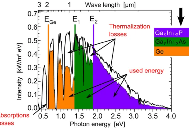
Multi-junction solar cells consist of a combination of solar cells with different band gaps in serial connection which enables efficiencies beyond the Shockley-Queisser limit by reduction of thermalization and transmission losses. Fig. 1 illustrates the better exploitation of the solar spectrum by a GaInP/GaInP/Ge triple junction solar cell.
Fig. 1: Standard solar spectrum ASTM G-173-03 for terrestrial irradiance at an effective air mass of 1.5 atmospheres and its electrical yield by a triple junction solar cell based on the combination of GaInP/GaInP/Ge (colored areas) considering absorption and thermalization losses. The colored lines refer to the band gaps of the different materials indicating their absorption edges (after [38]).
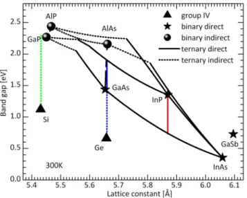
While early III-V tandem cells consisted of GaInP top cells grown on GaAs bottom cells [4], state-of-the-art triple junction solar cells are fabricated on Ge(100) substrates which serve as a low band gap bottom cell below a GaInP/GaAs tandem cell. Low defect densities in the epitaxially grown films as well as ideal band gap combinations are crucial for high performance solar cell devices. Hence, III-V semiconductors exhibit ideal properties for realization of multi-junction solar cells, since ternary or higher order compounds enable band gap tuning as well as lattice matching over a wide range. The plot of band gap over lattice constant of III-V semiconductors and elemental semiconductor (Fig. 2) clearly shows the potentials of III-Vs and challenges of the heteroepitaxy on group IV substrates.
Current matching of the sub-cells limits the efficiency of the whole solar cell, due to serial connection of the individual sub-cells. A further sub-cell with a band gap of 1.0 eV
is required to improve current matching in current triple-junction cells [39], which is not available on the lattice constant of Ge and GaAs. An alternative low-band gap tandem could be realized on InP(100) substrates [40], which exhibits disadvantageous high material prices and availability. Therefore, Si(100) substrates present another option as alternative substrate. However, a change of the lattice constant is required to reach the composition regime of classical III-V compounds with direct band gap.
So far, multi-junction solar cells were mainly established to power satellites in space due to their high efficiency and production costs. Currently, progress in the development of concentrator systems (concentrator photovoltaic – CPV) makes terrestrial application of multi-junction solar cells competitive to other techniques [6]. Here, lenses or mirrors focus the sunlight on a smaller solar cell area, and a tracking system follows the course of the sun. Typically, concentrations are in the range of 500 to 1000 suns.
2.2 III-V-on-IV(100) heteroepitaxy
Heteroepitaxial growth of III-V semiconductors on Si(100) and Ge(100) substrates is technologically highly desired. III-V semiconductors provide excellent material properties for high-efficiency optoelectronic devices, but suffer from high material costs. Group- IV(100) substrates present cheaper substrates for applications such as multi-junction solar cells [41,42], and lasers [8]. Furthermore, III-V/Si heteroepitaxy enables the monolithic integration of III-V optoelectronics with well established Si microelectronics.
Fig. 2: Band gap over lattice constant plot for III-V semiconductors and their compounds, as well as group IV semiconductors. Solid and dotted lines present ternary III-V compounds with direct and indirect band gap, respectively. Colored lines represent lattice matched heterostructure on Si, Ge, GaAs, and InP substrates relevant for solar cells.
The main challenges of III-V-on-IV(100) heteroepitaxy are related to the crucial differences in the material parameters and formation of the heterointerface:
• lattice mismatch: different lattice constant of substrate and film result in tensile or compressive lattice strain. Misfit dislocations form to relieve stress in the epitaxially grown films [43].
• different thermal expansion coefficient: typical growth temperatures are between 670 and 970 K; after growth, strain may occur when the layers are cooled down and contract differently, resulting in crack formation [44].
• interdiffusion at the heterointerface may induce cross-doping in the substrate or the epitaxial films, e.g. Ge outdiffusion into GaAs [45,46].
• polar-on-non-polar heteroepitaxy: the heterointerface induces problems such as charge neutrality or anti-phase domains [9].
GaP (aGaP = 5.45 Å) exhibits a small lattice mismatch to Si (aSi = 5.43 Å) of only 0.37 %.
Thin GaP films grow pseudomorphically on Si(100) substrates below the critical thickness resulting in GaP/Si(100) quasi-substrates [47]. Successive change of the lattice constant in subsequently grown III-V buffer layers by changing the ternary material composition, so-called grading, enables access to III-V compounds that are relevant for photovoltaic application. Grading layers are intended to relieve the strain and reduce the impact of defects such as misfit dislocations or threading dislocations [48–50]. On the other hand the novel material system of dilute nitrides (GaIn)(NAsPSb), which features incorporation of small amounts of N (<5%), enables lattice matched growth on Si(100) and a direct band gap [8,51–53]. In case of Ge(100), (In)GaAs and GaInP layers can be grown lattice matched.
2.2.1 Anti-phase domains
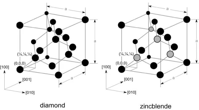
One of the most important defects to avoid during III-V/IV(100) heteroepitaxy are anti- phase domains (APDs) that originate from the polar-on-non-polar heterointerface [9]. Si and Ge crystallize in the diamond structure which equals two interpenetrating fcc sublattices (see Fig. 3). Each atom is connected to its four nearest neighbors by four tetrahedral bonds that differ in spatial orientation for the two sublattices. Both sublattices are occupied by the same type of atom species. In contrast, III-V semiconductors exhibit a zincblende structure, where the two sublattices are occupied by different atomic species.
Accordingly, the symmetry in the zincblende structure is reduced compared to the diamond structure. In a single-domain crystal, only one sublattice orientation exists.
Fig. 3: 3D sketch of the diamond and zincblende lattice structure.
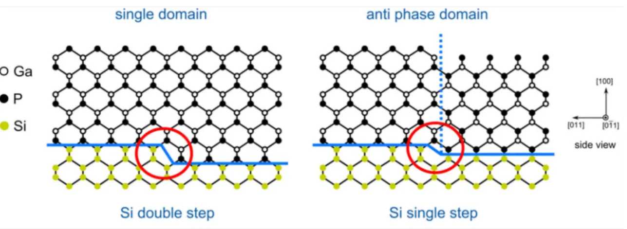
Any real Si(100) and Ge(100) surface exhibits steps. In case of single-layer steps (or an odd number height) undesired III-III or V-V bonds are formed at the step edges during III- V film growth assuming the same element as first monolayer on all terraces (Fig. 4, right side). These bonds represent electrically charged defects, so-called anti-phase boundaries (APB). APBs propagate through the III-V crystal during growth separating anti-phase domains (APDs). However, APDs can be avoided by double-layer (or even numbered) steps on the group-IV(100) substrate where the sublattice orientation in the III-V film is preserved (Fig. 4, left side).
Hence, formation of double-layer steps on the group-IV(100) substrates is a crucial prerequisite for subsequent APD-free III-V heteroepitaxy. Double-layer step formation is very well studied in UHV-based preparation ambient. However, much less is known during preparation in MOCVD where the presence of a process gas complicates access to standard surface science techniques. Step formation processes will be discussed in section 2.3.4.
Fig. 4: Schematic diagram of APD formation. At double-layer steps, the sublattice orientation remains, while single-layer steps induce anti-phase boundaries (blue dotted line).
2.3 Si(100) and Ge(100) surfaces
While the first transistor was made from germanium [54], nowadays, the silicon based microelectronic industry prevails due to the success of CMOS (complementary metal oxide semiconductor) technology. For most applications controlling the microscopic Si(100) and Ge(100) surface structure is crucial due to the influence of defects as well as of step structures. Accordingly, Si(100) belongs to the most frequently studied surfaces, due to its unequalled relevance in microelectronics. There is a renewed interest in the Ge(100) surface as substrate for III-V semiconductor solar-cells [42], as well as for applications in microelectronics [55], and nanotechnology [56]. Both Si and Ge are group IV elements and consequently exhibit four valence electrons. Both elements crystallize in the diamond structure due to sp3 hybrid orbital formation (see Fig. 3). The atoms form covalent bondings where every atom is surrounded by for nearest neighbors in a tetrahedral configuration. The lattice constants are 5.431 Å for Si and 5.658 Å for Ge.
Pure Si and Ge are intrinsic semiconductors with indirect band gaps at 1.12 eV and 0.66 eV, and direct band gaps at 3.4 eV and 0.8 eV, respectively.
The following section reports on the Si(100) and Ge(100) surface regarding surface reconstruction, hydrogen termination, as well as step and domain formation.
2.3.1 Surface properties
Regarding surface properties, the Si(100) and the Ge(100) surface exhibit a lot of similarities. Both surfaces reconstruct by forming bonds between pairs of neighboring surface atoms (dimerization). In the case of Si(100), Schlier and Fansworth [57] first discovered the (2×1) surface reconstruction by LEED measurements. In comparison to the unreconstructed surface the reconstructed surface reduces the number of dangling bonds from two to one. Hereby, two neighboring surface atoms move out of equilibrium position to bond with each other. The resulting dimers are arrayed in rows parallel to the
[011] direction (see Fig. 5). The Si dimers exhibit a bond length of 2.2-2.4 Å [58,59]
which is similar to the Si-Si distance in the bulk crystal. Dimerization induces an anisotropic surface stress tensor with compressive stress along dimer row direction and tensile stress perpendicular to the dimer rows. The stress of the crystal structure extends into the fifth layer [60].
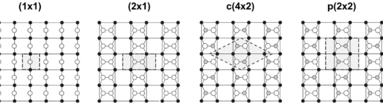
Fig. 5: Ball and stick model of the Si(100) and Ge(100) surface: (1×1) ideal unreconstructed surface, (2×1) reconstruction with symmetric dimers, c(4×2) and p(2×2) reconstruction due to dimer buckling.
Grey areas represent the unit cell of the surface reconstruction (after Zandvliet [61]).
On Si(100), the dimers are buckled by about 19° [62,63] to further reduce the surface energy (see Fig. 6). The formation of antisymmetric dimers is favored by approximately 0.14 eV per dimer compared to the symmetrical configuration, corresponding to the formation of a c(4×2) and a p(2×2) surface reconstruction, respectively (see Fig. 5). On Si(100), the dimers oscillate at room temperature resulting in the observed (2×1) reconstruction in STM. Low temperature STM evidenced the presence of buckled dimers [64–66]. In contrast, on Ge(100) dimer buckling is present at ambient temperature. Stripes of (2×1), c(4×2) and p(2×2) surface reconstructions coexist on very clean surfaces [61].
Fig. 6: Side view of two buckled dimers (after Zandvliet [61]).
The induced anisotropic surface stress tensor due to dimerization can be reduced by formation of surface reconstruction domains with mutually perpendicular dimer orientation. The domains are separated by monoatomic steps (step height a0/4 = 1.36 Å
for Si(100)), leading to a balanced distribution of (2×1) and (1×2) domains on nearly exact Si(100) surfaces [67].
2.3.2 Hydrogen on Si(100) and Ge(100)
Hydrogen termination on Si(100) leads to passivation of the reactive clean surface, reducing its susceptibility to oxidation and other contamination. The hydrogenated Si(100) surface prepared in UHV by application of atomic hydrogen exhibits three different surface reconstructions with increasing hydrogen chemical potential (see Fig. 7):
a monohydride (2×1), a mixed (3×1), and a dihydride (1×1) phase [68].
Fig. 7: Side view of the different surface reconstructions induced by adsorption of atomic hydrogen (after [69]).
In case of the monohydride phase, the number of hydrogen atoms equals the number of Si surface atoms, since H atoms saturate the remaining dangling bonds of the Si dimers. As a consequence of the saturation of the dangling bonds, interaction between them is suppressed. Hence, dimer buckling does not occur on the monohydride terminated surface leading to a (2×1) surface reconstruction. Monohydride termination occurs for hydrogen coverage θ ≤ 1 ML by exposure to moderate amounts of atomic hydrogen, but exposure at room temperature does not result in a well-ordered monohydride terminated (2×1) Si(100) surface due to possible formation of higher hydrides. Hydrogenation exceeding
saturation of the second dangling bond with hydrogen for temperatures below 570 K. A mixed (3×1) (θ = 1.5 ML) or a dihydride (1×1) surface reconstruction (θ = 2 ML) forms depending on temperature and hydrogen flux. For temperature above 570 K a well- ordered (2×1) monohydride surface reconstruction is formed on Si(100) [68,70–72].
FTIR measurements showed that desorption of hydrogen occurs from the dihydride surface for T = 640 – 700 K while monohydrides termination is stable for T = 720 – 800 K [73]. Hydrogen desorbs in a recombinative reaction [74]. According to laser- induced thermal desorption (LITD) studies, recombinative desorption kinetics of hydrogen from the monohydride phase follow a rate law of first order over a wide range of temperatures and coverages [75].
Kolasinky et al. [76] studied the dissociative adsorption kinetics of molecular hydrogen.
Contrary to atomic hydrogen, molecular hydrogen does not adsorb at room temperature due to its extremely small sticking coefficient (S0). S0 increases with both molecular energy and substrate temperature. The adsorption of molecular hydrogen is activated and involves lattice vibrational excitations.
Both dissociative adsorption and recombinative desorption of H2 on Si(100) surface is related to the dangling bonds of two neighboring dimers [77]. Since preadsorption of atomic hydrogen as well as thermal excitation of H2 gas significantly change the adsorption barrier, surface coverage and temperature strongly influence the reactivity.
Additionally, phonon excitation of the silicon substrate plays a crucial role.
Annealing of Si(100) in H2 ambient results in monohydride termination as shown in Refs.
[78] and [79]. Komeda and Kumagai [80] described a model for the hydrogen coverage (θ) of Si(100) surfaces during annealing in H2. H coverage is a function of pressure p(H2)
and substrate temperature. It is determined by the balance between the hydrogen adsorption and desorption rate at the Si surface. The change of the hydrogen coverage with time θ(t) can be written as:
des
d ads
d R R
t ) t
( = −
θ , Eq. 1
where Rads and Rdes correspond to the adsorption and desorption rate, respectively. Rads can be denoted by the following formula:
F )]
t ( [ f ) (T S
Rads = 0 θ , Eq. 2
where S0(T) is the sticking coefficient which depends on the substrate temperature Ts and gas temperature Tg. f[θ(t)] represents the coverage dependence of the adsorption (1-θ). F is the flux of impinging H2 molecules. The temperature dependence of S0 is described in detail by Kolasinky et al. [76].
The desorption rate corresponds to
−
= k T
A E ) t (
R n
B d d
des θ exp , Eq. 3
where n represents the reaction order (for first-order kinetics n = 1), Ad the Arrhenius prefactor, Ed the desorption activation energy, and kb Boltzmann’s constant [80].
Applying parameters identical to Ref. [80], we calculated the hydrogen coverage in dependence of the substrate temperature We assumed equilibrium conditions regarding surface and gas phase temperature (Ts = Tg) as well as regarding hydrogen coverage (t→∞). The results are plotted in Fig. 26 (see section 3.1.1.2). It clearly depicts how the balance between hydrogen adsorption and desorption shifts with hydrogen pressure pH2. The interaction between hydrogen and the Ge(100) surface is quite similar to the Si(100) surface but much less studied. The Ge(100) surface also forms a (2×1) monohydride phase after exposure to atomic H. However, dihydrides are very instable, which inhibits a large-scale formation of the mixed (3×1) phase and the dihydride (1×1) phase at room
ambient air. Rapid contamination by hydrocarbon and GeC formation occurs, but immediate oxidation is suppressed [82]. H desorption kinetics has been studied by temperature-programmed desorption (TPD) [83], STM [84], and laser-induced desorption (LID) [85] analysis. Hydrogen desorbs from the Ge(100) surface following first order kinetics [83–85] with activation energies Ed in the range of 1.65 to 1.82 eV and pre- exponential factors vd in the range of 2.7 ∙ 1013 to 2.0 ∙ 1015 s-1, see Refs. [84] and [85].
There are no reports in literature about the interaction of H2 and Ge(100) surfaces.
2.3.3 Vicinal surfaces
STM measurements enabled studies of the atomic step structure showing single-layer and double-layer steps on the clean Si(100) and Ge(100) surface. According to Chadi [15]
four different step types can be distinguished (see Fig. 8(a)): single- (S) and double- (D) layer steps with dimer orientation perpendicular (A-type) or parallel (B-type) to the step edge on the upper terrace. Additionally, step reconstruction may occur at the edges. The SB-type step edge exhibits two possible configurations, a rebonded and a non-rebonded SB step. Since the rebonded SB step features less dangling bonds, it is energetically favored over the non-rebonded SB step [15].
Substrates with small offcut exhibit mainly single-layer steps on both Si(100) and Ge(100), whereas substrates with higher offcut show double-layer steps (≥ 2.5° for Si(100) and > 5° for Ge(100)) [16,61]. Double-layer steps on Si(100) and Ge(100) surfaces were observed first in 1987 by Wierenga et al.[86,87]. Vicinal Si(100) and Ge(100) substrates with 6° offcut in [011] direction exhibited exclusively DB double-layer steps. According to total energy calculations of Chadi [15], DB double-layer steps are considered to be energetically favorable over the combination of SA and SB single-layer steps, while DA double-layer steps are considered least favorable. In practice, DB steps are obtained on vicinal Si(100) and Ge(100) surfaces simply by annealing in UHV [16,88,89]. In contrast, scarce reports on DA double-layer steps are based on application
of either mechanical stress [90], direct current (electromigration) [91], or Xe-ion bombardment [92,93].
Fig. 8: (a) Ball and stick model of SA-, SB-, DA-, and DB-type steps of the Si(100) surface according to Chadi [15]. (b) Schematic diagram showing relation between step types and dimer orientation.
The schematic diagrams in Fig. 8(b) show the relation between step type and dimer orientation. While single-layer steps are associated with alternating dimer orientations inducing a two-domain surface, double-layer steps preserve the dimer orientation on adjacent terraces resulting in single-domain surfaces.
2.3.4 Step formation
For understanding the step formation under MOCVD conditions, energetics as well as kinetics on the Si(100) surface have to be regarded. On the one hand, a surface tends to minimize the total surface energy by formation of the energetically most favorable step structure. On the other hand, kinetic processes such as hydrogen adsorption and
desorption, Si removal or growth, diffusion of Si adatoms or vacancies, and annihilation of vacancies or attachments of adatoms at the step edges play a crucial role.
2.3.4.1 Influence of hydrogen
Hydrogen strongly affects the step structure on Si(100) surfaces. In contrast to the situation at the clean Si(100) surface, theoretical studies of the step formation energies do not predict any preference for double-layer steps in the range of the (2×1) monohydride reconstruction [18,19]. The hydrogen chemical potential µH influences the step energetics.
For a wide range of µH the nonrebonded step structure is more stable than the rebonded one [18]. According to first-principle calculations of step formation energies, step formation requires energy on the (2×1) reconstructed surface while steps form exothermally on the (1×1) surface. As a result surface roughening on Si(100) surfaces occurs at high H chemical potentials at the dihydride surface[19].
Laracuente and Whitman [17] studied the equilibrium step structures for monohydride terminated Si(100) surface with different misorientations, which were prepared in UHV under exposure to atomic hydrogen, by STM. They confirmed the preference for single layer steps over double layer steps at misorientations up to 7° in the [011] direction.
There are contradictory reports about the step structure of Si(100) surfaces prepared in (MO)CVD ambient. Initial LEED and STM studies of our group [94] showed similar results to UHV studies for Si(100) substrates with 0.1°, 2° and 6° off-cut in [011]
direction after annealing in H2 ambient (see section 2.5.2). On the substrates with lower misorientation a single layer stepped two-domain (2×1)/(1×2) reconstructed surface was found. On 6° offcut substrates STM measurements showed mainly double-layer steps and but also some odd-numbered step heights (more details see section 2.5.2).
However, Kitahara and Ueda [95] observed a retreat of SA steps after annealing Si(100) 2° offcut substrates in H2 ambient. Refs. [12] and [14] reported on a tendency towards double-layer steps for nearly exact Si(100) substrates after MOCVD preparation which included homoepitaxial buffer growth and high-temperature annealing in H2. Their AFM
measurement did not allow specification of the step type but showed a preference for double layer steps in the [011] direction. In Refs. [11,13], we reported on the influence of the final cooling sequence on the domain distribution during CVD-processing of Si(100) 2° substrates that was reflected in polarized FTIR spectra as well as in LEED patterns.
Quantitative analysis of the FTIR data revealed a minority domain content of only 18.5 % for the CVD-prepared Si(100) sample, which contradicts established UHV results [16]
(see details in section 2.5.3).
2.3.4.2 Si removal and growth processes
Growth and diffusion processes significantly influence the step structure of Si(100) surfaces. Roland and Gilmer [96] studied Si adatom diffusion and the role of steps as binding sites during homoepitaxial growth theoretically. Growth takes place more readily at the step edges than at the flat surface. In agreement with experimental observations [97], impinging adatoms rather bond at the end of dimer rows than on the sides. This results in anisotropic expansion of the terraces preferentially at the step edges of SB type steps and a prevalence of the B-type terrace [96].
The opposite behavior is observed under conditions where Si removal occurs from the Si(100) surface. Bedrossian and Klitsner [92,98] as well as Swartzentruber et al. [93]
studied the surface structure of Si(100) surfaces after Si removal by Xe-ion bombardment. Ion bombardment generated missing dimer vacancies in the Si layer. In analogy to Si adatoms, these vacancies exhibit an anisotropic diffusion behavior, i.e.
faster diffusion along the dimer rows than perpendicular [99]. The generated surface vacancies preferentially annihilate at the end of dimer rows. Consequently, vacancies coalesce to elongated vacancy islands oriented parallel to the dimer rows of the Si terrace [92,99]. In case vacancy diffusion is small compared to the terrace width, formation processes of vacancy islands induce a layer-by-layer removal process, as indicated by RHEED measurements during ion bombardment [98]. If the vacancy diffusion length is large compared to the width of the Si terrace, annihilation of the vacancies at the B-type step edges occurs, resulting in a retreat of the B-type terraces and formation of a DA
stepped surface [92]. The single-domain A-type surface prepared by ion bombardment is not an equilibrium structure and contradicts energetic considerations.
Si removal and growth plays a crucial role during preparation of Si(100) in H2 ambient.
Si etching in H2 ambient is reported for T = 1170 – 1600 K by formation of SiH4 and SiH2
[100–102]. Additionally these processes are strongly affected by the hydrogen coverage present at the Si(100) surface. Nara et al. showed that the mobility of adatoms is reduced at the monohydride-terminated Si(100) surface compared to that on the bare Si surface [103].
The above described processes at the Si(100) surface are crucial for understanding the step formation processes in MOCVD ambient, which will be discussed later in this work.
2.3.4.3 Influence of group-V elements
Group III and group V elements also have a great impact on the step and domain structure of Si(100) and Ge(100) surfaces. In the following, the influence of As and P on the Ge(100) surface is discussed. Regarding As termination, there are again many similarities between Si(100) and Ge(100).
According to UHV results [87], the clean vicinal Ge(100) surface with 6° offcut tends to form a single-domain surface with DB double-layer steps. III-V heteroepitaxy on Ge(100) substrates often starts with exposure to group-V precursors. While GaAs is usually grown on As terminated Ge(100) [104–107], GaInP is grown on P terminated Ge(100) [108,109].
The influence of As on the Ge(100) surface is studied more widely in literature [110–112]
than the influence of P [108].
The surface structure of vicinal Ge(100) strongly changes with exposure to As [110–112]
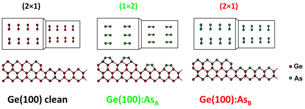
which has important consequences for GaAs nucleation [104–107]. The most relevant properties of Ge(100):As surfaces refer to the preferential As dimer orientation, the height of steps, and the atomic configuration at the step edges [110,111]. In analogy to Si(100) [113], As atoms adsorb on the Ge(100) surface and form As dimers, oriented either
parallel or perpendicular to the step edges. Here, we denote terraces of type A with (1×2) reconstruction as Ge(100):AsA (with As dimers aligned perpendicular to the step edges), and terraces of type B with (2×1) reconstruction as Ge(100):AsB (As dimers parallel to the step edges), as depicted in Fig. 9. Ge(100):AsA can be regarded as a surface where As is adsorbed in an additive fashion, whereas As may adsorb by displacing Si dimers at a Ge(100):AsB surface. According to Refs. [114–117], the displacing AsB adsorption leads to a lower surface energy configuration on Si(100), while the additive AsA adsorption represents a metastable structure. However, kinetics as well as energetics have to be considered to understand the step and domain formation. Ref. [113] highlights the impact of the preparation route on the resulting domain and step structure on vicinal Si(100):As.
STM measurements revealed the dependence of dimer orientation on the timing of arsenic exposure and subsequent substrate annealing sequence, as well as on actual values of the As4 flux and the exposure temperature.
Ge As
Ge(100):As
AGe(100):As
B(2×1)
Ge(100) clean
(1×2) (2×1)
Fig. 9: Schematic drawing to illustrate the effect on As adsorption on the vicinal Ge(100) surface
McMahon and Olson [110,111] studied the arsenic-exposed vicinal Ge(100) surface prepared in MOCVD environment in great detail by STM. As passivates the Ge(100) substrate leaving the surface chemically unreactive, so the surface remains clean in UHV for some days. Process temperature, source, and partial pressure of arsenic are important parameters for the Ge(100):As surface preparation. In MOCVD ambient, As can be supplied either directly via precursors such as AsH3 and tertiary-butyl-arsenic (TBAs), or indirectly as background As4 originating from the reactor environment covered by As
precursor fragments. The sublimation temperature of solid arsenic is 878 K, however, As compounds already volatilize from GaAs at lower temperatures [104]. At typical annealing temperatures around 920 K the presence of background As4 has to be considered to understand the step formation. AsH3 annealing may induce significant step bunching and ridge formation due to etching of the Ge surface dependent on temperature and partial pressure [110,111]. Most As/Ge steps are reconstructed resulting in a variety of different step reconstructions, which can be separated into two types, “single-row”, and
“double-row” steps. The formation of the step reconstruction depends on the sample preparation, too. Annealing at temperatures around 920 K in either AsH3 or background As4 result in (2×1) and (1×2) majority domain Ge(100):As surfaces, respectively, which deviate in step structure.
GaAs growth studies on Ge(100) [104], [106] indirectly showed the crucial influence of the surface preparation by As exposure on the quality of the subsequent GaAs nucleation layer. Ting and Fitzgerald [104] revealed a 90° sublattice rotation of the GaAs film grown on differently prepared Ge(100) surfaces in MOCVD ambient. Based on literature they discussed the sublattice rotation as an effect of the initial Ge(100):As domain structure, i.e. nucleation of GaAs on Ge(100):AsA and Ge(100):AsB. The formation of single domain Ge(100):As substrates significantly reduced the APD content and, as a consequence, the parallel resistance in subsequently grown GaAs solar cells [106].
P termination of the Ge surface should be obtained prior to nucleation for state-of-the-art GaInP on Ge heteroepitaxy in MOCVD [108] and [109]. Phosphine (PH3) and tertiarybutylphosphine (TBP) are the two main P precursors used in MOCVD systems.
Annealing under PH3 at 573–720 K in low pressure CVD systems leads to P termination of Ge(100) surfaces by one atomic layer [118]. LEED analysis of a P-terminated Ge(100) surface with 2° offcut prepared by PH3 exposure in MOCVD ambient shows a (9×2) surface reconstruction [108]. In contrast to AsH3, PH3 does not etch the Ge surface [119].
The influence of annealing under TBP on the Ge(100) surface is still unclear.
2.4 Experimental background
2.4.1 Metalorganic chemical vapor deposition
Metalorganic chemical vapor deposition (MOCVD) represents a flexible deposition technique for thin layers in the range of a few nanometers up to several micrometers. A great advantage of MOCVD is the ability to use a large variety of elements in the form of specially synthesized molecules, so-called precursors, for layer growth. In principle, precursors are transported by a highly purified carrier gas into the reactor at temperatures from 670 to 1200 K, where they decompose thermally and the elements are deposited on the heated substrate surface. Complex processes lead to growth of pure material layers which requires suitable process parameters. MOCVD is used for growth of metals (Al, Cu, FeTi), oxide compounds for optical coatings, sensors, and superconductors, as well as a large variety of semiconductor materials. For the growth of semiconductor materials, the term metalorganic vapor phase epitaxy (MOVPE) is also commonly used. Here, the monocrystalline structure is maintained during growth.
The principle of MOCVD was shown first by Manasevit and Simpson [120,121] in 1968/1969 for the growth of GaAs. Typical process pressures are in the range of 10 to 1000 mbar. Due to the high reproducibility of III-V compound semiconductor epitaxy and high throughput, MOCVD quickly became a well-established industrial technique for the growth of III-V semiconductor devices. High scalability made MOCVD superior over UHV-based techniques such as molecular beam epitaxy (MBE). The applied pressures during MOCVD preparation enable easier sample handling compared to UHV-based MBE growth. However, growth processes in MOCVD environment are less understood, since the growth reactions are much more complex. Here, reactions in the vapor phase, reactions on the substrate surface, as well as reaction with reactor residues from earlier deposited material have to be considered. Additionally, the presence of a process gas complicates analysis of the surface by standard UHV-based surface science tools.
In this work, an AIXTRON AIX200 MOCVD reactor was used for the sample preparation, a horizontal low-pressure reactor, which is specially equipped for surface analysis (see Fig. 10): optical in situ probes monitor the sample surfaces during MOCVD preparation, and a MOCVD-to-UHV transfer system enables contamination-free transfer of samples to UHV-based surface science tools. By correlation of results from surface science tools to characteristic in situ RA spectra, we achieved in situ control of sample surface preparation in dependence on the process parameters. Therefore, the samples are mounted on molybdenum sample carriers which enable transfer into UHV environment.
In situ monitoring of the sample by RAS or a curvature and pyrometry probe (Laytec EpicurveTT) is provided by an optical view port at the reactor glass tube which consists of strain-free glass and an opening in the liner glass.
Fig. 10: (a) Precursor source with bubbler and mass flow controllers; (b) schematic drawing of the MOCVD setup with UHV transfer system used in this work; (c) side view of optical view port and MOCVD reactor (modified after [122,123]).
Fig. 10 shows a schematic drawing of the MOCVD setup. H2 and N2 serve as carrier gases, which are purified in a palladium cell or a getter column, respectively. In this work, the III-V precursors tertiarybutylphosphine (TBP), triethylgallium (TEGa), trimethylindium (TMIn), and tertiarybutylarsine (TBAs) as well as silane (10% SiH4, diluted in H2) are used. Hydride sources are supplied in gas bottles. The III-V precursors are stored as liquid or solid metalorganic compounds at constant temperature and pressure
in so-called bubblers. In a bubbler, the purified carrier gas streams through the metalorganic compounds and carries them into the reactor. To avoid pre-reactions, group III and group V precursors are conducted in separate pipes (lines) and are mixed in the reactor afterwards. Here, the MO-compounds decompose by thermal activation at the sample. Samples are placed on a graphite susceptor which is heated by IR lamps. The process temperature is measured by thermocouples inside the susceptor block. Typical process temperatures for III-V layer growth are in the range of 750 to 1000 K. After decomposition of the precursor molecules, the atoms of the group III and V elements diffuse to the substrate surface and incorporate according to the crystal structure of the substrate material. Carrier gas and source flow into the reactor is adjusted by so called mass flow controllers (MFC). Fig. 10(a) illustrates the principle of a bubbler. The source flow qsource from the bubblers is set by the pressure MFC which controls the pressure pbubbler in the bubbler by the incoming and outgoing carrier gas. The “push” MFC stabilizes the flow into the reactor. The partial pressure pp of a precursor in the reactor is given by
vapor bubbler
reactor vapor
total source
P p p
p p q
p q
−
⋅ ⋅
= , Eq. 4
where qtotal is the total flow of all gases into the reactor, preactor the total pressure in the reactor and pvapor the vapor pressure of the precursors in the bubbler.
2.4.1.1 MOCVD-to-UHV transfer system
In order to study the MOCVD-prepared samples with UHV-based surface sensitive techniques, our MOCVD reactor is equipped with a UHV transfer system. It consists of an interim chamber, which is connected to the MOCVD reactor, a main UHV chamber, a transfer rod for sample handling, and a mobile UHV transfer chamber to access other UHV analysis chambers (see Fig. 10). MOCVD reactor and all UHV chambers are separated by several gate valves. Baking of the whole UHV system at 120 °C for 10 h and
pumping via the turbo molecular pump of the main chamber leads to pressures p ≤ 4∙10-10 mbar.
At the end of sample preparation, the MOCVD reactor is evacuated to pressures around 1 mbar, and plate valves between mobile chamber, interim chamber and main UHV chamber are closed before transfer. The reactor gate is opened when the pressure between reactor and interim chamber is balanced. After transfer of the sample to the interim chamber, the vent to the main chamber is immediately opened. Within 30 s, the pressure in the interim chamber, where the sample is located, is reduced below p ≤ 2∙10-9 mbar.
After another 5 min of evacuating with the help of a LN2-cooled cold trap, the pressure is below p ≤ 5∙10-10 mbar. When the sample is located in the mobile UHV chamber, all valves are closed and the sample can be transferred to various surface science instruments. A battery powered ion getter pump maintains a pressure of about p ≤ 5 ∙ 10-10 mbar in the mobile UHV chamber.
2.4.2 Reflection anisotropy spectroscopy
Reflection anisotropy spectroscopy (RAS), also known as reflection difference spectroscopy (RDS) is a non-destructive optical probe of surfaces which can be applied in different environments, e.g. in MOCVD. RAS measures the difference in reflectance (Δr) between two orthogonal directions in the surface plane (x, y) of complex Fresnel reflection amplitudes r normalized to the mean reflectance (r) in near normal incidence configuration of plane polarized light:
) r r (
r r r
Im r r i
Re r r
r
12
y x
y x
+
= −
+
= ∆ ∆
∆ . Eq. 5
On (100) semiconductor surfaces, the two orthogonal directions are chosen as x = [011]
and y = [011], consequently, the RAS signal measured in this work is defined as:
) r r (
r 2 r
r r
[011]
1]
1 [0
[011]
1]
1 [0
+
= −
∆ . Eq. 6
In the direction of these optical axes, ideal cubic crystals are isotropic and induce no RAS signal. Optical anisotropies mainly originate from the microscopic structure of the surface where the symmetry may be reduced due to surface reconstruction, atomic steps, or adsorbates. However, minor contribution to the RAS signal may originate from non-linear effects in the bulk such as defects or doping [124], and from buried heterointerfaces [26,125,126].
Although, RAS can be applied to many material systems, it is mainly established as a probe for single crystal surfaces. The interpretation of RAS signals from single crystal surfaces is difficult due to various contributions from the surface. Theoretical calculations of RA spectra have to regard the optical response of the surface, which depends on the complex dielectric function of both the surface region and the bulk. Since calculation of the dielectric function from first principles is rather complicated, only a limited number of theoretical studies of RA spectra of some surfaces exists, based on density-functional theory in the local-density approximation (DFT-LDA) (e.g.: [22,24,33,35]). Another successful approach is based on modeling of the RAS signal by different contributions (bulk, interface, surface) even without a detailed understanding of the optical response [26,126]. Also, comparison between RA spectra and experimental results from other surface-sensitive analysis tools such as STM, LEED, XPS, PE, enabled identification of different contributions to the spectra [127].
In the 1980s, Aspnes et al. [128] reported on the potential of RAS as a non-destructive optical probe of semiconductor surfaces. The need for control of substrate surfaces during preparation in different semiconductor growth systems pushed the development of RAS as in situ probe [20,21,129].
In this work, a RA spectrometer from the company Laytec (EpiRAS200) was used which features a phase-modulated RAS setup according to Aspnes [128]. Fig. 11 shows a
schematic sketch of the RAS setup. The light of a Xenon-arc-lamp is linearly polarized by a polarizing Rochon prism. It is focused onto the sample surface at near normal incidence in a 45° angle with regard to the anisotropic optical axes in the surface plane. In case of an anisotropic surface, the reflected light is elliptically polarized. The elliptically polarized light passes through a photo-elastic modulator (PEM), where it is phase modulated. In an analyzing prism, the phase modulation of the light signal is converted in an intensity modulation. The light is detected in a Si photo-diode in combination with a grating-monochromator. The measured modulated signal is processed in the connected electronics which includes a lock-in amplifier for analysis of the small RAS signals in the range of ± 5∙10-3. Details on the RAS signal processing can be found in Ref. [130].
Fig. 11: Principle of the RAS setup according to Aspnes et al. [128].
The optical path of the RAS system used in this in this work is presented in Fig. 12.
Spherical mirrors and a beam splitter direct the light on the sample in normal incidence.
An anti-wobble mirror (AWM) is used to compensate tilt in the optical path. At the
![Fig. 7: Side view of the different surface reconstructions induced by adsorption of atomic hydrogen (after [69])](https://thumb-eu.123doks.com/thumbv2/1library_info/5614120.1691764/28.892.240.688.512.748/fig-different-surface-reconstructions-induced-adsorption-atomic-hydrogen.webp)
![Fig. 8: (a) Ball and stick model of S A -, S B -, D A -, and D B -type steps of the Si(100) surface according to Chadi [15]](https://thumb-eu.123doks.com/thumbv2/1library_info/5614120.1691764/32.892.158.788.228.601/fig-ball-stick-model-steps-surface-according-chadi.webp)
![Fig. 11: Principle of the RAS setup according to Aspnes et al. [128].](https://thumb-eu.123doks.com/thumbv2/1library_info/5614120.1691764/43.892.237.625.471.948/fig-principle-ras-setup-according-aspnes-et-al.webp)
![Fig. 12: Optical path of a Laytec EpiRAS 200 system (taken from [130]).](https://thumb-eu.123doks.com/thumbv2/1library_info/5614120.1691764/44.892.321.579.380.818/fig-optical-path-laytec-epiras-taken.webp)
