MAX-PLANCK-INSTITUT FÜR PHYSIK
WERNER-HEISEBERG-INSTITUT
MPI-PhE/2002-21
Radiation Damage in Structured Silicon Semiconductor Detectors
Gerhard Lutz Max-Planck-Institut für Physik
for the MPI Semiconductor Laboratory, München
Invited talk presented at the IEEE Nuclear and Space Radiation Effects Conference Phoenix, Arizona, July 15-20, 2002
Abstract
The basic mechanisms of radiation damage in silicon detectors and their consequences on detector performance are described. This is done for two very different applications: spectroscopic imaging detectors as used in X-ray astronomy and position measuring tracking detectors which have to work in the extreme radiation environment of presently constructed particle colliders. The areas most prone to damage are identified and suggestions are given for improving the design or altering the concept.
80805 München – Föhringer Ring 6
Radiation Damage in Structured Silicon Semiconductor Detectors
Gerhard Lutz for the MPI Semiconductor Laboratory, München
Abstract
The basic mechanisms of radiation damage in silicon detectors and their consequences on detector performance are described. This is done for two very different applications: spectroscopic imaging detectors as used in X-ray astronomy and position measuring tracking detectors which have to work in the extreme radiation environment of presently constructed particle colliders. The areas most prone to damage are identified and suggestions are given for improving the design or altering the concept.
Keywords: Semiconductor detectors, Radiation damage, X-ray Astronomy, Particle physics, Silicon strip detectors, XMM, XEUS, DEPFET, pixel detectors
I. INTRODUCTION
Radiation damage has been studied extensively in the frame of electronics. It is also a subject of elaborate investigations in the context of semiconductor detectors. This is the case in particle physics where detectors have to withstand the harsh radiation environment of high luminosity particle colliders. Radiation damage at much lower dose is of relevance in space based X-ray observatories where detectors are exposed to cosmic radiation, to particles produced in solar flares and – depending on the satellite orbit - to the radiation belt. The high vulnerability with respect to radiation is due to the sophisticated structures of the detectors which have to provide simultaneously precision images with very high resolution spectroscopic information. The relative importance of damage mechanisms in detectors differ in many ways from that be in electronic devices. Thus the methods of improving radiation hardness of detectors also deviate from those used in
electronics.
The talk will review the mechanisms of radiation damage in silicon radiation detectors taking as a basis the observed and well parameterized changes in the material properties of silicon and silicon dioxide under exposure to radiation.
Particular emphasis will be given to structured
semiconductor detectors such as silicon strip detectors and X-ray CCDs for which device simulations and experimental results will be presented.
II. BASICSEMICONDUCTORDETECTORS The simplest semiconductor detector is a reverse biased diode as shown in figure 1. In this picture we have included already some complications at the fringe which are due to the finite size of the diode. A shallow highly doped p-region is produced by boron ion implantation into a lowly doped n- type silicon wafer. The rim of the wafer on the diode side is covered by thermally grown oxide and the backside with a highly phosphor doped n-type layer. This n+ layer allows the operation of the detector in over-depleted mode.
Signal charges (electron-hole pairs) generated for example by absorption of a X-ray photon are separated by the electric field, the electrons moving to the n+-side, holes to the p+ side, thus producing an electric signal which can be amplified and detected.
Problems - which can become much more severe with radiation damage - are encountered already here. They are due to the undefined boundary conditions on the outer oxide surface and the positive charge always present in the oxide and at the oxide-silicon interface. Applying the bias voltage for a sufficiently long period to the detector, the outer surface of the oxide will attain a potential distribution varying between the values applied to the n+ and p+ contacts. The form of this distribution is to some degree unpredictable as it is determined by the surface resistance on the outer oxide surface which may depend on minute rests of unknown material, on humidity and other conditions.
Fig.1: Simulation of potential distribution inside a fully depleted diode detector.
This unpredictability is also the source of instabilities which often occur only hours or days after application of the bias voltage
In this simulation the assumption has been made that the outer oxide potential is everywhere that of the backside n+
contact. The following observations are made: an electron accumulation layer forms underneath the oxide producing a very high field at the edge of the diode. This field can lead to avalanche multiplication and electrical breakdown. The problem already present before irradiation can be alleviated by the introduction of guard rings which define a graded potential on the oxide.
III. DEFECTSINSILICON
Defects in Silicon are already present before irradiation.
Irradiation creates additional defects. The simplest and most common defects are point defects, causing localized energy states within the band gap (Fig. 2). Its principal consequences on material properties will be sketched in the following.
Deep level defects are often only partially ionized. In thermal equilibrium their ionization probability is determined by the position of the Fermi-level. Thermal equilibrium considerations allow the derivation of a relation between capture and emission probabilities of charge carriers. Emission probabilities decrease exponentially with the distance from the corresponding band gap. Thus, defects substantially above mid-gap will essentially interact only with the conduction band, those below mid-gap with the valence band. Their main effect is trapping, capture and delayed release of charge carriers – as long as there are carriers available for capture. This is not the case in the space charge region. There the defects appreciably above mid-gap will emit an electron and stay in their more positive state; those below in their more negative state. Donors appreciably below mid-gap and acceptors appreciably above remain neutral. Defects close to mid-gap are able to emit alternatively electrons and holes and are thus responsible for leakage current generation in the space charge region.
The situation becomes somewhat more complicated when the density of deep level defects (traps) exceeds
substantially that of the original dopands. Consider for example a (radiation induced) acceptor state slightly above mid-gap in an originally n-doped semiconductor. Before irradiation the Fermi-level is assumed to lie above the defect level. The radiation induced defect states will be negatively ionized and the Fermi level moves downwards so as to reduce simultaneously the electron concentration and the ionization degree of the defect in order to conserve overall charge neutrality. Thus, at very high irradiation the Fermi level arrives a few times kT below the defect level near or even below mid-gap and the conductivity of the neutral bulk is close to that of an intrinsic semiconductor. On the other hand we will arrive at a very large space charge when the charge carriers are removed through application of an external voltage as is the case in a reverse biased diode.
Then the charge state of the defect is determined by the relative emission probabilities for electrons and holes. Thus high space charge density in depleted region is expected despite the high resistance of the non-depleted bulk.
The situation is somewhat more complicated for defects with more than two charge states or more than one energy level respectively.
Let us now consider the effects of point defects in detectors and in electronics:
Trapping is a source of low frequency noise in electronics.
As an example its role in FETs is illustrated in Fig.3. A trap located in the fringe region of the channel captures an
electron. which then induces a positive charge in the channel, thus reducing the channel current by a discrete amount which only depends on the position of the trap in the device. Traps close to the channel end will cause larger steps than those close
Fig.2: Band model description of simple deep level point defects
Fig.3: Generation of noise by trapping and detrapping of electrons in at trap located in the vicinity of the channel.
The trapped electron induces a positive charge in the channel and the transistor current changes between two fixed values with random time intervals and thus is called “Random Telegraph (RTS) Signal”. (After Kandiah et al. 1989 [1])
to the source. Once the electron is released again, the original current is restored. The randomness of capture and release times leads to a Lorentzian noise frequency spectrum which is constant at low frequency and falls with 1/f2 at high frequencies (Kandiah 1981, 1989 [1], [2] ).
In detectors the effect is trapping of part of the signal charge during charge collection and delayed release thus leading to a deformation of the time structure of the prompt signal. In detectors where the signal charge is not read promptly but is stored before being transferred to an output node, trapping leads to a loss respectively a wrong position assignment of part of the signal charge. This is the case for example with CCDs.
In electronics increase of Generation/Recombination is important for JFETs and bipolar transistors. It leads to a rise of gate leakage current in JFETS and a fall of current gain of bipolar transistors. In detectors the principal effect is an increase of detector leakage current.
Change and increase of space charge is the subject to which most attention has been given in the detector community in recent time. This is due to applications in the high radiation environment of presently built and planned particle colliders.
While this subject is of minor importance in electronics, in detectors it leads to the necessity to operate detectors at very high bias voltage which leads to problems with electrical breakdown and – in connection with the leakage current increase – to cooling requirements and thermal instabilities.
IV. DEFECTS OF OXIDE AND INTERFACE
This is a subject on which interest of the electronics community has centered. Here a short simplified summary of the damage mechanisms:
Thermally grown oxide is not a single crystal and therefore a large number of defects are already present before irradiation.
Their highest concentration is in the transition region between silicon and oxide. Ionizing radiation produces electron hole pairs. Electrons are rather mobile in oxide and have a high
chance of diffusing towards the conducting silicon or the outside surface, while holes are rather low mobility and a large chance to be trapped at the
defects in the oxide. Saturation of positive oxide charge buildup is reached when all traps are occupied by holes. Traps at or close to the interface have the additional property that their charge state can be changed by the presence of electrons or holes at the silicon surface. These interface states have a continuous defect energy level distribution across the silicon band gap. They may also show an amphoteric character. This means that they can assume several charge states.
In detectors the positive oxide charge buildup will lead to an increase of electrical field strength and connected with that to a risk of electrical breakdown. Interface state will trap charge carriers and thus reduce surface mobility. Furthermore they will create surface generation current in case that the depletion region extends all the way towards the oxide-silicon interface.
V. PARAMETERIZATION OF SI-PROPERTY CHANGES
Defect formation by irradiation is a rather complicated process which involves various intermediate stages of defect types which are changed for example by capture of additional vacancies. The processes are still not known sufficiently well.
Therefore for most practical purposes the material property changes are parameterized as a function of the irradiation dose. Scaling from one type of irradiation or from one energy to another is usually done by applying the NIEL (Non- Ionizing Energy Loss) hypothesis as shown in Fig. 4.
Figures 5-7 show volume generated current, space charge density and inverse trapping time parameterized as function of NIEL. These plots have been corrected for self annealing.
Annealing is a process which describes the effects of breaking up defect complexes with subsequent healing (for example by recombination of Si-interstitial with a vacancy) or reformation of new complexes. Annealing is strongly temperature dependent and occurs also at room temperature after the end of the irradiation. While the leakage current (Fig.8)decreases continuously, the space charge density (Fig. 9) rises again after the initial fall. This rise is also called reverse annealing.
Fig.4: Energy dependence of non-ionizing energy loss in silicon for various types of irradiation.
(After Vasilescu 1989 et al. [3] )
Fig.5: Fluence dependence of the volume generated current. Electrons are much less damaging than hadrons. (After Wunstorf 1992 [4] )
VI. RADIATION DAMAGE IN SPECTROSCOPIC
DETECTORS
Spectroscopic detectors are effected by radiation damage much earlier than position-only sensitive detectors. We will discuss damage and ways to minimize them on the example of focal detectors as used in X-ray astronomy.
Those detectors measure simultaneously position and energy of impinging X-ray photons with energy typically in the range of 150 eV to 20 keV.
CCDs are used for this purpose in two missions, the US Chandra [6] and the European XMM/Newton [7] space based X-ray observatories. Fig. 10 shows the
XMM/Newton observatory with its three X-ray mirror telescopes. The principle of the telescopes is shown in Fig.11. X-rays impinging at glancing angle are reflected two times on a combination of parabolic and hyperbolic mirrors and focused on a CCD focal detector. MOS type CCD detectors are used at Chandra and two of the three X-ray telescopes of XMM/Newton. The third mirror
telescope of XMM is equipped with a new type of CCDs which – besides other important advantages in this application – is more radiation hard. than MOS CCDs.
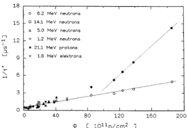
Fig.7: Fluence dependence of inverse trapping time.
(After Wunstorf 1992 [4] )
Figure 10: The XMM/Newton Observatory carrying three Wolter type X-ray telescopes and an optical telescope.
Fig. 8: Annealing of leakage current at room temperature. (After Wunstorf 1992 [4] )
1 10 100 1000 10000
annealing time at 60oC [min]
0 2 4 6 8 10
∆ Neff [1011cm-3]
NY,∞ = gY Φeq
NC NC0 gC Φeq
Na = ga Φeq Na = ga Φeq
Fig. 9: Annealing and reverse annealing of radiation induced space charge at elevated temperature. (After Lindstroem 2002 [5] )
Fig.6: Fluence dependence of space charge density.
The originally n-doped wafer changes space charge sign (type inversion) before it rises continuously with irradiation. (After Wunstorf 1992 [4] )
The principle of a MOS CCD is shown in Fig.12. Signal electrons created by ionization assemble in potential maxima at the Si-SiO2 interface created by the transfer gates. Periodic variation of their potential drives the charge towards the readout anode.
Such a device will not only work badly due to the presence of potential maxima in the regions between the non- overlapping gates. It will also be deteriorating strongly by radiation induced interface traps which will not only create surface generated current adding to the signal charge but in addition trap electrons along their transfer to the anode. The latter problem is cured in buried channel CCDs (Fig.13) the now standard technique. An additional n-type surface doping keeps the electrons at a distance from the surface.
Due to the large number of transfers needed to move signals from one end of the device to the readout anode, charge transfer inefficiency is the most vulnerable property of CCDs under irradiation. In fact, the MOS CCDs flown on Chandra
Fig.14: Operating principle of a pn-CCD. The wafer is depleted from pn-junctions on both surfaces of the wafer. The potential maximum close to the top surface is modulated by the diode like transfer registers. Their periodic potential variation moves the charge towards the readout anode. Surface generated electrons assemble below the oxide and are drained sideward (parallel to the transfer register towards a clear contact.
Fig12: Principle of a three phase MOS CCD Figure 11: Principle of a Wolter type X-ray telescope.
X-rays impinging on the mirror with very shallow angle are reflected twice on a combination of a parabolic and a hyperbolic mirror. Many nested mirror shells cover a reasonable solid angle
Fig.13: Principle of buried channel CCD. The charge is transported in a depth of roughly 0.5 micron.
Fig.15: Quantum efficiency of pn-CCD as function of X-ray energy
suffered already severe radiation damage within a few revolutions of the earth when crossing the radiation belt.
This damage was however not due to oxide damage by ionizing irradiation but by protons in the 100 keV range damaging the silicon crystal in the charge transfer depth region.
The third telescope on XMM is equipped with a pn-CCD [8], a device developed from scratch for this purpose. The operating principle is shown in Fig. 14.Compared to front illuminated MOS-CCDs it has already before irradiation several important advantages in the described application:
sensitivity over the full 300 micron bulk leading to extension of energy range at the high end; thin
homogeneous radiation entrance window on the backside leading to high quantum efficiency to lowest energy as seen in Fig.15. Two main reasons are responsible for the
improved radiation hardness: the absence of MOS structures and therefore surface generated currents (charge generated below the oxide between the registers is drained along the surface towards the side perpendicular to the transfer direction); the most sensitive charge transfer region is shielded by the silicon bulk against low and medium energy hadrons as the ones causing the Chandra performance deterioration.
The pn-CCDs have undergone a variety of irradiation tests with different types and energies of irradiation as well as changes in operation condition as for example temperature and driving pulse height and timing. Fig.16 gives a demonstration of the effect of very bad charge transfer efficiency which is a result of irradiation with 10 MeV protons at a level (1.9 109 cm-2) exceeding largely that
expected in orbit and choosing in addition very unfavorable operating conditions.
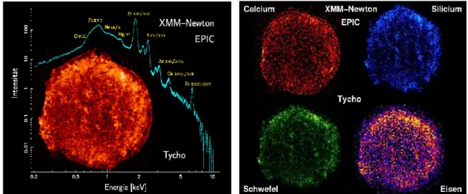
After more than two years operation in orbit the XMM pn-CCDs radiation damage is almost unnoticeably small. To demonstrate the quality of information obtained with this device, a the X-ray image and energy spectrum of Tycho Brahe’s supernova remnants is shown in Fig. 17 together with the element decomposition.
As charge transfer inefficiency is the dominant effect in radiation damage of CCDs, one may wonder if one cannot build imaging detectors with same imaging qualities that avoid the transferring charge altogether. A concept invented already in 1985 by Kemmer and Lutz [9] makes this possible. Fig. 18 shows this concept. A (MOS or JFET) transistor is located on a fully depleted bulk with the help of diode like structures on both wafer surfaces and an n+ type clear contact. Signal charge created by ionizing radiation assembles in a local potential maximum below the transistor gate and increases the
conductivity of the channel by influence. the signal charge is removed by a large positive pulse applied to the clear contact.
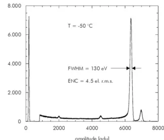
Fig. 19 demonstrates the very good spectroscopic performance obtainable with such a device. From the width of the Fe55 line at 5.9 keV one deduces an electronic rms noise value of 4.5 electrons.
Fig 17: X-ray image of the remnants of the supernova observed by Tycho Brahe in 1572. The overlaying energy spectrum allows an element decomposition.
Fig.16: Demonstration of effect of charge transfer inefficiency operating a heavily irradiated pn-CCD at very unfavourable conditions of timing and
temperature. The 5.9 and 6.5 keV lines of an Fe55 source fall exponentially with the number of transfers.
Simultaneously the following pixel pick up the signal charge lost in the transfer.
Covering a large area with DEPFETs and connecting them in the way shown in Fig. 20 one can read and subsequently clear the device line by line. This way all the device with exception of the currently read line are permanently ready for collection of the image. This without power consumption and no charge transfer is needed as the information is read at the position of generation.
DEPFET pixel detectors are foreseen as focal imager in the proposed European XEUS X-ray observatory [10].
Prototypes are in production at the MPI Semiconductor Laboratory in Munich.
VII. POSITION SENSORS IN VERY HIGH RADIATION
Let us now turn to a radically different scenario. The development of very high luminosity colliders has lead to the requirement of unprecedented radiation hardness of detectors.
Radiation hardness in the sense that detectors have to keep functioning without catastrophic failure. A certain deterioration of charge collection capability and of noise increase is unavoidable due to the material property changes which can only be reduced to a limited degree by
technological means. Therefore the emphasis is on the structure of devices, anticipating in the design already the expected material property changes.
Looking at the typical hadron collider we have a fast buildup of the oxide damage reaching at few hundreds krad a saturation value for the oxide charge of roughly 3.1012 e/cm2. This occurs in parallel with the bulk damage which develops much more slowly and does not show saturation. In good approximation we therefore can consider the scenario of oxide damage as in the case of gamma irradiation followed by bulk damage.
We will discuss the problems on the example of double sided strip detectors built on n-type silicon. Before entering this field however, a remark on the mechanism which prevents catastrophic failure immediately after type inversion even on a simple diode.
Figure 18: The DEPFET detector-amplifier principle; cross section and device symbol
Fig 21: Simulation of a type inverted diode Fig.20: Circuit diagram of a DEPFET pixel detector.
The matrix arrangement of transistors allows individual or parallel row wise readout of the charge stored in the internal gates of the DEPFETs. Only those pixels being read consume power.
Fig. 19: Iron 55 energy spectrum measured with a single DEPFET transistor.
A. Survival of type inversion
Fig. 21 shows the potential simulation for a simple diode.
The properties of the damaged silicon are not correctly treated in this simulation. The type inverted silicon is just represented by a by a fairly high doped p-type silicon giving the same space charge density but improper behavior of the non depleted bulk. Furthermore the heavily damaged cut region is not treated properly. This region will connect the backside potential with the electron layer underneath the oxide a fact taken into account in the simulation. We notice that the rectifying junction has moved to the backside and that the electric field extends towards the cutting edge. The resulting surface generation current at this edge is also not part of the simulation. A qualitative picture on what is happening can be seen in Fig.22. Holes created at the cutting edge are trapped in deep level defects, thereby decreasing the electric field at the cutting edge and thus retarding the influx of further holes into the bulk. Also noticeable in Fig. 21 is the large voltage drop across the rim of the detector.
B. Strip detectors
Turning now to strip (and pixel) detectors we will concentrate on strip detectors with narrow strips and wide gaps. Such a configuration is often chosen in order to keep the capacitive load to the electronics small, thereby limiting the serial noise of the input amplifier. Although this is in principle desirable, it brings about some problems which are
often forgotten and can lead to disastrous consequences. We choose as example a double sided strip detector with 75 micrometer pitch and a strip width of 10 micron. As isolation method on the n-side we use p-doped electrically floating strips (p-stops), the method applied by most manufacturers despite the fact that it brings about several important disadvantages in comparison to the p-spray and
“moderated p-spray” technique as developed and used in our laboratory.
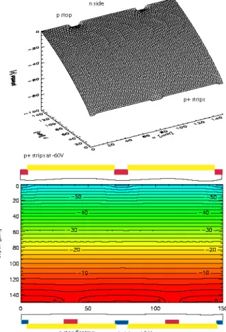
Fig. 23 shows a simulation of the potential distribution in a non-irradiated detector. A fairly smooth potential
distribution is observed similar to that of a diode. The largest electric fields are at the edges of the p-stops.
Looking now at the consequences of oxide damage, the situation arising at the beginning of the collider scenario we see in Fig. 24 a significant voltage drop across the oxide on
Fig 22: Mechanism for survival of a type inversion of a simple diode
Fig 23: Simulation of a non-irradiated double sided strip detector
Fig 24: Simulation of a gamma-irradiated double sided strip detector
the p-strip side. Even with the thin oxide of 200nm a voltage drop across the oxide on the p-side of 35V is observed. By this voltage - which grows linearly with the oxide thickness - the bias voltage has to be increased.
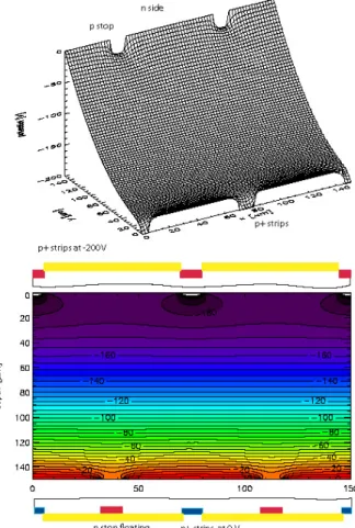
Fig. 25 shows the potential distribution of the 150 micron thick detector after proton irradiation leading to saturation in oxide charge of 3. 1012 cm-2 and a space charge
corresponding to 5. 1012 cm-3. A bias voltage of –200V has been applied . The following observations can be made:
• due to “type inversion” the high field region has moved to the n-side
• a low field region extends from the p-side fairly deep into the bulk (approximately half pitch size).
This is due to the electron layer underneath the oxide which can only be removed with very large bias-over-voltage.
• very high electric fields at the edges of the p-stops make the device prone to electrical breakdown C. Design considerations (how to avoid catastrophic failure)
After pointing out some problematic points with the wide gap strip and pixel detectors it is natural to ask how the effects of radiation damage in high radiation environment can be kept at a manageable level. We will leave aside in this discussion the partially successful attempts of material engineering as for example the introduction of oxygen into
silicon [5].
From the previous discussion it seems clear that the use of wide gap detectors by itself poses a problem. Small gap detectors are preferred whenever there is no overriding reason –as for example capacitance considerations - which enforce the wide gap solution. Here it should be noted that low capacitance can also be reached in charge division readout by the introduction of floating charge division strips. The p-stops on the n-side is a bad solution in any case as the n-strip isolation can also be reached by a moderately doped p-spray or even better by moderate p- spray doping.
A simulation with simple p-spray isolation on the n-side is shown in Fig.26. One notices a smooth potential
distribution, rather close to that of a simple diode on a p- doped substrate. No strong electric field strength are present after proton irradiation. The situation presented in Fig 26 however is not the situation with the highest field strength. That occurs in the non-irradiated situation where one has strong fields at the at the boundary between n- strips an p-doped compensation implant. This is a desirable situation however, as the worst, still manageable situation occurs at a time when the functioning of the device can be tested before putting it into first use. The situation can be improved further by diminishing the concentration of the compensation implant at the edges of the n-strips. This “moderated p-spray” isolation technique [11] has been developed at the MPI Semiconductor Laboratory.
One should also be aware of the fact that the perfect behavior after irradiation obtained in simulation is due to Fig 25: Simulation of a proton-irradiated double sided strip detector
Fig 26: Simulation of a “radiation hard double sided strip detector concept” after proton-irradiation: wide gap n-strips with p-spray isolation and small gap p- strips on the other wafer side.
the matching of the doping concentration in the compensation implant to the saturated oxide charge.
Strong over-compensation will be equivalent to using wide p-stops. Under-compensation will on first glance leave an accumulation layer which shortens
neighboring strips. This is however not the case as has been found experimentally and can be explained by the presence of radiation induced interface states [12].
Those interface states trap the electrons at the surface and prevent them from building a conductive layer.
The superiority of p-spray isolation of n-strips is demonstrated in experimental results obtained in the ATLAS pixel detector project presented in Figs. 2 and 28. Fig. 27 presents the much improved breakdown behavior after irradiation, Fig. 28 even more drastically the superiority when looking at the noise performance.
VIII. SUMMARY
The paper tried to point out some important aspects of radiation damage in (silicon) semiconductor detectors.
This was done by considering two typical situations occurring once for the case that the defect level concentration stays well below the original doping densities and in the second case that the defect concentration outweighs the original bulk doping. The effects of oxide damage plays also an important role in detector performance. In the following some conclusions will be drawn.
No general rule can be given for making detectors radiation hard. This depends very much on the task which the detector has to fulfill. Before concentrating on a particular device one should look at alternative concepts and weigh their relative usefulness giving special attention to the expected effects of radiation damage. Once a particular concept has been chosen, computer simulations taking into account the expected material changes should be performed. Here one should also consider the possibility of defect engineering which will not suppress radiation damage but may be able to improve to a certain degree some material properties (while possibly deteriorating some others).
Some specific suggestions were made for imaging
detectors in X-ray astronomy. In CCDs trapping during charge transfer is the prime effect for detector deterioration. This is most prominent in front illuminated MOS-CCDs as commonly used in present X-ray observatories. A large improvement is obtained with the back illuminated p-n CCD in one of the XMM/Newton telescopes. Strong further improvement is expected from the DEPFET pixel detectors foreseen for the planned European XEUS observatory. This detector avoids charge transfer readout altogether by using a new detector principle which also promises several other important advantages.
Detectors to be used in high energy particle colliders will be exposed to radiation which creates defect densities above that of original dopands of the detector grade silicon. Consequently the material properties at the end of the exposure will be dominated by these defects and not the original doping. The space charge of an original n-doped Si wafer becomes strongly negative while the conductivity of the non-depleted bulk is close to that of intrinsic silicon. As very high voltages have to be applied to deplete the detector these detectors are prone to electrical breakdown. Care has to be given in the design to prevent occurrence of high electric field regions as has been shown for some illustrative examples. The radiation increased leakage current in combination with the large bias voltage needed for depletion forces operation at low temperature. Low temperature simultaneously slows down “reverse annealing”, a further increase in negative space charge even after the end of irradiation. An additional way of retarding negative space charge buildup is the use of oxygen enriched silicon, a subject only mentioned in this paper.
bias [V]
current [µA]
pixel region guard ring region
0 200 400 600 800 1000
0 200 400 600 800 1000
bias [V]
current [µA]
pixel region guard ring region
0 20 40 60 80 100 120 140 160 180 200
0 200 400 600 800 1000
Fig. 27: Leakage current of two different pixel
detectors after same exposure to 55 MeV protons of the NIEL equivalent radiation dose of 1015 neutrons/cm2 Compare the hard breakdown of p-stop detectors at 600V bias (left} with the much lower leakage current and absence of breakdown up to 1000V of p-spray pixel detectors (right figure).
Fig. 28: Average pixel noise for the two pixel detectors after irradiation to 5. 1014 and 1. 1015 neutron/cm2 NIEL equivalent dose. The noise remains small in all cases for p-spay design (filled symbols). It is strongly increased at the lower dose and goes completely off scale for the higher dose at (2600 ENC) and above 300V bias.
References
[1] Kandiah, K. (1981) et al.: Proc. 6th Conf. on noise in physical systems, NBS Publication 614, U.S. Department of Commerce,1981.
[2] Kandiah, K. (1989) et al.:
“A physical model for random telegraph signal currents in semiconductor devices”. J. Appl. Phys. 66, pg. 937-948 (1989) [3] Vasilescu, A. (1998) et al.: “Fluence normalization based on NIEL Scaling hypothesis”, 3rd ROSE Workshop, DESY Hamburg, 12-14 February 1998, DESY Proc. 1998-2
[4] Wunstorf, R. (1992): “Systematische Untersuchungen zur Strahlenresistenz von Silizium-Detektoren fuer die Verwendung in Hochenergiephysik-Experimenten”, Ph.D. thesis, Universitaet Hamburg, 1992
[5] Lindstroem, G. (2002): “Radiation damage in Silicon detectors”; paper presented at the 9th European Symposium on Semiconductor Detectors, Elmau June 23-27, 2002; to be published in Nucl. Instr. & Meth.
[6] Weisskopf, M.C. et al.: “Chandra X-Ray Observatory (CXO): Overview”; Proceedings of SPIE Vol. 4012 (2000) pp 2-16
[7] Jansen, F. et al: “XMM-Newton observatory”; Astronomy and Astrophysics 365 (2001) L1-L6
[8] Strüder, L. et al: “The European Photon Imaging Camera on XMM-Newton: The pn-CCD camera”; Astronomy and Astrophysics 365 (2001) L-L26
[9] Kemmer, J. (1987) and G. Lutz: ''New semiconductor detector concepts''; Nucl. Instr. & Meth. A 253 (1987) 356-377 [10]ESA “X-ray Evolving-Universe Spectroscopy – The XEUS Science Case”; ISBN No 92-9092-548-5; European Space Agency, SP-1238 (March 2000)
[11] Richter R.H. et al.: “Radiation tolerance of detectors with p-spray isolation” paper presented at the 9th European Symposium on Semiconductor Detectors, Elmau June 23-27, 2002; to be published in Nucl. Instr. & Meth.
[12] T.P. Ma and P.V. Dressendorfer: “Ionizing radiation effects in MOS devices and circuits”, chapter 4, Wiley 1989