Weak localization and Raman study of anisotropically etched graphene antidots
Florian Oberhuber, Stefan Blien, Stefanie Heydrich, Fatemeh Yaghobian, Tobias Korn et al.
Citation: Appl. Phys. Lett. 103, 143111 (2013); doi: 10.1063/1.4824025 View online: http://dx.doi.org/10.1063/1.4824025
View Table of Contents: http://apl.aip.org/resource/1/APPLAB/v103/i14 Published by the AIP Publishing LLC.
Additional information on Appl. Phys. Lett.
Journal Homepage: http://apl.aip.org/
Journal Information: http://apl.aip.org/about/about_the_journal Top downloads: http://apl.aip.org/features/most_downloaded Information for Authors: http://apl.aip.org/authors
Weak localization and Raman study of anisotropically etched graphene antidots
Florian Oberhuber, Stefan Blien, Stefanie Heydrich, Fatemeh Yaghobian, Tobias Korn, Christian Sch€uller, Christoph Strunk, Dieter Weiss, and Jonathan Eromsa)
Institut f€ur Experimentelle und Angewandte Physik, Universit€at Regensburg, Universit€atsstr. 31, D-93053 Regensburg, Germany
(Received 12 August 2013; accepted 14 September 2013; published online 1 October 2013) We study a crystallographic etching process of graphene nanostructures, where zigzag edges can be prepared selectively. The process involves heating exfoliated single-layer graphene samples with a predefined pattern of antidot arrays in an argon atmosphere at 8208C, which selectively removes carbon atoms located on armchair sites. Atomic force microscopy and scanning electron microscopy cannot resolve the structure on the atomic scale. However, weak localization and Raman measurements, which both probe intervalley scattering at armchair edges, indicate that zigzag regions are enhanced compared to samples prepared with oxygen based reactive ion etching only.VC 2013 AIP Publishing LLC. [http://dx.doi.org/10.1063/1.4824025]
Graphene nanoribbons (GNRs),1–3as well as step edges on highly ordered pyrolytic graphite (HOPG),4–6were pre- dicted to show a high local electronic density of states, if these edges are along the crystallographic zigzag orientation.
For HOPG, this was demonstrated experimentally by scan- ning tunneling microscopy and spectroscopy.7,8An exciting property of the zigzag edge, which still remains to be con- firmed experimentally, is the spin-polarized edge state.2,3,9 Its observation is a challenging task, since edges cannot be defined by electron beam lithography (EBL)10 with atomic precision. Typical bottom-up processes, which, for instance, rely on organic molecules11 or growth on templated SiC surfaces,12and those which are based on breaking up carbon nanotubes (CNTs)13 can create crystallographically defined edges. These approaches, however, do not allow position control to an extent comparable to lithographic methods.
Crystallographically anisotropic etching is selective concerning the etching of carbon atoms located at different edges, and bears the potential to define armchair or zigzag edges without roughness on the atomic scale.14–23The etch- ing reaction can occur in a catalyzed14–17 or in a non- catalyzed form.18,20–23Only the latter allows position control of the edges via a lithographic patterning process prior to the anisotropic etching.18,20–22 Quality demonstration of edges obtained by anisotropic etching has focused on Raman spectroscopy18–22 and electron transport measurements of the ambipolar field effect.20–22The interpretation of Raman spectra acquired on crystallographically defined edges is based on the edge-orientation-sensitive elastic intervalley scattering of charge carriers between the K and K0 valleys.
Another way to probe intervalley scattering is electron trans- port measurements of the weak localization (WL) feature,24 however, to this day, no experimental data have been reported on anisotropically etched graphene.
We performed a crystallographically anisotropic carbo- thermal etching process similar to that reported in Ref.18on graphene antidot lattices25,26 patterned by EBL and reactive
ion etching (RIE) with an oxygen plasma. After discussing our carbothermal anisotropic etching process, we will present a comparative study of Raman and WL measurements on a set of samples with focus on intervalley scattering. Part of the samples in this study was not subjected to the anisotropic etch- ing process, but only patterned by EBL and RIE.25,26By ana- lyzing the intervalley scattering process in both types of samples by both methods, we can deduce that our anisotropic etch step predominantly generates zigzag edges, however, with varying edge roughness, which is still not well controlled.
Samples were prepared by exfoliation of natural graphite onto Si chips covered with a 300 nm oxide layer. By EBL and RIE, we defined square lattices of circular holes with diameter d40 nm and lattice constantsa140–450 nm in the flakes.
In a manner similar to Ref.18, samples were etched at a tem- peratureT8208C in a quartz tube reactor in a flow of Ar gas (purity99:9999%, O20:5 ppm) at ambient pressure.
During this anisotropic etching step, the antidots were grown from a circular to a hexagonal geometry and to diameters d100–150 nm (cf. Fig. 1). The samples on which we did not perform anisotropic etching were prepared with the same lattice constants, but antidot diameters d 40–165 nm. We performed scanning electron microscopy (SEM) and atomic force microscopy (AFM) to characterize the etching process.
In order to keep the samples clean, care was taken not to ex- pose the flakes to the electron beam of the SEM before con- ducting Raman or transport measurements. Raman spectra were recorded with 532 nm circularly polarized light. Details of the Raman setup are reported elsewhere.27In order to per- form four-point transport measurements, flakes were pat- terned into Hall bars by EBL and RIE, and contacts were fabricated by EBL and evaporation of Pd, Re, or Au with an adhesion layer of Cr or Ti. Transport data were recorded in He-cryostats at an AC of 10 nA, while the charge carrier den- sity was controlled via the back gate.
Anisotropic etching showed the best performance in a narrow temperature range around T8208C, with lateral etch rates20nmh for single-layer graphene, whereTdenotes the temperature of the outer wall of the quartz tube. In
a)Electronic mail: jonathan.eroms@physik.uni-regensburg.de
0003-6951/2013/103(14)/143111/5/$30.00 103, 143111-1 VC2013 AIP Publishing LLC
Ref. 18, the reaction was suggested to occur between gra- phene and the SiO2’s oxygen atoms. However, several obser- vations in our experiments are incompatible with this scenario. Experiments with multi-layer graphene and single- layer graphene in UHV or in a H2atmosphere suggest that the reaction involves gaseous O2with concentrations 0:5 ppm in the Ar atmosphere.28
For single-layer graphene, we observed a remarkable behavior, in line with reports on anisotropic etching with hydrogen plasma:22,23while etching was observed to be ani- sotropic for graphene two or more layers thick, it was iso- tropic for single-layer graphene, unless we applied a specific sample preconditioning step prior to etching. This precondi- tioning involves heating the samples toT8508C, with a stainless steel grid located upstream of the sample.28
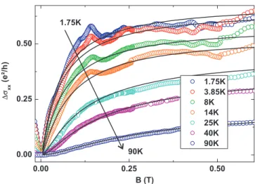
Now, we discuss the quality of anisotropically etched samples by analyzing the WL. WL is a phase-coherent effect, whose sign and amplitude in graphene depend on the inter- play of the phase-coherence length, the intervalley scattering length, and the intravalley scattering length. In particular, intervalley scattering occurs at armchair edges, making the effect visible.29–31 We measured WL for samples that have undergone anisotropic etching, and samples that have not, i.e., we compare WL for samples with lattices of hexagonal and circular antidots, respectively. In order to extract interval- ley scattering lengths from the WL peaks, we fitted the raw data to the theory24 according to the equation drðBÞ
¼phe2 F BBu F Buþ2BB
i
2FBuBþB
h i
for single-layer graphene, as shown in Fig. 2. Here, FðzÞ ¼lnðzÞ þwð0:5þz1Þ, Bu;i;¼4Deh s1u;i;, and s1 ¼s1w þs1z þs1i .wis the digamma function,Dis the diffusion constant, sudenotes the phase coherence time,sidenotes the interval- ley scattering time, andðs1w þs1z Þ1denotes the intravalley scattering time. The scattering lengths are related to the scat- tering times viaLu;i;¼ ffiffiffiffiffiffiffiffiffiffiffiffiffiffi
Dsu;i;
p . Performing the measure- ments at different temperatures allowed us to prove WL as the origin of the observed peaks, and to extract aLu/T0:5 dependence.25
Circular antidots would be expected to have roughly an equal amount of armchair and zigzag segments. Hexagonal antidots created by anisotropic etching can be terminated by zigzag or armchair edges. For antidots with zigzag edges, a lower amount of intervalley scattering events leads to an
increasedLi, and vice versa for armchair edges. In Fig.3, we plotLiextracted from data atT¼1:6 K for different single- layer graphene flakes with hexagonal or circular antidots.32 Different data points in part stem from different samples, in part from samples which were measured at different charge carrier densities. In Ref. 25, we found a linear relationship betweenLiand the spacinga–dbetween neighboring antidots (see sketch of the lattice in inset of Fig.4), which can also be seen in Fig. 3 for the data on circular antidots (blue data points). The data for anisotropically etched graphene show significant scatter. The highest values for Liat given values fora–dare observed for anisotropically etched samples, and reach up to 235 nm, whereas the lowest values forLiare pre- dominantly observed for samples with circular antidots. For comparison, values forLireported for graphene on SiO2with- out intentional defects lie in the range 250 nm–1lm.33,34 From this, we deduce that our anisotropic etching reaction favors the creation of zigzag edges, however, with varying edge quality. With our available microscopy methods, we could not resolve differences between anisotropically etched
FIG. 1. SEM images of single- (a), and bilayer graphene (b) after application of the preconditioning step and conducting the etching reaction. Anisotropic etching generated the hexagonal shape of the antidots and the flakes’ straight borders.
FIG. 2. Experimental data for different temperatures on the WL peak (circles), measured on a sample with anisotropically etched hexagonal anti- dots of diameter d¼100 nm patterned in a square lattice of constant a¼200 nm. The lines display fit curves according to Ref.24.
FIG. 3.Lifor a set of single-layer graphene samples with circular (blue color) and a set with anisotropically etched hexagonal antidots (red). Part of the samples with circular antidots was already reported in Ref.25. Lines in respective color display fits to each data set. The data point highlighted by a black circle around it stems from the measurement shown in Fig.2.
143111-2 Oberhuberet al. Appl. Phys. Lett.103, 143111 (2013)
samples with comparatively high or low values forLi. Hence, the anisotropic etching process must generate an edge rough- ness on a scale lower than our microscopy resolution limit of 3 nm for AFM and1.5 nm for SEM.
In addition to the WL data, we studied Raman spectra on single-layer graphene with anisotropically etched hexago- nal antidots, and single-layer graphene with circular holes.
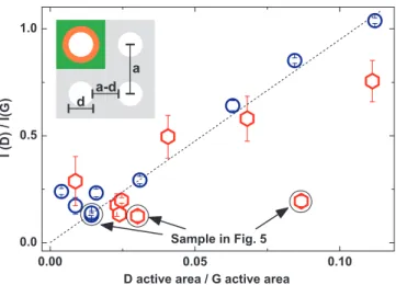
Intervalley scattering is responsible for the appearance of the defect, or D peak, in the spectrum of sp2-hybridized car- bon.30,31If there are no other significant scattering sources, such as defects, on the sample, the D peak intensity measures the amount of armchair edges within the area of the graphene flake, that is illuminated by the laser beam.35Anisotropically etched graphene edges have been studied with regard to the ratio of the D peak intensityI(D) over the G peak intensity I(G).18–22The G peak intensity measures the amount of sp2- hybridized carbon atoms within the illuminated sample area.
Perfect zigzag edges cannot generate a D peak, and, there- fore, the expected ratioIðDÞ=IðGÞwould be zero. The ratio IðDÞ=IðGÞfor circular holes with a roughly equal amount of zigzag and armchair segments would be expected to lie between that for zigzag and armchair edges. Further, the D and G peak intensities not only depend on the microscopical composition of the edges but also on the polarization of line- arly polarized light with respect to the edge orienta- tion.31,36,37The use of circularly polarized light in our setup, however, eliminates this effect.
In order to compare samples with different antidot lattice geometries, we consider their unit cell. Several antidot lattice unit cells are contained within the laser spot diameter of about 1lm. In each of them, the G peak is generated in the area covered by carbon atoms, i.e.,a2 ðd=2Þ2p. The mecha- nism for D peak Raman scattering involves a virtual state, which gives the process a certain lifetime related to a length scale of 4 nm via the Fermi velocity.38–40 Consequently, the D peak in each unit cell should be generated in an area
formed by a ring of width 4 nm around the antidot, i.e.,
½ðd=2þ4 nmÞ2 ðd=2Þ2pdp 4 nm (cf. Fig. 4). The ratio IðDÞ=IðGÞ should be proportional to the ratio of the areas activating the respective peaks. In Fig. 4, we plot the integrated intensity ratio41 vs. the peak activation area ratio for different samples. As expected, for samples with round holes, the graph shows a linear relationship (blue data points).
Compared to circular antidots, IðDÞ=IðGÞ-values for aniso- tropically etched antidots lie in the same range, or lower, at respective peak activation area ratios (red data points). As for WL, the edge quality of samples with comparatively high or low IðDÞ=IðGÞ-values cannot be distinguished with our mi- croscopic methods. This supports the conclusions that we drew from the WL data. The spectra for the anisotropically etched samples in Fig. 4with the lowest ratio ofIðDÞ=IðGÞ were acquired on one and the same flake and are displayed in Fig.5.
The Raman spectra shown in Fig.5(a)were recorded on a single-layer graphene flake between consecutive sample processing steps. Spectra were acquired for the sample in its pristine state, after definition of circular antidots by EBL and RIE, after sample preconditioning, and after two separate etching steps. The correspondingIðDÞ=IðGÞ-values in Fig.4 are marked by black circles and indicate high edge quality af- ter anisotropic etching. Since the lattice constant remains unchanged after the definition of antidots, not only the IðDÞ=IðGÞ-ratio is a viable measure of the edge quality but also the ratio of the integrated D peak intensity over the D active area. Fig.5(b)plots this ratio for four of the spectra in Fig.5(a). The data in Fig. 5(b)were normalized to the data point for circular antidots. According to the positions for the G and 2D peak,28the pristine flake shows a very high degree of doping.26,42–44Introducing circular antidots decreased the FWHM of the D and G peak, and shifted the D, G, as well as the 2D peak as an indication of a decreased degree of doping.
This might be due to a reduction of dopant adsorbates by the
FIG. 4. Integrated intensity ratiosIðDÞ=IðGÞvs. the ratio of peak activation areas. The dashed line is a guide to the eye. Legend and origin of the data are as in Fig.3. The inset shows a schematic of graphene (grey) patterned with an antidot lattice (white) with constantaand antidot diameterd. The orange-colored area displays the activation area for the D peak, the orange and green-colored areas together show the activation area of the G peak within one unit cell of the lattice, respectively. The data points highlighted by black circles stem from the spectra shown in Fig.5.
FIG. 5. (a) Raman spectra of a single-layer graphene flake between different stages of sample processing. Antidots were patterned in a square lattice of constanta¼200 nm. The diameterdfor round antidots was40 nm, pre- conditioning left it unchanged, and they were grown to 80 nm and 150 nm within the first and second anisotropic etching steps, respectively.
The three vertical lines mark the positions for the D, G, and 2D peak for the spectrum after the sample preconditioning step. The symbols on the right- hand side refer to the data points in Fig.5(b). (b) Plot of the normalized ratio between D peak intensity and the D active area for the spectra in (a) in their respective symbol and color.
liquid solvents involved in the processing. The precondition- ing step left the peak intensities unchanged, however, the peak shifts monitor a decrease of doping, which might be explained by the evaporation of dopant adsorbates from the flake at the elevated temperature. The reduction of the G peak intensity after consecutive anisotropic etching steps reflects the reduced carbon-covered area. Further, the first anisotropic etching step induced a reduction of the D peak in- tensity, as well as a reduction of the ratio of intensity over active area to roughly 25% compared to the spectrum for the circular antidots. However, application of a second aniso- tropic etching step to grow the antidots further led to an increase in D peak intensity, which should not occur for per- fect zigzag edges. On the other hand, while the absolute D peak intensity increases, the ratio of intensity over active area further decreases due to this second anisotropic etching step, as displayed in Fig.5(b). The successive decrease of the ratio of D peak intensity over D active area in Fig.5(b)due to anisotropic etching favors zigzag as dominating edge type.
The increase of D peak intensity due to the second aniso- tropic etching step, as well as the fact that D peak intensities are non-zero, is in line with edge roughness.
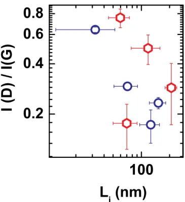
Finally, since both WL and Raman are sensitive to inter- valley scattering, we plot the Raman D-peak intensity vs.Li
from the WL fit for samples on which both measurements were performed. Fig.6indeed shows a correlation between those quantities.28 The large scatter in the data might be explained by considering that the WL-theory in Ref.24was derived for randomly distributed defects and its applicability is limited for antidot lattices. Another reason could be that Raman spectroscopy probes intervalley scattering at much higher charge carrier excitation energies compared to WL.
In conclusion, we performed anisotropic etching of single-layer graphene on SiO2at oxygen concentrations of 0.5 ppm. Anisotropic etching preferentially generated zig- zag edges with roughness between the atomic scale and 1.5 nm. This was demonstrated by studying the intervalley scattering process in WL and Raman measurements for a set of antidot samples, and by tracking the evolution of Raman spectra on a single flake after consecutive processing steps.
We also establish a correlation between the D-peak intensity in the Raman spectrum and the intervalley scattering length obtained from fitting the WL data.
We thank Jan Bundesmann for programming a WL fit- ting tool, Thomas Hofmann for performing the heating experiments in UHV, and gratefully acknowledge financial support by the DFG via SFB 689 and GRK 1570.
1K. Nakada, M. Fujita, G. Dresselhaus, and M. S. Dresselhaus,Phys. Rev.
B54, 17954 (1996).
2Y.-W. Son, M. L. Cohen, and S. G. Louie,Phys. Rev. Lett.97, 216803 (2006).
3Y.-W. Son, M. L. Cohen, and S. G. Louie,Nature444, 347 (2006).
4K. Kobayashi,Phys. Rev. B48, 1757 (1993).
5D. Klein,Chem. Phys. Lett.217, 261 (1994).
6M. Fujita, K. Wakabayashi, K. Nakada, and K. Kusakabe, J. Phys. Soc.
Jpn.65, 1920 (1996).
7Y. Kobayashi, K.-i. Fukui, T. Enoki, K. Kusakabe, and Y. Kaburagi,Phys.
Rev. B71, 193406 (2005).
8Y. Niimi, T. Matsui, H. Kambara, K. Tagami, M. Tsukada, and H.
Fukuyama,Appl. Surf. Sci.241, 43 (2005).
9M. Wimmer, I. Adagideli, S. Berber, D. Tomanek, and K. Richter,Phys.
Rev. Lett.100, 177207 (2008).
10M. Y. Han, B. Ozyilmaz, Y. Zhang, and P. Kim,€ Phys. Rev. Lett.98, 206805 (2007).
11J. Cai, P. Ruffieux, R. Jaafar, M. Bieri, T. Braun, S. Blankenburg, M.
Muoth, A. P. Seitsonen, M. Saleh, X. Feng, K. Mullen, and R. Fasel, Nature466, 470 (2010).
12M. Sprinkle, M. Ruan, Y. Hu, J. Hankinson, M. Rubio-Roy, B. Zhang, X.
Wu, C. Berger, and W. A. de Heer,Nat. Nanotechnol.5, 727 (2010).
13L. Jiao, L. Zhang, X. Wang, G. Diankov, and H. Dai,Nature458, 877 (2009).
14S. S. Datta, D. R. Strachan, S. M. Khamis, and A. T. C. Johnson,Nano Lett.8, 1912 (2008).
15L. Ci, Z. Xu, L. Wang, W. Gao, F. Ding, K. Kelly, B. Yakobson, and P.
Ajayan,Nano Res.1, 116 (2008).
16L. C. Campos, V. R. Manfrinato, J. D. Sanchez-Yamagishi, J. Kong, and P. Jarillo-Herrero,Nano Lett.9, 2600 (2009).
17L. Gao, W. Ren, B. Liu, Z.-S. Wu, C. Jiang, and H.-M. Cheng,J. Am.
Chem. Soc.131, 13934 (2009).
18P. Nemes-Incze, G. Magda, K. Kamaras, and L. Biro,Nano Res.3, 110 (2010).
19B. Krauss, P. Nemes-Incze, V. Skakalova, L. Biro, K. von Klitzing, and J.
H. Smet,Nano Lett.10, 4544 (2010).
20L. Xie, L. Jiao, and H. Dai,J. Am. Chem. Soc.132, 14751 (2010).
21R. Yang, L. Zhang, Y. Wang, Z. Shi, D. Shi, H. Gao, E. Wang, and G.
Zhang,Adv. Mater.22, 4014 (2010).
22Z. Shi, R. Yang, L. Zhang, Y. Wang, D. Liu, D. Shi, E. Wang, and G.
Zhang,Adv. Mater.23, 3061 (2011).
23G. Diankov, M. Neumann, and D. Goldhaber-Gordon,ACS Nano7, 1324 (2013).
24E. McCann, K. Kechedzhi, V. I. Fal’ko, H. Suzuura, T. Ando, and B. L.
Altshuler,Phys. Rev. Lett.97, 146805 (2006).
25J. Eroms and D. Weiss,New J. Phys.11, 095021 (2009).
26S. Heydrich, M. Hirmer, C. Preis, T. Korn, J. Eroms, D. Weiss, and C.
Sch€uller,Appl. Phys. Lett.97, 043113 (2010).
27F. Yaghobian, T. Korn, and C. Sch€uller,ChemPhysChem13, 4271 (2012).
28See supplementary material at http://dx.doi.org/10.1063/1.4824025 for more details on anisotropic etching, sample preconditioning, reaction mechanism, weak localization, Raman spectroscopy and the correlation between WL and Raman measurements.
FIG. 6. Integrated intensity ratiosIðDÞ=IðGÞvs.Li. Round (blue) and hexag- onal (red) symbols refer to round and anisotropically etched antidots, respec- tively. Each data point displays a separate flake, on which both WL and Raman measurements were performed.
143111-4 Oberhuberet al. Appl. Phys. Lett.103, 143111 (2013)
29S. V. Morozov, K. S. Novoselov, M. I. Katsnelson, F. Schedin, L. A.
Ponomarenko, D. Jiang, and A. K. Geim,Phys. Rev. Lett.97, 016801 (2006).
30R. Saito, A. Jorio, A. G. S. Filho, G. Dresselhaus, M. S. Dresselhaus, and M. A. Pimenta,Phys. Rev. Lett.88, 027401 (2001).
31L. G. Canc¸ado, M. A. Pimenta, B. R. A. Neves, M. S. S. Dantas, and A.
Jorio,Phys. Rev. Lett.93, 247401 (2004).
32Strictly speaking, WL theory24was derived for homogeneously distributed defects in graphene.
33R. V. Gorbachev, F. V. Tikhonenko, A. S. Mayorov, D. W. Horsell, and A. K. Savchenko,Phys. Rev. Lett.98, 176805 (2007).
34F. V. Tikhonenko, D. W. Horsell, R. V. Gorbachev, and A. K. Savchenko, Phys. Rev. Lett.100, 056802 (2008).
35J. Maultzsch, S. Reich, and C. Thomsen,Phys. Rev. B70, 155403 (2004).
36L. G. Canc¸ado, M. A. Pimenta, B. R. A. Neves, G. Medeiros-Ribeiro, T.
Enoki, Y. Kobayashi, K. Takai, K.-i. Fukui, M. S. Dresselhaus, R. Saito, and A. Jorio,Phys. Rev. Lett.93, 047403 (2004).
37A. K. Gupta, T. J. Russin, H. R. Gutierrez, and P. C. Eklund,ACS Nano3, 45 (2009).
38C. Casiraghi, A. Hartschuh, H. Qian, S. Piscanec, C. Georgi, A. Fasoli, K.
S. Novoselov, D. M. Basko, and A. C. Ferrari,Nano Lett.9, 1433 (2009).
39M. Lucchese, F. Stavale, E. M. Ferreira, C. Vilani, M. Moutinho, R. B.
Capaz, C. Achete, and A. Jorio,Carbon48, 1592 (2010).
40A. Jorio, E. H. M. Ferreira, M. V. O. Moutinho, F. Stavale, C. A. Achete, and R. B. Capaz,Phys. Status Solidi B247, 2980 (2010).
41In the literature, peak intensities account for the peak heights, or the inte- grated Lorentz areas underneath the peaks. Except for the high defect den- sity regime, both methods give the sameI(D)/I(G) intensity ratios.40
42S. Pisana, M. Lazzeri, C. Casiraghi, K. S. Novoselov, A. K. Geim, A. C.
Ferrari, and F. Mauri,Nature Mater.6, 198 (2007).
43J. Yan, Y. Zhang, P. Kim, and A. Pinczuk,Phys. Rev. Lett.98, 166802 (2007).
44C. Casiraghi,Phys. Status Solidi (RRL)3, 175 (2009).