Chapter 2, Part 1
Synthesis and logic optimization
Section 2.1 Register transfer synthesis to 2.3 Binary decision diagram
Prof. G. Kemnitz
Institute of Informatics, Technical University of Clausthal
May 14, 2012
1.2 Combinational circuits 1.3 Processing + sampling 1.4 Latches
1.5 Constraints 1.6 Entwurfsfehler 1.7 Zusammenfassungf 1.8 Aufgaben
Logikoptimierung 2.1 Umformungsregeln 2.2 Optimierungsziele 2.3 Konjunktionsmengen
Prof. G. Kemnitz·Institute of Informatics, Technical University of Clausthal May 14, 2012 1/135
2.6 Aufgaben
BDD
3.1 Vereinfachungsregeln
3.2 Operationen mit ROBDDs
3.3 ROBDD ⇒ minimierte Schaltung
3.4 Aufgaben
Search for circuit with the same function. Problem timing:
can be solved only for run time tolerant circuits
(optimization, technology mapping etc. change timing) no pre-specified delay ⇒ simulation model without delay same function ⇒ same output values when the output signals are valid
compare window
v 0 v 1
w 0 w 1
clock
simulation output with with hold and delay times simulation output
syntheses description
Prof. G. Kemnitz·Institute of Informatics, Technical University of Clausthal May 14, 2012 2/135
statements etc.)
without check of validity and other plausibility tests (no output of text messages, no pseudo value for invalid etc.).
After resolving hierarchy it consists of:
pre-designed circuits, which synthesis transfers unchanged combinatorial processes with undelayed signal assignments and
sampling processes with undelayed signal assignments and
without check of setup and input hold conditions.
RT synthesis
Prof. G. Kemnitz·Institute of Informatics, Technical University of Clausthal May 14, 2012 4/135
RT synthesis as the first synthesis step
register transfer synthesis
logic optimization circuit generator
geometrical design technology mapping
works similar as a compiler, but extraction of a signal instead of a control flow
resolving hierarchy ⇒ circuit
structure out of predesigned subcircuit an processes
mapping the calculation flow within the process by a signal flow of technology independent basic circuitry or
parametrized functional blocks
Circuit generators: produce optimized circuit descriptions from a parametrized functional block; local optimization, optional incl. technology mapping and geometrical design.
Logic optimization, technology mapping etc. later
Mapping control flow ⇒ signal graph
is already without timing an ill posed problem:
for most imperative functional descriptions no circuit exists with the same function
multiple ways to describe the same circuit
small changes in description allows new completely different interpretations
Twist the objective:
How the description must look, so that the synthesis creates a correct circuit?
How registers, combinatorial circuits, etc. have to be described, so that the synthesis recognize them.
Prof. G. Kemnitz·Institute of Informatics, Technical University of Clausthal May 14, 2012 6/135
Register
Description and extraction of registers
Simulation model (all ready simplified):
process(T) begin
if RISING EDGE (T) then
if x’ LAST EVENT >ts then --- check setup condition y <= invalid after thr, x after tdr;
else
y <= invalid after thr;
end if ; end if;
end process;
further simplifications for synthesis:
no means to describe timing, validity, ...
no check of setup and input hold conditions no text output (warnings, error messages).
Prof. G. Kemnitz·Institute of Informatics, Technical University of Clausthal May 14, 2012 8/135
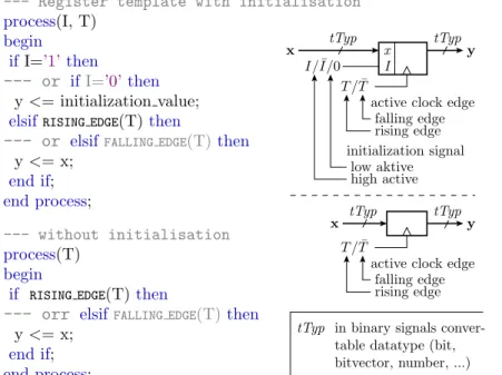
--- Register template with initialisation process(I, T)
begin if I=’1’ then
--- or if I=’0’ then y <= initialization value;
elsif RISING EDGE (T) then
--- or elsif FALLING EDGE (T) then y <= x;
end if;
end process;
--- without initialisation process(T)
begin
if RISING EDGE (T) then
--- orr elsif FALLING EDGE (T) then y <= x;
end if;
end process;
T / ¯ T
active clock edge rising edge falling edge
x y
table datatype (bit, bitvector, number, ...)
tTyp tTyp
tTyp
x I T / ¯ T
active clock edge
initialization signal y x
rising edge falling edge
low aktive high active I/ ¯ I/0
tTyp tTyp
in binary signals conver-
Sample process ⇔ register
given are three sampling processes signal a,b,c,d: STD LOGIC ;
signal K,L,M: STD LOGIC VECTOR (2 downto 0);
no initialization; sampling with the rising edge of a
process(a) begin
if RISING EDGE (a) then K(0) <= d;
K(1) <= K(0);
K(2) <= K(1);
end if;
end process;
Initialization with c = 1; sampling with the falling edge of b
process(b, c) begin
if c=’1’ then L <= ”000”;
elsif FALLING EDGE (b) then
L <= K;
end if;
end process;
Prof. G. Kemnitz·Institute of Informatics, Technical University of Clausthal May 14, 201210/135
Initialization with c = 1; sampling with the raining edge of a
process(a, c) begin
if c=’1’ then
M <= ”010”;
elsif RISING EDGE (a) then
M <= K;
end if;
end process;
inputs, outputs and parameters of the described registers
data input signal d K(0) K(1) K K
data output signal K(0) K(1) K(2) L M
bit width 1 1 1 3 3
clock signal a ↑ a ↑ a ↑ b ↓ a ↑
initialization signal – – – c (H) c (L)
initialization value – – – 000 010
↑ – rising edge; ↓ – falling edge; H – high active; L – low active
Register transfer synthesis
extraction of the terminals and parameters of all described registers
Forwarding the data to circuit generators; generation of the registers
The designer
must stick to the description templates
may summarize all registers withe the same initialization and sampling conditions in one sampling process
Advantage of less processes
less calculation effort for simulation
less time critical transitions between different clocked circuit parts
Prof. G. Kemnitz·Institute of Informatics, Technical University of Clausthal May 14, 201212/135
Combinational circuits
Synthesis description of a combinational circuits
imperative behavioral model of a combinatorial circuit:
if one of the input signal switches, new calculation of the output; no memory
Description template:
process with all input signals in the sensitivity list store interim results in the calculation in variables (not signals!)
no further processing of interim results from previous wake-up dates
in each path of control a value must be assigned to each output signal.
additional simplifications for synthesis: no delay, no check for validity
Prof. G. Kemnitz·Institute of Informatics, Technical University of Clausthal May 14, 201214/135
If synthesis finds a process which complies with all rules:
extract of the control flow
substitute operators by logic gates
produce case distinctions by multiplexers.
Circuits of basic gates
b a &
b a ≥ 1
b a ≥ 1
y y <= a or b
y <= a nor b y
b a =1
b a =1
a
0 1 b
a y
s b
a & y y <= a and b
y y <= a nand b
signal a, b, s, y: tBit ;
y
y y <= a xor b
y <= a xnor b y <= not a
if s=1 then y <= a;
else y <= b;
end if ;
(tBit: BIT , BOOLEAN or STD LOGIC ; BOOLEAN : TRUE 7→ 1, FALSE 7→
0; using STD LOGIC the pseudo values for invalid etc. remains unused)
Prof. G. Kemnitz·Institute of Informatics, Technical University of Clausthal May 14, 201216/135
Description & extraction of gates
signal x: STD LOGIC VECTOR (4 downto 0);
signal y: STD LOGIC VECTOR (1 downto 0);
...
process(x)
variable v: STD LOGIC VECTOR (1 downto 0);
begin
A1: v(0):= x(0) and x(1);
A2: v(1):= v(0) nor x(3);
A3: y(0)<=(v(0) and x(2)) or v(1);
A4: y(1)<=((not x(4)) or x(3)) nand v(1);
end process;
x 2
x 1
x 0
y 1
y 0
v 0
v 1
x 3
x 4
& &
≥ 1
&
≥ 1
A1
A2
A3
≥ 1
A4
From case distinctions to multiplexers
if control flow branches by If or Case instructions output or interim values has to be assign in each branch If-Elsif becomes a multiplexer chain
signal a, b, c, p, q, y: STD LOGIC ; ...
process(a, b, c, p, q) begin
if p=’1’ then y<=a;
elsif q=’1’ then y<=b;
else y<=c;
end if;
end process;
0
1 0
a 1 b c q p
y
instead of Else it is also possible to overwrite a default value (even for signals):
y<=c;
if p=’1’ then y<=a; end if;
Prof. G. Kemnitz·Institute of Informatics, Technical University of Clausthal May 14, 201218/135
Parametrized functional blocks
operators with bit vector operands
⇒ functional blocks with bit sizes as parameters arithmetic operation and compare (>, ≥ etc.)
⇒ additional parameter: number representation select statements with more than two cases
⇒ additional parameters: selection values for each data input
register transfer synthesis:
extraction of functional blocks and its parameters circuit generators:
building the circuits out of basic gates; optional incl.
technology mapping, ...
Select statement ⇒ parametrized multiplexer
signal s: STD LOGIC VECTOR (1 downto 0);
signal x1,x2,x3,x4, y: STD LOGIC VECTOR (3 downto 0);
...
process(s, x1, x2, x3,x4) begin
case s is
when ”00” => y <= x1;
when ”01” => y <= x2;
when ”10” => y <= x3;
when others => y <= x4;
end case;
end process;
00 01
11
10 y
x 1
x 2
x 3
x 4
s 2
4 4 4
4
4
parameters: data bit size and select values last selection value must be others 1
1
On one hand selection values such as
0X
,
XU
are forbidden in synthesis descriptions, on the other hand a case-statement has to take into account the whole range of selection values.
Prof. G. Kemnitz·Institute of Informatics, Technical University of Clausthal May 14, 201220/135
Bit comparators
x
0= 0 x
0x
1x
06 = 0 x
0= 1 x
06 = 1 x
1= x
0x
16 = x
0x
0x
1=1 x
0x
1==
x
0x
0x
0x
00
1 FALSE (0) TRUE (1)
0 1 FALSE (0) TRUE (1) TRUE (1) FALSE (0) FALSE (0) TRUE (1)
1 1 TRUE (1) FALSE (0)
0
0 TRUE (1) FALSE (0) FALSE (0) TRUE (1) TRUE (1) FALSE (0)
branch values in if-statements are generally produced by comparisons
in synthesis the Boolean values false and true are
mapped to the value range { 0, 1 }
Arithmetical operations (+, − , *) and >, ≥ etc.
only defined for number and bit vector types the circuit to be generated depends on the number
representation (natural, whole numbers, floating point, ...) types of bit vectors for number representation in this lecture:
--- for unsignd whole numbers
tUnsigned is array ( NATURAL range <>) of STD LOGIC ; --- for signd whole numbers
tSigned is array ( NATURAL range <>) of STD LOGIC ; defined together with the arithmetical, logical and compare operations in the package Tuc.Numeric Synth
Prof. G. Kemnitz·Institute of Informatics, Technical University of Clausthal May 14, 201222/135
Data flow symbols for compare operators
n n
n n
n n n n n
n n
n
0 else b
a
0 else b
a
0 else b
a
0 else b
a 0 else
b a
/=
<
<=
>
>=
1 if a = b 0 else b ==
a
1 a 6 = b
1 if a < b
1 if a ≤ b
1 if a > b
1 if a ≥ b signal a, b: t[Un]signed(n-1 downto 0);
parameters:
bit size n
data type (signed or unsigned whole numbers) 2
2
Other number types will not be used for synthesis in this lecture.
Addition, subtraction and multiplication
signal a: T[Un]signed(n-1 downto 0);
signal b: T[Un]signed(m-1 downto 0);
constant c: T[Un]signed(m-1 downto 0);
a − c a+c
a+b a−b
max(n, m)
n
− c
nm n
n
+c
max(n, m) max(n, m) mn
∗ c
m n*
n+m n+ma*b
a*c
max(n, m)a−b
a a
a b b a
a b + a
b a
subtractor multiplier
adder
sum and difference have the bit size of the larges operand the bit size of a product is the sum of the bit sizes of the operands
operations not listed here (division, power) are generally realized by an operation sequence
Prof. G. Kemnitz·Institute of Informatics, Technical University of Clausthal May 14, 201224/135
Special calculators with arithmetic operations
signal a, b: tUnsigned(2 downto 0);
signal y: tUnsigned(7 downto 0);
...
process(a, b)
variable v: tUnsigned(6 downto 0);
begin
A1: v:= a * "1010";
A2: y<= (’0’&v) + b;
end process;
a 0
+ 8 y
7 3 8 3
b
∗ 10
size of the product: 3 × 4 ⇒ 7 bit
concatenation of a leading one extends first summand to 8 bits
size of the sum: max(3, 8) ⇒ 8 bit
Circuit with adder, comparator, multiplexer and gates
signal a, b, y: tUnsigned(3 downto 0);
signal e, f: STD LOGIC ; ...
process(a, b, e, f) begin
if (a>"0011") and (e or f) =’1’ then y <= a+b;
else y <= b;
end if;
end process;
4 4
4
+ 4
a b
≥ 1
>
&
e f 0011
1 y 0
Prof. G. Kemnitz·Institute of Informatics, Technical University of Clausthal May 14, 201226/135
One select statement, multiple multiplexers
w2
w1 t1 t2
t1 t1 t1 w2 w1 =>
=>
=>
case when when when end case;
s is w3 w4
t2 t2 t2 w3
else
w4 w3
else
{w1, w2, w3, ...}
s u
sonstt1, t2 – any bit or bitvector type u := a;
u := b;
Mux1
v := c;
v := d;
Mux2 u :=u
else;
a
b d
c
v u
v
sonstv := v
else;
assignment of a default value before the select statement
overwrite the default value for select values assigning a
different value
Describing a truth table by a case statement
signal x: STD LOGIC VECTOR (3 downto 0);
signal y: STD LOGIC ; ...
process(x) begin
case x is
when "1000" | "0100" | "0010" | "0001"
=> y <= ’1’;
when others => y <= ’0’;
end case;
end process;
x 0
x 1
x 2
x 3 y
0 0
0 0 0 0
0 1 1 1 1 0
0 0 0 0
1 1 1 1 0 else
Prof. G. Kemnitz·Institute of Informatics, Technical University of Clausthal May 14, 201228/135
Processing + sampling
Combinatorial circuit and sampling register
Combining combinatorial circuitry with the subsequent register in a sampling process reduces simulation effort; changes in description starting from a pure combinatorial process:
clock instead all input signal in the sensitivity list aligning signal assignments to the active clock edge
optional initialization (in addition initialization signal in the sensitivity list etc.)
process(I, T) if I=active then
y <= initial value;
elsif active clock edge of T then
output calculation of the processing function;
y <= assigning the processing result;
end if;
end process ;
Prof. G. Kemnitz·Institute of Informatics, Technical University of Clausthal May 14, 201230/135
Combinatorial circuit with output register
signal a, b, y: STD LOGIC VECTOR (4 downto 0);
signal T, e, f: STD LOGIC ; ...
process(T) begin
if RISING EDGE (T) then if (a>"0011") and
(e or f) =’1’ then y<= a+b;
else y<=b;
end if;
end if;
end process;
4 4
4
4 4
a + b
≥ 1
>
&
e f
0011 T
combinatorial circuit
sampling register
y 1
0
Output register with conditional sampling
signal x, y: STD LOGIC VECTOR (n-1 downto 0);
signal T, E: STD LOGIC ; ...
process(T) begin
if RISING EDGE (T) then if E=’1’ then
y<=x;
end if;
end if;
end process;
n
n n
n
n n
0 1
T x
E
y
x E
T x
E
y
registers may store values for multiple clocks; describing conditional sampling:
multiplexer between input and actual value register extension by an enable input
Prof. G. Kemnitz·Institute of Informatics, Technical University of Clausthal May 14, 201232/135
Sampled signal may processed further
signal y: tUnsigned(3 downto 0);
signal T, I, V, R: STD LOGIC ; ...
process(T, I) begin
if I=’1’ then y<="0000";
elsif RISING EDGE (T) then if V=’1’ then y<=y+"1";
elsif R=’1’ then y<=y-"1";
end if;
end if;
end process;
4 4 4
4 4
4 0 1 0
1 x
I
y +1
− 1
I T
V R
in combinatorial circuits a feedback of the form
y<=y+”1” is not allowed
Up/down counter with enable input
variable tmp: tUnsigned(3 downto 0);
...
if V=’1’ then tmp:=y+"1";
else
tmp:=y-"1";
end if;
if V=’1’ or R=’1’ then y<=tmp;
end if;
4 4
4
0 4
1 +1
− 1
R I
V ≥ 1
x y
I T E
different descriptions of the same function may synthesised to different circuits
way for optimization
Prof. G. Kemnitz·Institute of Informatics, Technical University of Clausthal May 14, 201234/135
Variables as data storage in sampling processes
signal T, x, y: STD LOGIC ; ...
process(T)
variable z: STD LOGIC VECTOR (2 downto 0);
begin
if RISING EDGE (T) then
y <= z(2); z(2):=z(1);
z(1):=z(0); z(0):=x;
end if;
end process;
z 1 z 2
y T
z 0
x
variables, which are read before assignment in the control
flow, store data for one clock period; behavior of a register
variables are only readable and writable within a process /
can can not be used for terminal signals
Behavior of conditional variable assignments
signal T, a, b, c, y0, y1: STD LOGIC ; ...
process(T)
variable v: STD LOGIC ; begin
if RISING EDGE (T) then A1: y0 <= v xor a;
if b=’1’ then A2: v:= c;
end if;
A3: y1 <= v xor a;
end if;
end process;
0 1 c
T a
b =1
=1
y 0
y 1
A1 und A2 variable v statement variable v
statement A3
A1: v is assigned at least one clock earlier (register output)
A3: v may be assigne in the same clock (register input)
Prof. G. Kemnitz·Institute of Informatics, Technical University of Clausthal May 14, 201236/135
Variables that store data may represent in a synthesized circuit different circuit points.
The description of registers by variables is for that error-prone
should be used deliberately.
Latches
Prof. G. Kemnitz·Institute of Informatics, Technical University of Clausthal May 14, 201238/135
Latches, stage triggered memory element
signal E: STD LOGIC ; signal x, y: tTyp;
...
process(x, E)
variable tE: DELAY LENGTH ; begin
if E=’1’ then
y <= invalid after th, x after td;
end if;
--- check setup condition if RISING EDGE (E) then
tE:= now ;
elsif Falling EDGE (E) and ( NOW -tE<ts or x’ LAST EVENT <ts) then
y <= invalid;
end if;
end process;
t
dt
d> t
s> t
st
ht
hL x E
tTyp E
x tTyp y
01
01 01
tTyp
Vorhaltezeit t
sE Freigabeeingang Verz¨ogerungszeit t
dt
hHaltezeit Bit- oder Bitvek- tortyp
x
E
y
einfachere Schaltung als Register; genutzt zur Aufwandsminimierung
das Freigabesignal ist zeit- und glitch-empfindlich
Die Synthesebeschreibungsschablone ist das stark vereinfachte Simulationsmodell:
ohne Zeitangaben
ohne Kontrolle der Vor- und Nachhaltebedingungen ohne Berechnung der G¨ ultigkeitsfenster
process(x, E) begin
if E=’1’ then y <= x;
end if;
end process;
Auch wenn die Kontrollen fehlen, m¨ ussen die Vor- und Nachhaltebedingungen erf¨ ullt sein.
Prof. G. Kemnitz·Institute of Informatics, Technical University of Clausthal May 14, 201240/135
Die T¨ ucken einer Latch-Schaltung am Beispiel
signal x1, x2, y:
std logic vecto r(n-1 downto 0);
...
process(x1, x2) begin
if x1=x2 then y <= x1;
end if;
end process; t d
t h
L x
E w 3
w 1 w 4
w 2 w 3
0
E
1x 1
x 2
y x 2 ==
x 1
F1 F2
F1: m¨ oglich Invalidierung des gespeicherten Wertes
F2: m¨ oglicher ¨ Ubernahmefehler bei ¨ Ubereinstimmung
Blockspeicher mit Latches
signal E: std logic ;
signal a: std logic vector (1 downto 0);
signal x, s, q, y0, y1, y2, y3, s:
std logic vector (3 downto 0);
...
Dec:process(a) begin
case a is
when "00" => s <= "0001";
when "01" => s <= "0010";
when "10" => s <= "0100";
when others => s <= "1000";
end case;
end process;
E x
E x
E x
E x
y
1y
0y
2y
3q
0q
1q
2q
3&
&
&
&
s
0s
1s
2s
3Dec x
E
00 10 01 11
11
s
0s
1E q
0q
1a a
0 1
0 1 0 1 0 1 0 1
Prof. G. Kemnitz·Institute of Informatics, Technical University of Clausthal May 14, 201242/135
Und:process(s, E) begin
if E=’1’ then q <= s;
else q <= "0000";
end if;
end process;
Latch0:process(x, q(0)) begin
if q(0)=’1’ then y0<=x; end if;
end process;
...
E x
E x
E x
E x
y 1
y 0
y 2
y 3
q 0
q 1
q 2
q 3
&
&
&
&
s 0
s 1
s 2
s 3
Dec x
E a
Latch-Schaltungen sind nur mit einer bestimmten Struktur und Ansteuerung laufzeitrobust
UND-Verkn¨ upfung mit E unmittelbar vor den Freigabeeing¨ angen der Latches
E muss inaktiv sein, wenn die Signale s i invalid sind
laufzeitkritische Teile als vorentworfene Schaltungen
einbinden
Latch zur Variablennachbildung in Abtastprozessen
signal T, a, b, c, y: std logic ; ...
process(T)
variable v: std logic ; begin
if rising edge (T) then if b=’1’ then
v:= c;
end if;
y <= v xor a;
end if;
end process;
=1 y
a x E c b
T 0
1 =1 y
b T a c
bei einem Latch ist der ¨ Ubernahmewert sofort, nicht erst im Folgetakt am Ausgang verf¨ ugbar; erspart Multiplexer b muss mit Latch ein glitch-freies Abtastsignal sein
Prof. G. Kemnitz·Institute of Informatics, Technical University of Clausthal May 14, 201244/135
Constraints
Constraints
Zusatzinformationen f¨ ur die Synthese;
Festlegungen/Empfehlungen f¨ ur
die Struktur und die Technologieabbildung (z.B. keep , um die Wegoptimierung bestimmter Signale und
Teilschaltungen zu verbieten)
die Platzierung (z.B. Zuordnung zwischen Anschlusssignalen und Schaltkreispins)
maximale Verz¨ ogerungszeiten (Taktfrequenz oder -periode, Eingabe-Register-Verz¨ ogerung etc.)
F¨ ur Praktikum (ise/Versuchsboard mit Xilinx-FPGA):
Beschreibung der Pin-Zuordnung und der Taktfrequenz in der ucf-Datei (user constraints file):
<loc> ..
Prof. G. Kemnitz·Institute of Informatics, Technical University of Clausthal May 14, 201246/135
Entwurfsfehler
Entwurfsfehler und Fehlervermeidung
Synthesebeschreibungen haben ihre typischen Entwurfsfehler, darunter auch einige die nur das Zeitverhalten und/oder die Zuverl¨ assigkeit der synthetisierten Schaltung beeintr¨ achtigen und dadurch schwer zu finden sind.
Prof. G. Kemnitz·Institute of Informatics, Technical University of Clausthal May 14, 201248/135
Speicherverhalten in kombinatorischen Prozessen
x
1x
2z y
not z;
not sz; not z;
zb;
not
&
0 1
0 1
0 1
0 1
0 1 0
process
1begin
end process;
(x1);
variable
process begin
end process;
(x1, x2);
sz <= x1 and x2;
process variable begin
end process;
z := x1 and x2;
(x1, x2);
y <=
yF2 <=
z := x1
(x1, x2);
process variable begin
end process;
z := x1 and x2;
and x2;
yF3 <=
yF1 <=
x
2x
1y y
F1y
F2y
F3signal x1, x2, sz, y, yF1, yF2, yF3:
z: z:
z:
Fehlverhalten Soll-Verhalten
F2 F3
F1 korrekt
warte
;
; ;
;
STD LOGIC
STD LOGIC STD LOGIC
STD LOGIC
F1: fehlendes Signal in der Weckliste; F2: Signal statt Variable
als Zwischenspeicher; F3: Variablenwert vor der Zuweisung
ausgewertet
Fallunterscheidung mit fehlender Zuweisung
signal x1, x2, x3 y: std logic vector (3 downto 0);
signal s: std logic vector (1 downto 0);
...
process(s, x1, x2, x3) begin
case s is
when "00" => y <= x1;
when "01" => y <= x2;
when "10" => y <= x3;
when others => null;
--- Korrektur: y <= x3 statt null end case;
end process;
4 4
4 4
4 4 4
4
00 x
101 sonst x
3x
2y
s 2
&
s
y L x E 00
x
101 10 x
3x
22
auch wenn ein Auswahlwert nicht auftreten kann, ist in einer Multiplexerbeschreibung ein Wert zuzuweisen
Prof. G. Kemnitz·Institute of Informatics, Technical University of Clausthal May 14, 201250/135
Fehlersymptome:
nicht synthetisierbar oder unerwarteter Latch-Einbau Fehlervermeidung
Verwendung der Kurzform nebenl¨ aufige Signalzuweisung , im Beispiel aus UND und Inverter:
y <= not (x1 and x2);
sp¨ ater f¨ ur beliebig komplexe kombinatorische Schaltungen:
signal x: tEingabe;
signal y: tAusgabe;
function f(x: tEingabe) return tAusgabe;
...
y <= invalid after th, f(x), after td ; Synthesebeschreibung ohne grau unterlegte Teile
nebenl¨ aufige Signalzuweisungen und Funktionen k¨ onnen kein
Speicherverhalten beschreiben / keinen der skizzierten
Fehler enthalten
B¨ osartige Timing-Probleme
Symptome:
zul¨ assige Taktfrequenz laut Synthsereport zu niedrig messbare Zeitprobleme an den Anschlusssignalen Anderung der Beschreibung zeigt keine Wirkung ¨
Fehlerwirkung nicht mit Simulation nachstellbar / nicht reproduzierbar
Ursache sind in der Regel fehlende oder falsche Zeit-Constraints Constraint-Doku lesen und Constraints richtig beschreiben
Prof. G. Kemnitz·Institute of Informatics, Technical University of Clausthal May 14, 201252/135
Gutartige Timing-Probleme
Symptome:
Zusatzverz¨ ogerungen um ganze Taktperioden Fehlerwirkung mit Simulation nachstellbar typische Ursachen
Zwischenergebnisse in Abtastprozessen in Signalen statt Variablen weitergereicht
Variablenwerte vor der Wertzuweisung ausgewertet
Denkfehler im Algorithmus und in der Ablaufplanung
Nicht synthetisierbar
ungeeignete Funktion, z.B. kein gerichteter Berechnungsfluss
x
2x
30 1
1 0 0 0
setzen speichern
y r¨ ucksetzen
2 · t
dt t
dGesamtschaltung x
1= 0 x
1= 1, x
2= x
3= 0
0
y
1G1 G2 G3 y
≥ 1 G1
=1
≥ 1
≥ 1
≥ 1
G2 G3
x
1y x
2x
3G2 G3
x
2x
3a)
b)
c) y
Speicher- oder Schwingungsverhalten bei der Simulation ungeeignete Beschreibungsstruktur
Wenn das simulierte Verhalten ok. ist, ausweichen auf bew¨ ahrte Beschreibungsschablonen (Doku des
Syntheseprogramms lesen)
Prof. G. Kemnitz·Institute of Informatics, Technical University of Clausthal May 14, 201254/135
Zusammenfassungf
Zusammenfassung
Eine Synthesebeschreibung ist ein vereinfachtes
Simulationsmodell ohne Verz¨ ogerungen und ohne Berechnung der Signalg¨ ultigkeit etc.. Zuordnungen:
Signalzuweisung bei aktiver Taktflanke ⇒ Register
logische, arithmetische und Vergleichsoperatoren ⇒ Gatter, Rechenwerke und Komparatoren
Fallunterscheidungen und Auswahlanweisungen ⇒ Multiplexer
zustandsgesteuerte bedingte Zuweisungen ⇒ Latches, laufzeitempfindlich
Zeit- und Strukturanforderungen werden durch Constraints beschrieben. Bei einer Synthesebeschreibung kommt es nicht nur auf die Funktion, sondern auch auf die Beschr¨ ankung auf
bew¨ ahrte Beschreibungsschablonen an.
Prof. G. Kemnitz·Institute of Informatics, Technical University of Clausthal May 14, 201256/135
Aufgaben
Aufgabe 2.1: Registerextraktion
signal K,L,M,N,P,Q: std logic vector (7 downto 0);
signal c: std logic vector (1 downto 0);
process(c(0)) begin
if rising edge (c(0)) then L <= K;
end if;
end process;
process(c(1)) begin
if rising edge (c(1)) then N<=M; M<=L;
end if;
end process;
process(c(1)) begin
if falling edge (c(1)) then P<=L; Q<=P;
end if;
end process;
Anschlusssignale, Ubernahmebedingungen ¨ etc. aller beschriebenen Register suchen
Signalflussplan zeichnen
Prof. G. Kemnitz·Institute of Informatics, Technical University of Clausthal May 14, 201258/135
Aufgabe 2.2: Beschreibung als synthesef¨ ahiger kombinatorischer Prozess
0 1
0
1 +
≥ 1
&
0
1 y
s 1 4 4
tUnsigned(3 downto 0)
STD LOGIC
4 4 4 4 4
a b s 0
4 4
4
4
Aufgabe 2.3: Beschreibung als synthesef¨ ahiger Abtastprozess
signal y: tSigned(7 downto 0);
signal R, E, I, T: std logic ;
+1
− 1 0 1
0
1 x y
I 8
8
8 8 8
R E I T ¯
Initialisierungswert alles null
Prof. G. Kemnitz·Institute of Informatics, Technical University of Clausthal May 14, 201260/135
Aufgabe 2.4: Synthesef¨ ahige Beschreibung mit m¨ oglichst wenig Prozessen
signal T, I, x, x del, y: std logic ;
I x I x’
Reg2 Reg1 G
==
T
x y
Initialwert 0
Aufgabe 2.5: Synthesef¨ ahige Beschreibung des Automaten
01 00 10 11
00 01 10 11
00 01 10 11
00 01 10 11 00 01 10
00 01 10 11
00 01 10 11
00 01 10 11 00 01 10 d)
s x :
s + = f s (x, s) y
x x
I s + s 2
2 2
y = f a (x, s) f a (x, s)
I T f s (x, s)
Prof. G. Kemnitz·Institute of Informatics, Technical University of Clausthal May 14, 201262/135
Aufgabe 2.6: Extraktion des Signalflussplans
signal x, tmp, acc, y: std logic vector (3 downto 0);
signal op: std logic vector (1 downto 0);
signal T: std logic ; ...
process(T) begin
if rising edge (T) then case op is
when "00" => acc <= x;
when "01" => acc <= acc + tmp;
when "10" => acc <= acc - tmp;
when others => null;
end case;
end if;
tmp <= x;
end process;
y <= acc;
Logikoptimierung
Prof. G. Kemnitz·Institute of Informatics, Technical University of Clausthal May 14, 201264/135
Definition 1
Eine n-stellige logische Funktion ist eine Abbildung eines n-Bit-Vektors aus freien bin¨ aren Variablen auf eine abh¨ angige bin¨ are Variable:
f : B n → B mit B = { 0, 1 } bzw.
y = f (x n−1 , x n−2 , . . . , x 0 ) mit y, x i ∈ { 0, 1 } (y – abh¨ angige Variable; x i freie Variablen).
Jede logische Funktion kann durch praktisch unbegrenzt viele logische Ausdr¨ ucke und Schaltungen nachgebildet werden.
Die Register-Transfer-Synthese extrahiert logische Funktionen in Form von kombinatorischen
Teilschaltungsbeschreibungen.
Anschließende Vereinfachung:
Vereinfachung logischer Ausdr¨ ucke mit Hilfe der Schaltalgebra (dieser Abschnitt)
Darstellung der logischen Ausdr¨ ucke zur Vereinfachung als bin¨ are Entscheidungsdiagramme (n¨achster Abschnitt).
Bereits behandelte Vereinfachungstechniken:
Konstantenelimination
beseitigt alle Operationen, bei denen freie Variablen mit konstanten Werten belegt sind; reduziert die Stelligkeit und die Anzahl der Operationen
Verschmelzung
fasst gleiche Berechnungsschritte mit gleichen Operanden zusammen und reduziert so die Anzahl der Operationen
Prof. G. Kemnitz·Institute of Informatics, Technical University of Clausthal May 14, 201266/135
Umformungsregeln
Umformungsregeln f¨ ur logische Ausdr¨ ucke
Umformungsregel Bezeichnung
¯ ¯
x = x doppelte Negation x ∨ 1 = 1
x ∨ x ¯ = 1 x ∧ 0 = 0 x ∧ x ¯ = 0
Eliminationsgesetze
x 1 ∨ (x 1 ∧ x 2 ) = x 1 x 1 ∧ (x 1 ∨ x 2 ) = x 1
Absorbtionsgesetze
¯
x 1 ∨ x ¯ 2 = x 1 ∧ x 2
¯
x 1 ∧ x ¯ 2 = x 1 ∨ x 2
de morgansche Regeln
Prof. G. Kemnitz·Institute of Informatics, Technical University of Clausthal May 14, 201268/135
Umformungsregel Bezeichnung x 1 ∧ x 2 = x 2 ∧ x 1
x 1 ∨ x 2 = x 2 ∨ x 1
Kommutativgesetze (x 1 ∨ x 2 ) ∨ x 3 =
x 1 ∨ (x 2 ∨ x 3 ) (x 1 ∧ x 2 ) ∧ x 3 =
x 1 ∧ (x 2 ∧ x 3 )
Assoziativgesetze
x 1 ∧ (x 2 ∨ x 3 ) = (x 1 ∧ x 2 ) ∨ (x 1 ∧ x 3 )
x 1 ∨ (x 2 ∧ x 3 ) = (x 1 ∨ x 2 ) ∧ (x 1 ∨ x 3 )
Distributivgesetze
Beweis der Umformungsregeln
Aufstellen und Vergleich der Wertetabellen.
F¨ ur die de morganschen Regeln gilt z.B.:
x 1 x 2 x ¯ 1 ∨ x ¯ 2 x 1 ∧ x 2 x ¯ 1 ∧ x ¯ 2 x 1 ∨ x 2
0 0 1 1 1 1
0 1 1 1 0 0
1 0 1 1 0 0
1 1 0 0 0 0
Prof. G. Kemnitz·Institute of Informatics, Technical University of Clausthal May 14, 201270/135
Anwendung der Umformungsregeln zur Schaltungsvereinfachung
mehrfache Negationen im Signalfluss heben sich paarweise auf
z = x 1 ∧ x 2 ∧ x 3
y = ¯ z
&
x 1
x 2
x 3
&
x 1
x 2
x 3
y z y
y = x 1 ∧ x 2 ∧ x 3
= x 1 ∧ x 2 ∧ x 3
doppelte Anwendung der Eliminationsgesetze
& 1 y
y = (x 1 ∧ x ¯ 1
| {z }
0
) ∧ x 2 = 0 ∧ x 2
| {z }
0
= 0 = 1 x 2
x 1 y
Prof. G. Kemnitz·Institute of Informatics, Technical University of Clausthal May 14, 201272/135
Anwendung des Absorbtionsgesetzes
&
&
≥ 1
&
x 1
x 2 y
Assoziativgesetz:
Absorbtionsgesetz:
gegeben Funktion: y = (x 1 ∧ x 2 ) ∧ (x 2 ∨ x 3 ) y = x 1 ∧ (x 2 ∧ (x 2 ∨ x 3 )) y = x 1 ∧ x 2
x 1
x 2
x 3
y
Suchproblem: in gegebenen Ausdr¨ ucken
Anwendungsm¨ oglichkeiten f¨ ur die Gesetze finden
Terme nutzen die Grundoperationen UND, ODER und Negation
technische Gatter haben oft eine invertierte Ausgabe (siehe sp¨ ater Konstruktion von Logikgattern aus Transistoren ) Umformung der UND-ODER-Form in die
NAND-NAND-Form x 1
x 2
x 3
x 4
&
≥ 1
&
x 1
x 2
x 3
x 4
&
&
&
y y
y = (x 1 ∧ x 2 ) ∨ (x 3 ∧ x 4 ) y = (x 1 ∧ x 2 ) ∨ (x 3 ∧ x 4 ) y = x 1 ∧ x 2 ∧ x 3 ∧ x 4
de morgansche Regel:
doppelte Negation:
gegebene Funktion:
Prof. G. Kemnitz·Institute of Informatics, Technical University of Clausthal May 14, 201274/135
Umformung der ODER-UND-Form in die NOR-NOR-Form
≥ 1
≥ 1
&
x 1
x 2
x 3
x 4
x 1
x 2
x 3
x 4 ≥ 1
≥ 1
≥ 1
y y
y = (x 1 ∨ x 2 ) ∧ (x 3 ∨ x 4 ) y = (x 1 ∨ x 2 ) ∧ (x 3 ∨ x 4 ) y = x 1 ∨ x 2 ∨ x 3 ∨ x 4
gegebene Funktion:
doppelte Negation:
de morgansche Regel:
Optimierungsziele
Prof. G. Kemnitz·Institute of Informatics, Technical University of Clausthal May 14, 201276/135
Optimierungsziele
minimale Gatteranzahl minimale Chipfl¨ ache
minimaler Stromverbrauch minimale Verz¨ ogerung etc.
Regel zur Geschwindigkeitsoptimierung: B¨ aume statt Ketten
Pfad der l¨ angsten Verz¨ogerung t
dOpt
dOpt
dOpt
dOpt
dOpt
dOpt
dOpt
dOpt
dOpx
0x
1x
2x
3x
4x
5x
6y y
x
0x
1x
6x
5x
4x
3x
2t
dKette= n · t
dOpt
dBaum≥ log
2(n) · t
dOpb) a)
◦ assoziative Operation (Zusammenfassungsreihenfolge vertauschbar)
oft unterscheiden sich die L¨ osungen f¨ ur minimalen Aufwand und max. Geschwindigkeit etc.
l¨ angster Pfad
=1
=1
=1
y
2y
1y
0x
3x
2x
1x
0a)
=1
=1
=1 =1 x
2x
1x
0x
3y
0y
1y
2c) b) te L¨osungen
Verz¨ogerung minimale
minimaler Aufwand
Aufwand andere optimier- max
min
min max
Signalverz¨ogerung
Prof. G. Kemnitz·Institute of Informatics, Technical University of Clausthal May 14, 201278/135
Konjunktionsmengen
Logikminimierung mit Konjunktionsmengen
klassische Verfahren
KV-Diagramm: graphisches Verfahren
Quine-McCluskey: gleicher Algorithmus als Suchproblem Konjunktion: Term, der direkte oder invertierte
Eingabevariablen UND-verkn¨ upft, z.B.:
x 3 ∧ x ¯ 2 ∧ x 1 ∧ x ¯ 0 = x 3 x ¯ 2 x 1 x ¯ 0 (K 1010 )
| {z }
verk¨ urzte Schreibweisen
Minterm: Konjunktion, die alle Eingabevariablen entweder in direkter oder in negierter Form enth¨ alt.
Satz: Jede logische Funktion l¨ asst sich durch eine Menge von Konjunktionen darstellen, die ODER-verkn¨ upft werden.
Prof. G. Kemnitz·Institute of Informatics, Technical University of Clausthal May 14, 201280/135
Beweis: Jede logische Funktion l¨ asst sich durch eine Wertetabelle darstellen. Jeder Zeile einer
Wertetabelle ist ein Minterm zugeordnet, der genau dann Eins ist, wenn die Zeile ausgew¨ ahlt ist.
Die Funktion ist entweder die
ODER-Verkn¨ upfung der Minterme, f¨ ur die y = 1 ist x n − 1 x 2 x 1 x 0
· · ·
(programmierbar) ODER-Matrix
y 0 y 1 y 2 y m − 1
· · · (1 aus 2 n - Decoder)
UND-Matrix
2 n vollst¨ andige Konjunk- tionen (Produktterme)
· · ·
negierte ODER-Verkn¨ upfung der Minterme, f¨ ur die y = 0 ist.
x 2 x 1 x 0 Konjunktion y x 2 x 1 x 0 Konjunktion y 0 0 0 x ¯ 2 x ¯ 1 x ¯ 0 (K 000 ) 0 1 0 0 x 2 x ¯ 1 x ¯ 0 (K 100 ) 1 0 0 1 x ¯ 2 x ¯ 1 x 0 (K 001 ) 1 1 0 1 x 2 x ¯ 1 x 0 (K 101 ) 1 0 1 0 x ¯ 2 x 1 x ¯ 0 (K 010 ) 0 1 1 0 x 2 x 1 x ¯ 0 (K 110 ) 1 0 1 1 x ¯ 2 x 1 x 0 (K 011 ) 0 1 1 1 x 2 x 1 x 0 (K 111 ) 0
Entwicklung nach den Einsen: { K 001 , K 100 , K 101 , K 110 } ⇒ y = ¯ x 2 x ¯ 1 x 0 ∨ x 2 x ¯ 1 x ¯ 0 ∨ x 2 x ¯ 1 x 0 ∨ x 2 x 1 x ¯ 0
Entwicklung nach den Nullen: { K 000 , K 010 , K 011 , K 111 } ⇒ y = ¯ x 2 x ¯ 1 x ¯ 0 ∨ x ¯ 2 x 1 x ¯ 0 ∨ x ¯ 2 x 1 x 0 ∨ x 2 x 1 x 0
= ¯ x 2 x ¯ 1 x ¯ 0 ∧ x ¯ 2 x 1 x ¯ 0 ∧ x ¯ 2 x 1 x 0 ∧ x 2 x 1 x 0
= (x 2 ∨ x 1 ∨ x 0 ) (x 2 ∨ x ¯ 1 ∨ x 0 ) (x 2 ∨ x ¯ 1 ∨ x ¯ 0 ) (¯ x 2 ∨ x ¯ 1 ∨ x ¯ 0 )
Prof. G. Kemnitz·Institute of Informatics, Technical University of Clausthal May 14, 201282/135
Vereinfachungsgrundlage
Satz: Zwei Konjunktionen, die sich nur in der
Invertierung einer Variablen unterscheiden, k¨ onnen zu einer Konjunktion mit einer Variablen weniger zusammengefasst werden.
Schritt ODER-Verkn¨ upfung Konjunktionsmenge 1 . . . ∨ x 2 x ¯ 1 x ¯ 0 ∨ x 2 x ¯ 1 x 0 ∨ . . . { . . . , K 100 , K 101 , . . . } 2 . . . ∨ x 2 x ¯ 1 (¯ x 0 ∨ x 0 ) ∨ . . .
3 . . . ∨ x 2 x ¯ 1 ∨ . . . { . . . , K 10∗ , . . . } nur Abweichung in Stelle Eins
Wert von x 1 don’t care , in VHDL ’-’
eine Konjunktion weniger
KV-Diagramme
Prof. G. Kemnitz·Institute of Informatics, Technical University of Clausthal May 14, 201284/135
Aufbau eines KV-Diagramms
KV Karnaugh und Veitch
K 0010
K 0011
K 0001
K 0000 K 0100
K 0101
K 0111
K 0110
K 1100
K 1101
K 1111
K 1000
K 1001
K 1010
K 1011
K 1110
22 2 2
2 2 2 2
3 3 3 3
3 3 3 3
3 3 3 3
0 0 0 0
0 0 0 0
1 1 1 1
1 1 1 1
1 1 1 1
x 0
x 1
x 3
x 2
Tafel entwickeln von hieraus an der
Tabellarische Anordnung der Funktionswerte so, dass sich
die Konjunktionen der benachbarten Stellen genau in einer
Negation unterscheiden.
Zusammenfassen der ausgew¨ ahlten Konjunktionen zu Bl¨ ocken der Kantenl¨ ange eins, zwei oder vier:
K 000 -
K - 11 -
K 10 -- K - 10 -
y = 0 y = 1 K 0010
K 0011
K 0001
K 0000 K 0100
K 0101
K 0111
K 0110
K 1100
K 1101
K 1111
K 1000
K 1001
K 1010
K 1011
K 1110
K 001 -
2 2 2 2
2 2 2 2
3 3 3 3
3 3 3 3
3 3 3 3
0 0 0 0
0 0 0 0
1 1 1 1
1 1 1 1
1 1 1 1
x 0
x 1
x 3
x 2
Minimierte Konjunktionsmenge der Einsen
{ K 000- , K -11- , K 10-- } ⇒ y = ¯ x 3 x ¯ 2 x ¯ 1 ∨ x 2 x 1 ∨ x 3 x ¯ 2 Minimierte Konjunktionsmenge der Nullen:
{ K 001- , K -10- } ⇒ y = ¯ x 3 x ¯ 2 x 1 ∨ x 2 x ¯ 1
Prof. G. Kemnitz·Institute of Informatics, Technical University of Clausthal May 14, 201286/135
Praktische Arbeit mit KV-Diagrammen
Geordnete Tabelle mit Funktionswerten
Optimierungsziel: m¨ oglichst große und m¨ oglichst wenige Bl¨ ocke
Bl¨ ocke d¨ urfen sich ¨ uberlagern
x 0
x 1
x 2
x 3
0
1 1 1
1 1
1
0 0
0 0 0 0
0
0 0
d b c
d
a
a: ¯ x 3 x ¯ 1 x 0
b: x 2 ¯ x 1 x 0
c: ¯ x 3 x 2 x 0
y = ¯ x 3 x ¯ 1 x 0 ∨ x 3 ¯ x 1 x 0 ∨ x ¯ 3 x 2 x 0 ∨ x 3 x 2 x ¯ 0
d: x 3 x 2 x ¯ 0
zirkulare Blockbildung ¨ uber den Rand hinaus und die Entwicklung nach den Nullen sind auch zul¨ assig
x 0
x 2
x 3
0
1 1 1
1 1
1
0 0
0 0 0 0
0
0 0
x 1
de a
c a c a
a
b a
c a
b
b b
a c
a
y = ¯ x 2 x ¯ 0 ∨ x ¯ 2 x 1 ∨ x ¯ 3 x ¯ 0 ∨ x 3 x ¯ 2 ∨ x 3 x 1 x 0
a: ¯ x 2 x ¯ 0
b: ¯ x 2 x 1
c: ¯ x 3 x ¯ 0
d: x 3 x ¯ 2
e: x 3 x 1 x 0
Prof. G. Kemnitz·Institute of Informatics, Technical University of Clausthal May 14, 201288/135
KV-Diagramme mit don’t-care-Feldern
don’t-care-Felder kennzeichnen Eingabem¨ oglichkeiten, die im normalen Betrieb nicht auftreten
ihr Wert wird so festgelegt, dass sich m¨ oglichst wenige und m¨ oglichst große Bl¨ ocke bilden lassen
x 2
x 1
x 3
x 0
1 1
0
0 0
0
1 1 -
- - - 0
1
1 1
b c
d a
e
d
a: ¯ x 1 ¯ x 0
b: x 2 x 1 x 0
c: x 3 x 1 x 0
d: ¯ x 3 x ¯ 2 x ¯ 0
e: ¯ x 3 x ¯ 2 x ¯ 1
y = ¯ x 1 x ¯ 0 ∨ x 2 x 1 x 0 ∨ x 3 x 1 x 0
∨ x ¯ 3 x ¯ 2 x ¯ 0 ∨ x ¯ 3 x ¯ 2 x ¯ 1
KV-Diagramme f¨ ur zwei- und dreistellige Funktionen
Verringerung der Anzahl der Nachbarfelder, die sich in einer Negation unterscheiden auf drei bzw. zwei
Halbierung der H¨ ohe und/oder der Breite
K 001
K 000 K 010
K 011
K 110
K 111
K 100
K 101
K 010
K 011
K 001
K 000 K 100
K 101
K 111
K 110
K 01
K 10
K 11
K 00
0 0 0 0
0 0
0 0 2 2 2 2
0 0
1 1
2 2 2
2 2 2
1 1
1 1
1 1 1
1 1 1
x 0
x 1
x 0
x 1
x 2
x 0
x 1
x 2
Prof. G. Kemnitz·Institute of Informatics, Technical University of Clausthal May 14, 201290/135
KV-Diagramme f¨ ur sechsstellige Funktionen
x
0x
1x
2x
3x
0x
1x
0x
1x
2x
3x
2x
30 1 1
1 0 0 0 0
0 1
1 1
0 0
0 1 0
1 1 1 0
0 0 0
0 1
1 1
0 0
0 1
0 1 1
0 0
0 1 1
0 0
0 1 0
0 1
1 0
1 1
0 0
0 0 0
0 1 0 0 0 0
1 1 0
1 1 1 0
0 0 0
0 1
0 0
0 1 0
0 x
4x
5x
4= 0 x
4= 1
x
5= 0
x
5= 1
b c
d a
b
d a
b
c
d d
c
d a
d a
a: ¯ x
5x
2¯ x
1b: ¯ x
4x ¯
3x ¯
2x
1c: x
5x
3x ¯
1d: x
3x ¯
2x
1x ¯
0y = ¯ x
5x
2x ¯
1∨ x ¯
4x ¯
3x ¯
2x
1∨ x
5x
3¯ x
1∨ x
3x ¯
2x
1x ¯
0Schaltungen mit mehreren Ausg¨ angen
x y
x
0x
0x
1x
1x
2x
2x
2x
2x
3x
3x
3x
3y
0y
2y
4y
6y
3y
1y
50000 0001 0010 0011 0100 0101 0110 0111 1000 1001 belie- sonst
big
0 0 1
1 1 1 1 1
1 - 1 - - -
- -
0 0
0 1
1 1
1 1
1 1 - - - -
- - 0
1 1 1 1
1
1 1
1
1 - - - -
- - 1
1 1 1
1
1 1
1 0
0 - - - -
- -
0 0
0 1 1 1
1
1 1
1 - - - -
- -
. . . 1
1 0
0 0
0 0
- - - -
- - 1
0
1
0
0 0 0 1 1 1
1 1 - 1 - - -
- -
y
0y
1y
2y
3y
4y
5y
6a := ¯ x
3x ¯
2x ¯
1x
0b := x
2¯ x
1x ¯
0c := x
2¯ x
1x
0d := x
2x
1x ¯
0e := ¯ x
2x
1x ¯
0 ab
a b
f e
c
d
j f b
a
h
i g
Prof. G. Kemnitz·Institute of Informatics, Technical University of Clausthal May 14, 201292/135
signal x: std logic vector (3 downto 0);
signal y: std logic vector (6 downto 0);
...
process(x)
variable a,b,c,d,e,f,g,h,i,j: std logic ; begin
a := not x(3) and not x(2) and not x(1) and x(0);
b := x(2) and not x(1) and not x(0);
c := x(2) and not x(1) and x(0);
d := x(2) and x(1) and not x(0);
e := not x(2) and x(1) and not x(0);
...
y(0)<=not(a or b);
y(1)<=not(c or d);
y(2)<=not e;
...
end process;
x
3x
3x
3x
0x
2x
2x
2x
10 0 1
1 1 1 1 1
1 - 1 - - -
-
- 0
1 1 1 1
1
1 1
1
1 - - - -
- - 1
1 1 1
1
1 1
1 0
0 - - - -
- -
y
0y
1y
2a b
e c
d
Beispiel f¨ ur einen Automatenentwurf
R/N
A B
C D
V/L
R/L V/K
R/K
V/M R/M
H/N V/N H/M
H/L H/K
00(A) 01(B) 10(C) 11(D) 01(H) 00(V)
00(A) 01(B) 10(C) 11(D)
01(H) 00(K) 01(L) 10(M) 11(N) 00(V) 01(L) 10(M) 11(N) 00(K)
10(R) 11(N) 00(K) 01(L) 10(M) V, A, K
Symbol H, B, L R, C, M D, N
s, s
+y Zustand, Folgezustand (je 2 Bit) Eingabesignal (2 Bit)
x
Ausgabesignal
a) b)
c)
10(R) 11(D) 00(A) 01(B) 10(C) s
+= f
s(x, s)
01(B) 00(A) 10(C) 11(D) s x
00
Code 01 10 11
symbolische Eingabewerte symbolische Zust¨ ande V, H, R
A, B, C, D
symbolische Ausgabewerte K, L, M, N
y = f
a(x, s)
Zustandscodierung ist so gew¨ ahlt, dass y = s + gilt
Prof. G. Kemnitz·Institute of Informatics, Technical University of Clausthal May 14, 201294/135
Aufstellen der KV-Diagramme
s
1s
1x
1x
0s
0s
00 1
0
1 0 1
0 1
- - - -
1
1 1 0
0
1 0 1
0
- - - -
1 0 0 1
s
+0= y
0s
+1= y
10 V
H
R -
A B D C A B D C
0 1
a a
b a a
a
d c
b e