Characterization of hybrid solar cells prepared from poly-thiophenes and silicon
Dissertation
zur Erlangung des akademischen Grades
doctor rerum naturalium
(Dr. rer. nat.)
im Fach Physik eingereicht an der
Mathematisch-Naturwissenschaftlichen Fakultät der Humboldt-Universität zu Berlin
von
Dipl.-Ing. Matthias Karl Ludwig Zellmeier
Präsident der Humboldt-Universität zu Berlin Prof. Dr. Jan-Hendrik Olbertz
Dekan der Mathematisch-Naturwissenschaftlichen Fakultät Prof. Dr. Elmar Kulke
Gutachter: 1. Prof. Dr. Norbert Koch 2. Prof. Dr. Norbert H. Nickel 3. Prof. Dr. Norbert Esser Tag der mündlichen Prüfung: 04.11.2016
Abstract
Abstract
The scope of this thesis was the development of a hybrid solar cell based on silicon in which the inorganic semiconductor, the organic polymer and the contact system are combined in such a manner to result in a photovoltaic device with high power conversion efficiency. To reach this goal several measures were taken. New polymer materials derived from the prototypical organic semiconductor poly(3-hexylthiophene-2,5-diyl) (P3HT), namely poly(3-[3,6- dioxaheptyl]-thiophene) (P3DOT) and poly(3-[2,5,8-trioxanonyl]-thiophene) (P3TOT), were extensively characterized regarding its structural properties.
Poly-thiophene/c-Si hybrid solar cells fabricated from these new polymers exhibited power conversion efficiencies up to 11 %.
The energy level alignment of these poly-thiophene/c-Si hybrid interfaces was studied using photoelectron spectroscopy. Furthermore, the influence of the contact system on the underlying wafer is investigated with surface photovoltage measurements. The measurements revealed the formation of an inversion layer beneath the silicon surface due to the semitransparent metal contact used in the devices. Therefore, these devices can be classified as MIS inversion layer solar cells.
To further improve the hybrid poly-thiophene/c-Si solar cells by substituting the semitransparent metal contact, graphene was implemented in the device design as a transparent front contact. The carbon monolayer only absorbs 2.7 % of the incident light and has excellent electronic properties. The CVD grown graphene sheet had a lateral size of up to 1 cm2 and was applied onto the solar cell using a non-destructive and water-free transfer process. However, despite the successful transfer the power conversion efficiency was restricted by the low fill factor due to a low charge carrier density in the graphene. A calculation based on the electrical losses indicated that the problem could be overcome by a combination of multilayer graphene and an additional metal grid structure to increase conductivity.
As a last step, hybrid solar cells in the combination P3HT/polycrystalline silicon absorbers on glass were fabricated for the first time. The inverted device structure used for these solar cells proved beneficial for the lifetime. These devices were stable for up to 3 months without additional encapsulation.
Kurzzusammenfassung
Kurzzusammenfassung
Das Hauptaugenmerk dieser Arbeit liegt auf der Entwicklung einer Hybridsolarzelle, in der der anorganische Halbleiter Silizium, das organische Polymer und das Kontaktsystem so aufeinander abgestimmt sind, dass ihre Kombination zu einem Bauelement mit hohem Wirkungsgrad führt. Um dieses Ziel zu erreichen wurden verschiedene Maßnahmen ergriffen. Neue Polymermaterialien, abgeleitet von dem prototypischen organischen Halbleiter poly(3-hexylthiophen-2,5-diyl) (P3HT), namentlich poly(3-[3,6-dioxaheptyl]- thiophen) (P3DOT) und poly(3-[2,5,8-trioxanonyl]-thiophen) (P3TOT), wurden umfassend hinsichtlich ihrer Struktur untersucht. Poly-thiophen/c-Si hybride Solarzellen, hergestellt aus diesen neuen Polymeren, erreichten Effizienzen bis zu 11 %.
Die vollständigen Banddiagramme dieser Poly-thiophen/c-Si Hybridgrenzflächen wurden mittels Photoelektronenspektroskopie aufgenommen.
Außerdem wurde der Einfluss des Kontaktsystems auf die darunter liegenden Schichten mittels Oberflächenspannungsspektroskopie untersucht. Das Resultat dieser Messungen weißt eine Inversionslage unter der Siliziumoberfläche nach, die sich aufgrund des verwendeten semitransparenten Metallkontaktes formt.
Dadurch lassen sich diese Bauteile als MIS-Inversionsschicht-Solarzelle kategorisieren.
Um die Hybridsolarzellen weiter zu verbessern, wurde versucht den semitransparenten Metallkontakt durch Graphen zu ersetzen. Diese Kohlenstoffmonolage besticht durch eine geringe Absorption von nur 2,7 % bei herausragenden elektronischen Eigenschaften. Das Graphen wurde durch einen CVD-Prozess gewachsen und erreichte eine laterale Ausdehnung von bis zu 1 cm2. Der Übertrag auf die Solarzelle erfolgte mittels eines Wasser- und Zerstörungsfreiem Transferprozess. Trotz dem erfolgreichen Aufbringen des Graphen limitierte ein geringer Füllfaktor aufgrund der geringen Ladungsträgerdichte im Graphen den Wirkungsgrad der Solarzelle. Eine Berechnung der elektrischen Verluste weist darauf hin, dass eine Kombination aus mehrlagigem Graphen und zusätzlichem Metallkontaktgitter Abhilfe schaffen kann.
In einem letzten Schritt wurde das Polymer P3HT zum ersten Mal mit polykristallinen Siliziumabsorbern auf Glas kombiniert. Die invertierte Zellstruktur, die hierbei zu Anwendung kam, erwies sich als Vorteilhaft für die Lebensdauer der Solarzelle. Diese waren ohne zusätzliche Verkapselung 3 Monate stabil.
Table of contents
6
Table of contents
1. Introduction ... 8
1.1 Why hybrid solar cells? ... 8
1.2 Scope of the thesis ... 9
2. Fundamentals ... 11
2.1 Inorganic semiconductors ... 12
2.1.1 Silicon ... 13
2.1.2 Crystal structure... 13
2.1.3 Electronic structure ... 15
2.1.4 Comparison of organic and inorganic semiconductors ... 16
2.2 Organic semiconductors ... 18
2.2.1 Bonding forces in organic semiconductors ... 19
2.2.2 Polythiophene semiconductors ... 22
2.2.3 Self-assembled microcrystalline polyalkylthiophenes ... 22
2.2.4 The crystalline structure of poly(3-alkythiophene) ... 23
2.2.5 Absorption of visible light in linear -stacked polyalkylthiophenes ... 25
2.3 Current-voltage characteristics and solar cell parameters ... 30
2.4 The a-Si:H/c-Si heterojunction – a brief introduction ... 33
3. Experimental methods ... 37
3.1 Surface photovoltage measurements ... 38
3.2 X-ray diffraction spectroscopy ... 39
3.3 Photoelectron spectroscopy ... 40
3.4 Charge carrier lifetime measurements ... 42
3.5 Fourier-transform infrared spectroscopy ... 43
4. Sample preparation and device geometry ... 45
4.1 c-Si cleaning and surface conditioning ... 46
4.2 a-Si deposition and back surface field ... 47
4.3 Spin coating of polymer materials ... 50
4.3.1 Influence of the substrate... 50
4.4 Metal deposition ... 51
4.5 Basic device structure and first cell results ... 52
Table of contents
7
5. Side chain engineering of poly-thiophene and its impact on hybrid
solar cells ... 55
5.1 Materials and synthesis ... 56
5.2 Structural investigation of spin-coated polythiophene layers ... 59
5.2.1 Atomic Force Microscopy ... 59
5.2.2 X-Ray Diffraction Spectroscopy ... 60
5.2.3 Absorption spectroscopy ... 62
5.2.4 Interpretation of the structural characterization ... 64
5.2.5 Fourier-transform infrared spectroscopy ... 64
5.2.6 Influence of side chain modifications on hybrid solar cell performance ... 66
5.3 Ultrathin molybdenum oxide anode buffer layer for hybrid solar cells ... 69
6. The crystalline silicon/polymer interface ... 75
6.1 Comparison to a-Si:H/c-Si heterojunction solar cells ... 77
6.1.1 Excess carrier generation ... 78
6.1.2 Influence of the interface passivation on the open circuit voltage of hybrid solar cells ... 81
6.2 Energetics at the c-Si/polymer interface ... 83
7. Large area CVD-graphene as a transparent and conductive contact system for Si based hybrid solar cells ... 95
7.1 Fabrication and transfer of graphene ... 96
7.2 Device design ... 99
7.3 Solar cell results ... 100
7.4 Electrical properties of graphene ... 102
8. Hybrid P3HT/polycrystalline silicon solar cells ... 107
8.1 Poly-Si absorber preparation and device structure ... 108
8.2 Solar cell performance ... 109
8.3 Stability of Si-based hybrid solar cells ... 111
9. Conclusion ... 115
Appendix: Calculating the dark band bending in SPV-measurements ... 119
Bibliography ... 121
Publications ... 136
Acknowledgments ... 139
Selbstständigkeitserklärung... 140
Why hybrid solar cells?
8
1. Introduction
1.1 Why hybrid solar cells?
The term “hybrid” is used to describe a growing variety of combinations of inorganic and organic materials; to name a few, the incorporation of organic molecules in an inorganic matrix (or vice versa) 1,2 for desired physical properties, functionalization of surfaces (grafting) 3, or organic/inorganic heterostructures.
The latter is the approach followed in this work. Silicon and polythiophenes are combined to develop a highly efficient hybrid solar cell.
The current is mainly generated in the low band-gap inorganic material which also provides good charge collection due to its superior charge carrier diffusion lengths and intrinsically free charge carriers at room temperature.
Furthermore, the concept of the hybrid heterostructure solar cell takes advantage of the simple manufacture of organic materials. The use of solution processing at moderate temperatures on any substrate for the fabrication of electronic devices is desirable for a wide range of applications, with a view of reducing production costs. Efforts to manufacture high quality silicon layers from solution to avoid conventional vacuum processes and vapour-phase deposition were made with some success. High charge carrier mobilities 4 and promising thin-film solar cell efficiencies were achieved 5,6. However, solution processed silicon layers still rely on high temperatures of ~500 °C to convert the precursor material into silicon thin-films.
Efficiencies of solar cells from conjugated organic materials are still below 12 % 7 despite considerable efforts. While further increases are likely, optimization proofs difficult due to the excitonic nature of organic materials. A generalized formulation of the Shockley-Queisser limit, which takes processes occurring at the donor-acceptor interface into account, predicts significantly lower efficiencies as the classical Schockley-Queisser result for non-excitonic inorganic solar cells 8.
Scope of the thesis
9
Hybrid solar cells combining n-type silicon as a cathode are a promising and new approach. Publications comprise a variety of organic materials 9–13. The combinations with the organic materials poly(3,4- ethylenedioxythiophene):poly(styrenesulfonate) (PEDOT:PSS) and poly(3- hexylthiophen-2,5-diyl) (P3HT), both, exceeded efficiencies of 10 % 14,15. Especially the highly conductive hole transport material PEDOT:PSS on crystalline silicon is subject to many publications with continuously increasing efficiencies 16–19. The highest efficiency of 17.4 % with an estimated efficiency potential of 21.2 % was achieved in a device using the polymer as the back side contact of the wafer and shows impressively the potential of the concept of the hybrid heterostructure solar cell.
1.2 Scope of the thesis
Despite the relatively short time of development for hybrid heterostructure solar cells impressive results were achieved. However, relevant working principles have scarcely been investigated or are limited to PEDOT:PSS as a hole extraction layer. The excellent conductivity and transparency make the material a good choice for this task. However, while the material is based on polythiophenes, it has the particular purpose of high conductivity and is to that intent doped to its metallic state 20–22. Generalized conclusions on hybrid inorganic/organic semiconductor devices are therefore difficult to make. Scope of this thesis is the establishment of a c-Si/polythiophene heterostructure design with a relevant efficiency of 10 %. The development of this hybrid solar cell requires the combination of a carefully matched combination of inorganic semiconductor, organic polymer and contact system. The investigations to achieve this ambitious goal include the topics of charge carrier generation mechanism, the influence of the energy level positions and structural properties of the solution processed materials or hydrophilic substitutions on the polymers. Furthermore, the device design is developed to overcome efficiency limiting restrictions. In this context an inverted device structure was realized and the advantages analyzed. Additionally, large-area graphene was tested in the device as a transparent and conductive front
Scope of the thesis
10
contact. The material combines abundance and high transparency with good electrical properties and uses a non-destructive wet transfer process suitable for the deposition onto soft organic materials.
11
2. Fundamentals
In this chapter, fundamental aspects and textbook knowledge on which the analysis of the experimental data is based on will be briefly reviewed. Given that silicon is probably the most prototypical semiconductor and therefore subject of many basic textbooks and lectures, it will only be shortly introduced and compared to its organic counterpart. The interested reader is referred to reference 23 or reference 24 for more device principles.
For organic materials the different bond types leading to its characteristic -conjugation will be introduced. As a next step, the forces between molecules and the consequential structural properties will be included, which directly influence the physical properties of the organic materials. Solution-processable poly(-3alkythiophenes)have been used as the model system.
In the following section, the basics of photovoltaic energy conversion and few important device concepts are discussed, including amorphous silicon/crystalline silicon heterojunction solar cells.
Inorganic semiconductors
12
2.1 Inorganic semiconductors
Consider an alternating influence of atoms brought into close proximity. The increasing interaction with decreasing distance of the hull electrons with the core potentials of the next or after the next atoms split the orbitals in binding and antibinding, which eventually will form energy bands. The number of states in every band is the number of atoms making up the solid state body.
The smaller the interatomic distance r gets, the further the energy bands split up and the separate states form a continuum at first (see Fig. 1). In this region metals are found. For closer distances a discrete gap without charges, the band gap EGap, forms. Semiconductors are found in the band-gap region of EGap = 0.3…3 eV. Below, the thermal excitation from occupied in unoccupied states is too high and leads to an increase of conductivity. These materials are called semi-metals. Higher band gap materials are termed insulators. However, the band gap region interesting for solar energy conversion is between 0.6 eV and 1.8 eV.
Fig. 1: Widening of the sharp energy levels into bands and finally into a quasi-continuous energy region with decreasing interatomic distance, r (after Slater 25). s, p and d identify the quantum numbers of orbitals forming the respective bands.
Inorganic semiconductors
13
2.1.1 Silicon
Silicon is the most important semiconductor for photovoltaic industry. At present, crystalline silicon (c-Si) devices still constitute around 90 % of the market share 26. Silicon´s dominant position is the result of the almost ideal band gap of 1.12 eV at room temperature for light harvesting 27 and its abundance in nature. Silicon in the form of silica makes up 28 % of the earth`s crust and silicon is second only to oxygen in abundance.
The solid state of silicon may be roughly classified in two groups from the viewpoint of atomic configuration: crystalline silicon and non-crystalline or amorphous silicon. A crystal is defined as a solid composed of atoms arranged in a three-dimensionally periodic pattern. When the periodicity of the atomic arrangement extends throughout the crystal, it is called a single crystal.
A crystalline material in which the periodicity of structure is interrupted at boundaries is called a polycrystalline material and may be seen as a solid formed by many small single crystals, namely grains, interrupted at boundaries.
2.1.2 Crystal structure
The 3-dimensional crystal is described by three primitive basis vectors 𝑎⃗, 𝑏⃗⃗, 𝑐⃗.
The crystal remains invariant under translation through any vector that is the sum of integral multiples of the basis vectors. The lattice sites are defined by 23:
Fig. 2: a) simple cubic (sc), b) body-centered cubic (bcc) and c) face-centered cubic (fcc) lattice structures. a is the lattice constant.
Inorganic semiconductors
14
𝑅⃗⃗ = 𝑚𝑎⃗ + 𝑛𝑏⃗⃗ + 𝑝𝑐⃗
(1)
where m, n, and p are integers.
Fig. 2 shows some important cubic unit cells. Cubic unit cells are defined by three equal axes at right angles. Many important semiconductors, e.g. silicon, have a diamond crystal structure (see Fig. 3), in which each atom is surrounded by four equidistant nearest neighbors, which lie at the corners of a tetrahedron. The diamond lattice can be considered as two interpenetrating face-centered cubic lattices shifted by (a/4, a /4, a /4). The lattice constant a of Si at room temperature is 5.43095 Å. For a set of basis vectors, a set of reciprocal lattice basis vectors 𝑎⃗*, 𝑏⃗⃗*, 𝑐⃗* is defined according to 23:
𝑎⃗∗ = 2𝜋𝑎∙𝑏×𝑐𝑏⃗⃗×𝑐⃗
,
𝑏⃗⃗∗= 2𝜋𝑎∙𝑏×𝑐𝑐⃗×𝑎⃗⃗,
𝑐⃗∗ = 2𝜋𝑎∙𝑏×𝑐𝑎⃗⃗×𝑏⃗⃗.
(2)In addition, 𝑖⃗ ⋅ 𝑗⃗∗ = 2𝜋 ∙ 𝛿𝑖𝑗 needs to be fulfilled.
Fig. 3: Diamond structure unit cell build up of two face-centered cubic lattices shifted against each other by (a /4, a /4, a /4). Basis atoms are colored in red.
Bonds of the tetrahedal phase of next neigbouring atoms are highlighted in orange.
Inorganic semiconductors
15
These vectors define the reciprocal lattice 23
𝐺⃗ = ℎ𝑎⃗∗+ 𝑘𝑏⃗⃗∗+ 𝑙𝑐⃗∗
(3) where h, k, l are integers.
h, k, and l are commonly used to define various planes in a crystal as every vector of the reciprocal lattice is normal to a set of planes in the real space lattice. To define these Miller indices the following rules apply:
1. Find the intercept with the three basis axes in multiples of the lattice constant
2. The reciprocal values of these numbers are reduced to the smallest integers having the same ratio
3. The result in brackets (hkl) are the Miller indices for a single plane Planes with an equivalent symmetry use {hkl}. Crystal directions are identified by [hkl]. hkl depicts a full set of equivalent directions.
2.1.3 Electronic structure
The periodic structure of a crystalline solid is of particular importance. It is the basis for the Bloch theorem, which provides solutions 𝜓𝑘(𝑟⃗) for the one- electron Schroedinger equation in the presence of a periodic potential 𝑉(𝑟⃗) with the periodicity of the lattice 23:
[− ℏ2
2𝑚∇2+𝑉(𝑟⃗)]𝜓𝑘(𝑟⃗)= 𝐸𝑘𝜓𝑘(𝑟⃗)
.
(4)ℏ is the reduced Planck´s constant. The solution (Bloch function) is of the form 23:
𝜓𝑘(𝑟⃗) = 𝑒𝑗𝑘⃗⃗𝑟⃗𝑈𝑛(𝑘⃗⃗, 𝑟⃗)
.
(5)𝑈𝑛(𝑘⃗⃗, 𝑟⃗) is periodic in 𝑟⃗ with the periodicity of the direct lattice and n is the band index. At two interacting atoms the eigenstates of the individual atoms would split up into two eigenstates of the interacting system.
Inorganic semiconductors
16
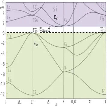
Fig. 4: Energy-band structure of the indirect semiconductor silicon 28. Conduction (EC) and valence (EV) band region are highlighted in color
Those emerging eigenstates are usually not degenerated. In a solid with
~1023 atoms cm-3 the discrete eigenstates of the single atoms are split into so many new eigenstates so that these can be treated as a continuum.
Consequently, the energy bands of a crystal are formed.
Fig. 4 shows the energy-band structure of Si. The band below the energy gap EGap is called the valence band EV. The conduction band EC is located at higher energy. For Si, the conduction band is located close to the X point in the <100>-direction. Thus, it is not at the same point in the k-space as the minimum of the conduction band. Therefore Si is called an indirect semiconductor.
2.1.4 Comparison of organic and inorganic semiconductors
The opto-electronic properties of organic and inorganic semiconductors differ in many aspects. The underlying reasons are found on the atomic scale.
Inorganic semiconductors form several eV wide valence and conduction bands, due to the strong bonding among atoms. Transitions between them
Inorganic semiconductors
17
dictate the optical absorption. Strong coupling also implies high charge carrier mobility in the order of 103 cm2 Vs-1 with carrier mean free path length exceeding interatomic spacing by far. In organic semiconductors weak coupling between the strongly chemically bonded molecular building blocks define the physical properties. Consequently, the molecular building blocks retain their identity. Valence and conduction bands are small, in the order of several hundred meV 29,30 and the charge carrier mobility is in the range of 1 cm2 Vs-1. Furthermore, inorganic semiconductors have high dielectric constants of 10and the binding energies of the Wannier-like excitons are in the order of 10 meV. Exzitonic effects are only noticeable at low temperatures and optically generated charges at room temperature can be considered as intrinsically free. In organic semiconductors the dielectric constant is in the order of 3-4 and the coulombic binding energy of the electron-hole pair is larger than kBT at room temperature. Electron-hole pairs confined to a single molecule (Frenkel excitons) have to overcome the excitonic binding energy which is in the range of 1 eV 31. As a consequence, absorption and luminescence spectra resemble those of the molecular building blocks
Tab. 1: Comparison of crystalline silicon, amorphous silicon and the prototypical organic semiconductor crystalline anthracene. Please note that the range of values for mobility and dielectric constant is due to the anisotropic properties of the different crystal directions in anthracene, while variations in a-Si are caused by different preparation methods or sample history.
crystalline
silicon (c-Si) amorphous
silicon (a-Si) anthracene (C14H10)
type indirect indirect excitonic
EGap(T=300 K) [eV] 1.12 23 1.1 - 1.8 32 4.1 31 mobility e/h [cm2/Vs] 1500/450 23 0.003- 0.8
/ 10-4 32
0.39 - 1.73 / 0.73 - 2.07 32 exciton binding energy
[eV] 15.01×10-333 - 1.0 34
melting temperature
[K] 1688 23 1420 35 489.0 32
density [g/cm3] 2.328 23 2.21 36 1.28 32
dielectric constant 11.9 23 - 2.9 - 4.11 32
Organic semiconductors
18
2.2 Organic semiconductors
Fig. 5: a) Polyethylene and Benzene as examples for conjugated systems with an alternating single and double bond system. b) sp2 hybridized carbon atoms feature three sp2 orbitals in a common plane and the perpendicular pz-orbital.
c) In ethylene, H2C = CH2, two sp2 orbitals form the σ-bond between two adjacent carbon atoms. The pz orbitals form the delocalized π-bonds. In d) the energetic relations of the bonds in ethylene are sketched (* denotes antibonding character of some orbitals). EGap is connected to lower excitation energy of the weakly bound π-system.
modified by crystal effects. Generally, organic molecular and polymeric semiconductors are hydrocarbon-based compounds in which the electrons form a conjugated system of alternating single and double-bonds. This alternating bonding sequence either forms the backbone of a polymer or the aromatic ring system of polycyclic hydrocarbons (see Fig. 5). In both cases we can distinguish between two types of chemical bonding, the σ-bonds and the π-bonds (or π-electrons). The σ-bonds are formed from the sp2 hybrid orbitals of two neighboring C atoms or from the sp2 hybrid orbital of one C atom and the 1s orbital of an H atom in a common plane. The π-bonds are formed by the pz orbitals and are oriented perpendicular to plane of the sp2 hybrid orbitals.
Organic semiconductors
19
The σ-bonds are strongly localized and form the skeleton of the molecule due to the strongly reduced energy compared to the four valence electrons of the free carbon atom. The spatial extent of a pz orbital is small and therefore only form weakly bonds compared to σ-bonds. However, these bonds form the delocalized π-electron system. Since the π-electrons are only weakly bound, they have the lowest electronic excitation energy of the molecule. The ground-state electron-occupied π-orbital with the highest energy (highest occupied molecular orbital, HOMO) and the unoccupied π orbital with the lowest energy (lowest unoccupied molecular orbital, LUMO) are of particular importance for the semiconducting properties of these materials. To be more specific, the energy difference between HOMO- and LUMO-states gives rise to the band gap of the material and enables optical light absorption and emission.
2.2.1 Bonding forces in organic semiconductors
The physical properties of an organic crystal are not only determined by the features of its building blocks. The interactions between molecules determine the structure of a crystal and are therefore fundamental to the understanding of properties like charge carrier mobility. The following section will discuss the forces leading to the crystallization between neutral and nonpolar molecules.
Attractive forces
The interaction between neutral and nonpolar molecules is related to the interaction between two permanent dipoles |𝑝⃗1|and |𝑝⃗2| with a distance r from each other. For a parallel orientation the interaction can be described as follows 37:
𝐹 = −𝑑𝑉
𝑑𝑟 = − 1 4𝜀0𝜋
6|𝑝⃗1||𝑝⃗2|
𝑟4
(6) where𝜀0 denotes the dielectric constant.
Organic semiconductors
20
A similar attractive force is developed between a permanent dipole and a polarizable nonpolar molecule. The nonpolar molecule has a polarizability α due to the large π-conjugated electron system. The electric field of the permanent dipole causes an induced dipole moment |𝑝⃗𝑖𝑛𝑑|proportional to the electric field |𝐸⃗⃗|, resulting in the attractive force 37
𝐹 = −4𝜀1
0𝜋
6|𝑝⃗1||𝑝⃗𝑖𝑛𝑑|
𝑟4 = −4𝜀1
0𝜋 6|𝑝⃗1|
𝑟4 𝛼|𝐸⃗⃗⃗|=− 1
(4𝜀0𝜋)2
12|𝑝⃗1|2𝛼
𝑟7
(7)
and their potential energy 37 𝑉 = − ∫ 𝐹𝑑𝑟
𝑟 0
= − 1
(4𝜀0𝜋)2
2|𝑝⃗1|2𝛼
𝑟6 = − 𝐴
𝑟6
.
(8) A similar term can be derived between two neutral, nonpolar molecules without a permanent molecular dipole. The cause for the van der Waals force or dispersive force is the fluctuating dipole moment due to temporarily fluctuations in the charge distribution on a very short time scale. These fluctuating dipoles induce dipoles in neighboring molecules resulting in an attractive force according to 37:𝐹 = − 1 (4𝜀0𝜋)2
𝐴′𝛼2
𝑟7
.
(9)Thefactor 𝐴′ is specific to the molecule and takes form and symmetry of the molecule into account. The corresponding potential is proportional to 𝑟−637 :
𝑉 = − 1 (4𝜀0𝜋)2
𝐴′𝛼2
6𝑟6
.
(10)As a consequence, the dispersive forces between organic molecules is short range and weak compared to other forces, e.g. ionic interactions (see Tab. 2).
Organic semiconductors
21
Repulsive forces
Additionally to the attractive forces, repulsive forces become significant at very small distances. These forces are caused by the Pauli or Coulomb repulsion of the electrons and prevent the collapse of the crystal. Often the Lennard-Jones potential is used to describe the sum of attractive and repulsive potentials as an effective potential 37:
𝑉 = 𝐵 𝑟12− 𝐴
𝑟6
.
(11) B and A are empirical constants. The minimum energy position defined by 𝑑𝑉⁄𝑑𝑟= 0 determines the equilibrium distance 𝑟0.Tab. 2: Comparison of different molecular interactions [taken from 38].
interaction proportionality of potential to distance r
typical bond energies kj mol-1
ion-ion r-1 250
ion-dipole r-2 15
dipole-dipole
(permanent) r-3 2
dipole-dipole (induced) r-6 0.2
dispersion r-6 2
Organic semiconductors
22
2.2.2 Polythiophene semiconductors
Fig. 6: Examples of poly-thiophenes: Poly(thiophene-2, 5-diyl) (PTh), poly(ethylenedioxythiophene) (PEDOT), head-to-tail coupled poly(3- alkylthiophene-2, 5-diyl) (HT-P3AT). R illustrates the possibility of different alkyl chain lengths in P3ATs.
Unsubstituted polythiophenes (PTh) are insoluble materials which cannot be processed from solution. PTs with substituents such as alkyl chains are soluble in common organic solvents and have been widely studied. PTs are intrinsically semiconducting and a variety has been explored for the use in different application, e.g. organic field effect transistors 39, organic light emitting diodes 40 and organic solar cells 41. Poly-thiophene and the probably most common representatives are shown in Fig. 6. P-doped poly(3,4- ethylenedioxythiophene) is already used in an industrial scale in capacitor electrodes and as an antistatic material. Sufficiently long alkyl side-chains on poly(3-alkylthiophenes) provide the solubility needed for processing and head- to-tail coupling of the polymer repeating units helps to promote self-assembly of a microcrystalline structure.
2.2.3 Self-assembled microcrystalline polyalkylthiophenes
Weak van-der-Waals interactions are the attractive forces in molecular crystals. Taking into account the strong repulsive forces one can expect the molecules to crystallize in an ordered dense packed structure. Packing coefficients, the volume of molecules in the unit cell in relation to the unit cell, range in the order of 0.68 (benzene) up to 0.80 (perylene
)
37. The optimumOrganic semiconductors
23
packing for molecular crystals consisting of oligacenes, e.g. naphtalene or anthracene, is reached in a “herringbone” structure, consisting of two molecules in the unit cell. This packing takes into account that seemingly planar molecules have a structure due to the electron cloud around them. The positions of the atoms in the molecule correlate to “hills” and the space in between to “valleys”. In the densest packing structure the positions of these
“hills” is subtended to the positions of “valleys” in the neighboring molecules.
This principle can be transferred to related organic materials; in this case polyalkylthiophenes. The cofacial --stacking of this material class, which will be described in more detail in the next paragraph for poly(3- hexylthiophene-2, 5-diyl) (P3HT), is subjected to the same binding forces as described above. As a consequence, two neighboring polymer chains are shifted parallel to each other along the polymer chain by one thiophene ring.
Thereby the direct facing of sulfur atoms in neighboring chains with its high electron density is avoided.
2.2.4 The crystalline structure of poly(3-alkythiophene)
P3HT belongs to the class of P3ATs with hexyl side chains (C6H13) attached to the 3rd position of every thiophene ring (see Fig. 6). For head-to-tail repeating units of the monomer, the formation of a lamellar structural order has been observed for solution processed thin-films. These polymers with a lamellar - stack show a phase separation. Highly ordered domains are embedded in an amorphous matrix and the behavior is usually referred to as semi-crystallinity.
The portion of crystalline and amorphous regions in the film is strongly dependent on preparation conditions 42, molecular weight 43, or solvents 44. The crystalline regions promote the charge transport in the material due to the highly delocalized -conjugated system of the coplanar polymer chains. These ordered domains are formed by the alignment of planarized and cofacial-stacked polymer chains with a --interaction in the [010] - crystallographic direction of the orthogonal unit cell (see Fig. 7). Along the [100] - direction the spacing is determined by the hexyl side chain.
Consequently, this value changes for other P3ATs with different chain
Organic semiconductors
24
Fig. 7: Sketch of the crystalline structure for P3HT and correspondig unit cell parameters [values taken from 45].
length 45,46. In the case of P3HT, the largest spacing between the polymer backbones prevents --interaction. In the crystalline structure, the [001] - direction is formed by the planar backbone of the polymer. High resolution structural measurements reveal that ordered domains occur as fibril or needle-like structures. The planar poly-thiophene backbones are oriented perpendicular to the long axis of the fibril. Furthermore, the contour length of the polymer correlates with the fibril width for low and medium molecular weight polymer materials 47. In disordered domains ring-to-ring torsion and kinks along the polymer chain disrupt the - conjugation of the backbone, leading to a wide distribution of conjugation length.
The current notion of high-performance, high-mobility P3HT features a microstructure in which the well-conducting and crystalline regions are bridged by single polymer strands. The connectivity between adjacent ordered parts helps to overcome the energetic offset between crystalline and amorphous regions. Hence, high mobility polymers comprise a microstructure with a sufficiently large crystalline fraction, creating a network to sustain an efficient charge transport 48–50.
Organic semiconductors
25
Fig. 8: Sketch of the P3HT morphology for a) fully amorphous and b) high performance layer consisting of amorphous and crystalline regions. Nearby crystalline regions are bridged by single polymer strands [taken from 50].
2.2.5 Absorption of visible light in linear -stacked polyalkylthiophenes Absorption of photons in the energy range of visible light is connected to an interaction in with the outer shell electrons, the valence electrons of the atoms.
The time scale, in which the absorption occurs is about 10-15 s. The vibrations of atomic nuclei occur on a time scale of 10-12 s. The positions of the atomic nuclei are not changed during the absorption of visible light. The absorption of a photon with an energy h by a polymer/molecule is similar. The molecule needs to have excitable energy states of the corresponding photon energy h= 𝐸𝑛− 𝐸0. Here, En and E0 denote an excited state and the ground state, respectively (see Fig. 5 d): -*-transition). From a quantum mechanical point of view, the transition between the two energy states causes a change in the charge distribution and therefore to a change of the dipole moment. The absorption is allowed, if the transition dipole moment is nonzero. The rate of transition kif between an initial state i and a final state f is described by the well-known Fermi´s golden rule 51:
𝑘𝑖𝑓 =2𝜋
ℏ |〈Ψ𝑓|ℋ′|Ψ𝑖〉|2𝜌
.
(12)Organic semiconductors
26
ℋ′ describes the perturbing Hamiltonian that causes the transition, e.g. the absorbed light, and ρ is the density of final states. With the complete molecular wave function Ψ𝑡𝑜𝑡𝑎𝑙 = Ψ𝑒𝑙Ψ𝑠𝑝𝑖𝑛Ψ𝑣𝑖𝑏 and the dipole operator, 𝑒𝑟̂, for the Hamiltonian we obtain 51:
𝑘𝑖𝑓 =2𝜋
ℏ 𝜌|〈Ψ𝑒𝑙,𝑓|𝑒𝑟̂|Ψ𝑒𝑙,𝑖〉|2|⟨Ψ𝑠𝑝𝑖𝑛,𝑓|Ψ𝑠𝑝𝑖𝑛,𝑖⟩|2|⟨Ψ𝑣𝑖𝑏,𝑓|Ψ𝑣𝑖𝑏,𝑖⟩|2 . (13)
Spins would only be affected by the magnetic component of light and are therefore neglected. The nuclei are to slow to response to interact with the disturbance. As a consequence, the dipole operator only affects the electronic factor (see 13). However, the macroscopic intensity of absorption depends
Tab. 3: Transitions and corresponding optical absorption [taken from 52] transition type absorption
region [nm] extinction coefficient [mol-1 cm-1]
* 100-200 103
n* 150-250 102-104
* 102-104
isolated -bonds 180-250 conjugated -bonds 220-IR
n* 1-400
isolated groups 220-320 conjugated segments 250-IR
Organic semiconductors
27
Fig. 9: Energetic positions of molecular orbitals (not to scale) and possible transitions induced by absorption. - and -transitions occur on the same molecule, n denotes possible transitions from non-bonding orbitals. * marks non-binding character of some orbitals.
on all three factors. If the value for the integral 〈Ψ𝑒𝑙,𝑓|𝑒𝑟̂|Ψ𝑒𝑙,𝑖〉 is different from zero, a transition is dipole-allowed, if not the transition is dipole- forbidden. Furthermore, the value of the integral is connected to the overlap of the final and initial wave functions. Transitions rates of orbitals located on the same molecule ( -*-transitions or -*-transitions) have higher overlaps than transitions involving molecules on different sites. Examples are charge- transfer (CT) transitions or transitions from nonbonding n orbitals, which are located on heteroatoms like oxygen, nitrogen or phosphorus. Possible transitions always occur from a ground state to a higher energy *- or *- orbital. The possible transitions are summarized in Fig. 9. Furthermore, the value of the integral will increase for well extended orbitals as the value for the transition dipole increases. As a consequence, absorption and fluorescence intensity increases with oligomer length 53. The optical properties of different transitions are compared in Tab. 3. The value for the spin integral
⟨Ψ𝑠𝑝𝑖𝑛,𝑓|Ψ𝑠𝑝𝑖𝑛,𝑖⟩ is either 0 if the spin of the initial and final state differ or 1 if they are equal. Hence, only transitions between triplet states or
Organic semiconductors
28
Fig. 10: a) Schematic of the Franck-Condon principle (r = 0 during transition). Transition arrows indicate how the overlap of the vibrational wave functions can determine the shape of the absorption. b) Absorption spectrum with vibrational transitions indexed.
singlet states are spin-allowed. However, fluorescence is an experimentally observed luminescence originating from the T1S0 transition. To explain this spin-forbidden transition, one has to take spin-orbit coupling into account. The interested reader is referred to 54.While the electronic part of (13) controls the intensity of the transition, the integral ⟨Ψ𝑣𝑖𝑏,𝑓|Ψ𝑣𝑖𝑏,𝑖⟩ is responsible for the shape. Absorption takes place from the zeroth vibrational level of the ground state into one of the vibrational levels of the excited state. Typical quantization of vibrational energy levels is in the order of 100-300 meV 51. As shown in Fig. 10 the potential energy curve of the excited state Si is displaced by ri along the binding distance axis r. A descriptive explanation is quite straightforward. In the excited state the one electron of the molecule is elevated to an antibonding orbital, leading to a reduced electron density between the atomic cores and therefore a larger equilibrium distance (see section 2.2.1). The intensity of the absorption correlates with the overlap of the vibrational wave functions ⟨Ψ𝑣𝑖𝑏,𝑓|Ψ𝑣𝑖𝑏,𝑖⟩ and the integral of the Franck-Condon-overlap. The square |⟨Ψ𝑣𝑖𝑏,𝑓|Ψ𝑣𝑖𝑏,𝑖⟩|2 is called the Franck- Condon-factor F and describes the probability for a transition from the 0th
Organic semiconductors
29
vibrational level of the ground state to the mth vibrational level of the excited state 51:
|⟨Ψ𝑣𝑖𝑏,𝑓|Ψ𝑣𝑖𝑏,𝑖⟩|2 = 𝑆
𝑚!𝑒−𝑆 . (14)
S is the Huang-Rhys-parameter, which describes the coupling of an electronic transition to a vibrational excitation. For a stiff molecule with rigid bonds and a small displacement r, usually, the 0-0´ transition is dominant. For a more flexible molecule higher vibrational molecules can form the peak with the highest intensity (see Fig. 10b).
In amorphous films or solutions these peaks of the superposed vibronic transitions are not visible. An inhomogeneous broadening of the
-*-transition due to a wider distribution of conjugation lengths at a lower mean chain length is the reason 55. In crystalline regions polyalkylthiophenes chains are planarized with a board-like system of extended polymer backbones. The degree of planarity and therefore effective conjugation length is dependent on molecular weight 48, choice of solvent 56 and temperature 57. As an example, the thermochroism in P3ATs, which is a pronounced hypsochromic shift with heating, was explained by an increasing twist between neighboring thiophene rings. The twist out of planar configuration of the backbone is accompanied by a reduced effective conjugation length what in turn leads to the blue shift in the absorption spectrum.
Current-voltage characteristics and solar cell parameters
30
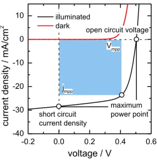
2.3 Current-voltage characteristics and solar cell parameters
-0.2 0.0 0.2 0.4 0.6
-40 -30 -20 -10 0 10
current density / mA/cm2
voltage / V
illuminated
dark open circuit voltage
short circuit current density
maximum power point jmpp
Vmpp
Fig. 11: Example of a current density – voltage (j(V)) curve in the dark and under illumination
The most important parameter describing the performance of a solar cell is the maximum power conversion efficiency, , which is defined as the ratio between the maximum power point Pmpp and the incident radiation power PL58:
𝜂 =𝑃𝑚𝑝𝑝
𝑃𝐿
.
(15)Pmpp can be calculated from characteristic parameters of the solar cells, i.e. the open circuit voltage VOC, the short circuit current density jSC, and the fill factor FF. The values for these parameters can be determined from the j(V)-curve under illumination as presented in Fig. 11. VOC is defined as the intercept with the voltage axis at which no net current is flowing. The short circuit current density is the current flowing under illumination without an applied external voltage. The fill factor describes the ration between the maximum power and
Current-voltage characteristics and solar cell parameters
31
the product of VOC and jSC. The fill factor describes the “squareness” of the j(V)-curve. Equation (15)can be rephrased as 58:
𝜂 =𝑃𝑚𝑝𝑝
𝑃𝐿 =𝑉𝑚𝑝𝑝∙ 𝑗𝑚𝑝𝑝
𝑃𝐿 =𝑉𝑂𝐶∙ 𝑗𝑆𝐶∙ 𝐹𝐹
𝑃𝐿
.
(16)Vmpp and jmpp term the current density and voltage at the maximum power point.
The parameters VOC, jSC and FF are ultimately limited by the material`s properties making up the solar cell. An upper limit for the open circuit voltage of a solar cell is obviously the band gap. Lower values are caused by recombination processes in the material. Additionally, unavoidable black body radiation at room temperature limits VOC and what is known as the detailed balance limit 27. A less general case will be explained in the following.
Assuming a pn-junction in thermal equilibrium, the net current flow is zero and the Fermi-energy is constant 58 and we obtain:
𝐸
𝐹(𝑝)0= 𝐸
𝐹(𝑛)0= 𝐸
𝐹0.
(17)The Fermi-energy is closer to the valence band edge in the neutral region at the p-type doped side (𝐸𝐹(𝑝)0 ) and closer to the conduction band edge in the neutral region in the n-type doped side (𝐸𝐹(𝑛)0 ) of the p/n-junction (see Fig.
12 a). In alignment, both values have the energy EF0. By forming a contact of the two materials, a diffusion current of holes flows from the p-side into the n-side and electrons from the n- inte the p-side, respectively. the current leads to the evolution of a space charge region (SCR) and an increasing potential difference between p- and n-side until the drift current due to this field compensates the diffusion current. As a result the band diagramm with the electrostatic potential UD shown in Fig. 12 is formed. UD depends on the doping densities in NA and ND in the respective semiconductor and can be calculated to 58:
Current-voltage characteristics and solar cell parameters
32
Fig. 12: a) Alignment of the Fermi-energy of contacted p-type and n-type doped semiconductors in thermal equilibirium. b) Schematic band diagram of a pn-junction in the thermal equilibrium. UD denotes the diffusion potential of a pn-junction.
𝑈𝐷 =𝑘𝐵∙ 𝑇
𝑞 ∙ 𝑙𝑛𝑁𝐴 ∙ 𝑁𝐷
𝑛𝑖2
,
(18)where ni is the intrinsic charge carrier density. UD is the upper limit of the open-circuit voltage for a pn-homojunction when only diffusion currents are taken into account. Furthermore, higher doping densities of the p- or n-doped semiconductor or of both and the use of materials with lower intrinsic charge carrier densities will lead to an increase in VOC. However, the useful doping range is limited by intrinsic processes, e.g. radiative or Auger recombination.
For NAND = 1032 cm-6 a value of 693 mV is the calculated limit of VOC by assuming diffusion currents only as the restricting factor. This limitation is the reason why silicon heterojunctions replaced the homojunction in terms of efficiency.
The a-Si:H/c-Si heterojunction – a brief introduction
33
2.4 The a-Si:H/c-Si heterojunction – a brief introduction
1E-4 1E-3 0.01 0.1 1 150 300
-6.5 -6.0 -5.5 -5.0 -4.5
-4.0 interface passivation layer
CB
VB (p)a-Si:H
binding energy / eV
x / µm
(n)c-Si
(n+)a-Si:H
EF
Fig. 13: Energy level alignment of an a-Si:H/c-Si heterojunction solar cell as calculated by the numerical device simulator AFORS-HET 59 using a n-type c-Si substrate and a p-doped a-Si:H emitter layer. Charge carrier selectivity is additionally achieved by the asymmetric band offsets provided by the (p)a- Si:H emitter and the (n+)a-Si:H backside (back-surface field).
A device design which needs to be presented in an own chapter is the amorphous silicon/crystalline silicon (a-Si:H/c-Si) heterojunction.solar cell, often sloppy termed silicon heterojunction (SHJ). The a-Si:H/c-Si heterojunction combines thin-film techniques with Si wafer technology for a high-efficiency concept. Currently, this cell type holds the power conversion efficiency record for Si wafer-based solar cells. Panasonic presented a large area cell with 25.6 % 60, which is close to the theoretical limit of 29 % for a c-Si based solar cell 61. The device combines a high band gap amorphous semiconductor, e.g. amorphous silicon, with a crystalline silicon absorber. The resulting band lineup of such a device is sketched in Fig. 13. The advantage of this concept is the high VOC potential. While the highly doped emitter regions in homojunctions limit the open circuit voltage to about VOC = 650 mV.
The a-Si:H/c-Si heterojunction – a brief introduction
34
Fig. 14: Simulated dependency of the open circuit voltage VOC and the efficiency on the integrated interface state density Dit at the a-Si:H/c-Si interface [taken from 62].
Heterojunctions have a much higher open circuit voltage potential.
Consequently, the Panasonic record cell demonstrated a VOC of 740 mV 60. To achieve its full potential, the defect density of the surface must be kept low.
Usually this can be achieved by an intrinsic interface passivation layer with a thickness of a few nanometers. The quality of this intrinsic interlayer is detrimental for the efficiency of a-Si:H/c-Si heterojunctions, as can be seen in Fig. 14. In this study, Dit is varied by three orders of magnitude. For Dit < 5×1010 cm-2 the VOC remains almost constant. An increase in Dit to 2×1012cm-2 rapidly decreases VOC to 560 mV. Moreover, the efficiency is reduced simultaneously from 19.8 % to 15.6 %. The results of this simulation can be easily tested by fabricating two devices, one with a high Dit and one with a low Dit. The high quality passivation was realized with a hydrogenated intrinsic amorphous silicon layer, which is known for its excellent interface passivation properties 63,64. For the low quality passivation a simple natural oxide was used with Dit of 2×10¹² eV-1cm-2 at midgap. The full distribution of the defect states regarding its energetic position in the band gap is shown in section 4.1. The consequence of the different interface passivation qualities is
The a-Si:H/c-Si heterojunction – a brief introduction
35
Fig. 15: j(V)-curves of spot test cells to determine the influence of passivation layers on the device performance in a-Si:H/c-Si heterojunction solar cells.
directly represented in the j(V)-curves displayed in Fig. 15. The VOC values differ by 110 mV, reaching VOC,a-Si = 669 mV for the high quality passivation with an a-Si interlayer and VOC, SiOx = 558 mV for the low quality passivation by means of a tunneling SiOX layer. These spot test cells nicely verify the results of the simulation with a higher VOC for the low Dit than expected from the simulation. Additional a decrease in current and fill factor is observed, which can also be explained by the recombination at the interface 62,65. The high diffusion lengths in crystalline silicon also make the devices sensitive on recombination on the back side. In this field free part of the wafer the band offsets prevent the charges from reaching the recombination active contacts (see also section 4.2). The a-Si:H/c-Si heterojunction is the successful combination of a low bandgap absorber and an amorphous wide band gap emitter and therefore very close to the device design of the hybrid heterostructure solar cells investigated in this thesis and may be of help to understand the physics behind the devices fabricated from the combination of organic and inorganic materials.
0.0 0.2 0.4 0.6
-20 -15 -10 -5 0
low
quality passivation
current density / mA cm-2
voltage / V
VOC= 110 mV
high quality passivation
The a-Si:H/c-Si heterojunction – a brief introduction
36
37
3. Experimental methods
In the present chapter measurement methods used in the thesis will be briefly explained. The focus is put on the measurement methods used for the material characterization or which require a certain knowledge regarding the analysis techniques. Among those are surface photovoltage spectroscopy, x-ray diffraction spectroscopy, photoelectron spectroscopy, charge carrier lifetime measurements, and Fourier-transform infrared spectroscopy.
Surface photovoltage measurements
38
3.1 Surface photovoltage measurements
Surface photovoltage (SPV) is a well-established electrical characterization method for the determination of the density of surface states (Dit) 66 or the equilibrium band bending in silicon 67. Surface photovoltage measurements utilize the change of the electrochemical potential in the space charge region of a semiconductor due to illumination with light of suitable wavelength and intensity. A metal-insulator-semiconductor (MIS) structure is formed between the transparent conductive oxide (TCO) layer on a glass plate, an insulating mica plate and the c-Si sample (see Fig. 16) 68. The ohmic back contact is realized through a gold-coated chuck. The sample is excited by laser pulses (t = 150 ns, = 900 nm, PLaser = 210 W) through the TCO layer. The absorption of the laser light in the semiconductor (here Si) gives rise to the change of the surface potential due to a redistribution of photogenerated charges, which is measured as a change in the capacitance of the MIS structure. Ideally, the laser intensity is high enough to create as many excess charge carriers to reach flat-band condition in the semiconductor and is in a steady state after the laser pulse is turned off. In that case, the maximum value of the SPV signal at the time t = 0 (immediately following the laser pulse) gives the band bending in the dark that has to be corrected by the Dember voltage 69,70. The investigation of the energetic distribution of interface states Fig. 16: Schematic sketch of the
surface photovoltage
measurement setup including a band scheme of c-Si. A MIS structure is formed between a TCO on a glass plate, the insulating mica plate and the c-Si sample (taken from 68).
X-ray diffraction spectroscopy
39
(Dit) is possible by applying an external bias voltage to the sample to change the energetic position of the Fermi-level 66.
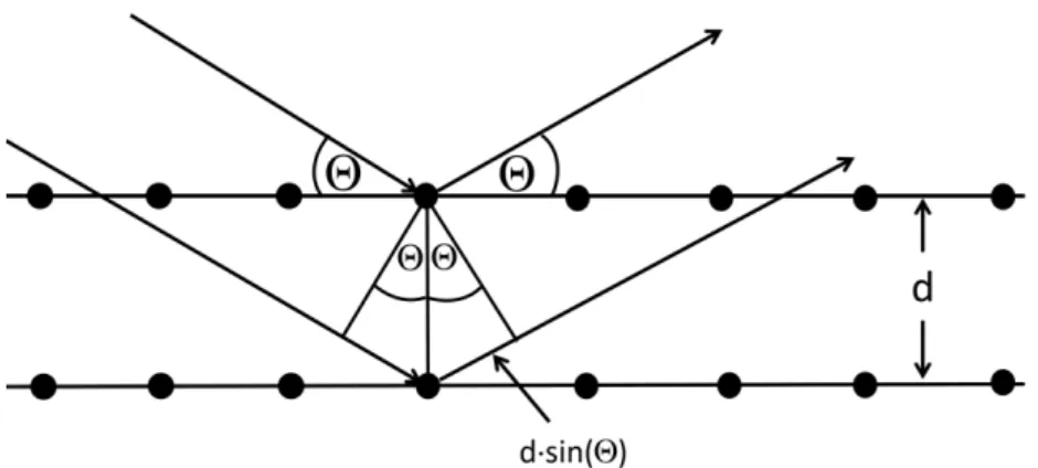
3.2 X-ray diffraction spectroscopy
X-ray diffraction spectroscopy (XRD) allows defining the material composition and the structural quality, including the orientation of the crystallographic direction. An x-ray beam incident to the sample includes an angle of to the lattice plane (see Fig. 17). This beam is deflected at the lattice planes and interferes with x-ray beams deflected from the neighboring lattice plane with the distance d. The angle for constructive interference of the incident x-rays to occur is determined by Bragg´s law 71
2𝑑 ∙ 𝑠𝑖𝑛(Θ) = 𝑛 ∙ 𝜆
.
(19)The prerequisite for constructive interference is a integer multiple n of the x- ray´s wavelength . Similar to the ideal grating, Bragg-peaks become sharper and higher order peaks evolve with an increasing number of lattice planes N.
Additionally, The width of the first order peak is proportional to N-1. From the width of the first order peak the crystallite height B can be estimated using Scherrer´s equation 72,73:
𝐵 = − 0.9 ∙ 𝜆
cos (Θ) ∙ √(∆Θ)2− 𝑏2
.
(20)∆Θ is the half width of the Bragg peak and b the peak broadening due to instrumental contributions. Here, a value of 0.07° is assumed limiting the validity of the Scherrer´s equation to crystallite heights of ~150 nm. Another limitation is that the equation is only valid for thin films with a finite number of lattice planes and may not be used for thick crystals.
The samples were measured in a Bragg-Brentano-geometry with a SEIFERT theta-theta-diffractometer MZ VI using Cu-Kα = 0.154056 nm radiation and a secondary monochromator to filter undesired reflections.
Photoelectron spectroscopy
40
Fig. 17: Deflection of irradiated x-ray beams including the angle and the optical retardation d×sin() to describe Bragg`s law.
3.3 Photoelectron spectroscopy
Photoemission is based on the photoelectrical effect, which was first observed by Hertz 74 and explained by Einstein 75. Classically, it is described as a three step process 76:
Photo excitation of electrons
Their transport to the surface and
The escape over their work function barrier (surface) into vacuum Ideally, electrons are not subjected to inelastic scattering until their escape into vacuum. These electrons carry the desired information about their initial state within the distribution of their kinetic energies. Monochromatic radiation is used for the excitation to define the amount of energy transferred to the electrons. Usually energy-selective detection is employed. The reference energy is the detector vacuum level EVac relative to which the kinetic energy Ekin of photoelectrons is detected. Sample and detector are electrically connected and therefore the Fermi energies are aligned (not the vacuum levels). The binding energy Ebind is measured relative to the Fermi energy.
photoelectron spectroscopy is frequently used to determine the energy level alignment of molecules/polymers
![Fig. 7: Sketch of the crystalline structure for P3HT and correspondig unit cell parameters [values taken from 45 ]](https://thumb-eu.123doks.com/thumbv2/1library_info/5658045.1694307/24.892.138.686.125.431/fig-sketch-crystalline-structure-correspondig-parameters-values-taken.webp)

![Fig. 14: Simulated dependency of the open circuit voltage V OC and the efficiency on the integrated interface state density Dit at the a-Si:H/c-Si interface [taken from 62 ]](https://thumb-eu.123doks.com/thumbv2/1library_info/5658045.1694307/34.892.180.650.127.404/simulated-dependency-circuit-voltage-efficiency-integrated-interface-interface.webp)
![Fig. 19: Universal curve of the mean free path of electrons in solids dependent on their kinetic energy [taken from 79 ]](https://thumb-eu.123doks.com/thumbv2/1library_info/5658045.1694307/42.892.201.639.133.496/universal-curve-electrons-solids-dependent-kinetic-energy-taken.webp)


