01–05 September 2019 Berlin l Germany
www.microscopy-conference.de
Organized by
© Sergii Figurnyi l Fotolia.com
ABSTRACTS
MS 6: Nanostructured materials (particles, 2D-materials, porous materials) ... 243
MS 7: Ceramics, oxides and minerals ... 320
Instrumentation and Methods (IM) IM 1: Advances in instrumentation, software ... 342
IM 2: Phase-related techniques (holography, ptychography, phase plate, DPC, COM, beam shaping) . 393 IM 3: In-situ, environmental, time-resolved electron microscopy ... 447
IM 4: Quantitative TEM/STEM, simulation, new software developments, diffraction ... 513
IM 5: Low energy electron microscopy (STEM, TEM, SEM) and FIB-techniques ... 576
IM 6: Spectroscopy (EELS, EDX) ... 611
IM 7: 3D and analysis of big data ... 656
Life Sciences (LS) LS 1: Single particle, cryo-TEM... 685
LS 2: Pathology, pathogens and diagnostics ... 697
LS 3: Imaging of large volumes ... 729
LS 4: Cyro and plastic section tomography on biological samples ... 737
LS 5: Correlative and multimodal microscopy ... 755
LS 6: Probes and localization techniques ... 776
LS 7: Advances in sample preparation ... 785
2
PL.01
Proteins in whole cells studied with liquid-phase electron microscopy
N. de Jonge1,2, D. B. Peckys3, I. N. Dahmke1, S. Keskin1
1INM-Leibniz Institute for New Materials, Saarbrücken, Germany
2Saarland University, Physics Department, Saarbrücken, Germany
3Saarland University, Department of Biophysics, Homburg, Germany
Transmission electron microscopy (TEM) has traditionally been associated with the study of thin solid samples in vacuum. With the availability of reliable thin membranes of silicon nitride, TEM of liquid specimens has become accessible (1). The usage of liquid-phase scanning transmission electron microscopy (STEM) presents a novel concept to study membrane proteins within whole mammalian cells in their native liquid environment (2). The cells in liquid are placed in a microfluidic chamber enclosing the sample in the vacuum of the electron microscope, and are then imaged with STEM. It is not always necessary to enclose the cells in the microfluidic chamber. For many studies, it is sufficient to obtain information from the thin outer regions of the cells, and those can be imaged with high resolution using environmental scanning electron microscopy (ESEM) with STEM detector (3). A third option is to cover a liquid specimen under a thin membrane of graphene providing the thinnest possible layer (4). The obtained spatial resolution is typically limited by ration damage (5). An advantage in liquid is that the electron dose tolerance of the sample is improved by an order of magnitude in liquid compared to samples in ice under the right conditions (6).
Liquid-phase STEM was used to explore the formation of HER2 homodimers at the single-molecule level within intact SKBR3 breast cancer cells in liquid (3). HER2 is a membrane protein and plays an important role in breast cancer aggressiveness and progression. Data analysis based on calculating the pair correlation function from individual HER2 positions (Figure 1) revealed remarkable differences in its functional state between rare- and bulk cancer cells with relevance for studying the role of cancer cell heterogeneity in drug response. We discovered a small sub- population of cancer cells with a different response to a therapeutic drug (7). The same approach to study the spatial distribution of HER2 is now also available for the study of biopsy samples from patients.
Other membrane proteins have been studied as well, such as calcium channels. Here, we aimed to determine the composition of the protein complex from its subunits, and monitor differences with location in the plasma membrane and with functional state.
References:
(1) de Jonge, N. and Ross, F.M.Nat. Nanotechnol. 6, 695-704 (2011) (2) de Jonge, N., et al. Proc. Natl. Acad. Sci. 106, 2159-2164 (2009) (3) Peckys, D.B., et al. Sci. Adv. 1, e1500165 (2015)
(4) Dahmke, I.N., et al. ACS Nano 11, 11108-11117 (2017) (5) de Jonge, N., et al. Nat. Rev. Mater. 4, 61-78 (2019)
(6) Keskin, S. and de Jonge, N. Nano Lett. 18, 7435-7440 (2018) (7) Peckys, D.B., et al. Mol. Biol. Cell 28, 3193-3202 (2017)
This work is supported by DFG under SFB1027 and by the Else Kröner-Fresenius-Stiftung.
Fig: 1: Liquid-phase STEM of HER2 proteins in SKBR3 breast cancer cells. A) Overview STEM-Image at 800 x magnification. B) STEM image recorded at the position of the yellow square in A, at 60.000x magnification, showing the abundance of quantum dot labeled HER2 molecules; the labels in B were automatically detected and outlined in yellow. C) Pair correlation function g(r) analysis of all label positions in B indicating HER2 homodimer formation at a distance of r= 20 nm.
4
PL.03
Visualizing membrane dynamics with electron microscopyVisualizing membrane dynamics with electron microscopy
S. Watanabe1
1John Hopkins School of Medicine, Department of Cell Biology, Baltimore, MD, United States
Cell membranes undergo constant remodeling, and these morphological changes must be visualized to study processes such as synaptic transmission. However, it is difficult to capture these changes with precise temporal and spatial resolution. To address this problem we have combined optogenetics with electron microscopy to develop a high-resolution, time-resolved technique called flash-and-freeze. Using flash-and-freeze we have discovered a fast endocytic process in neurons called ultrafast endocytosis.
Neurons communicate via neurotransmitter release. Upon stimulation, synaptic vesicles fuse with the synaptic plasma membrane and release their contents. However, the number of synaptic vesicles is limited in the mammalian neurons and vesicles must be regenerated quickly. Based on 40 years of work, clathrin-mediated endocytosis is thought to be responsible for synaptic vesicle regeneration. However, clathrin-mediated endocytosis is too slow to match the speed of fast synaptic transmission. To directly capture fast membrane remodeling events during synaptic transmission, we used flash-and-freeze. We expressed channelrhodopsin, a light-gated cation channel, in mouse hippocampal neurons.
A brief flash of blue light triggers sodium influx and generates an action potential, leading to synaptic activity. Neurons are then fixed by high-pressure freezing at defined time points after the action potential, ranging from 15 ms to 10 s, to capture morphological changes by electron microscopy. Using this approach, we found that membranes are internalized within 50-300 ms. Owing to its unmatched speed, we termed this process ultrafast endocytosis.
This new electron microscopy technique, flash-and-freeze, combines optogenetics and high-pressure freezing to generate time-resolved, high-resolution images of any cellular process. Using this approach, we have discovered ultrafast endocytosis, a mechanism for rapid membrane recycling at chemical synapses, and probed the underlying molecular mechanisms. However, flash-and-freeze could be applied to study other fast cellular events with combined spatial and temporal resolution unmatched by any other technique.
advantageously when investigating semiconducting materials, if one carefully chooses the primary energy (PE) of the e-beam.
In this work, we show a novel way for a quick exploration of fabrication defects in solution-processed organic field effect transistors (OFET).
The OFET device examined in this work is built with the n-type (electron-transporting) small-molecule material TAPP1, which is zone-cast on top of a dielectric polymer layer. It is first imaged in an epi-illumination light microscope (LM) and then at different, rather low voltages in a novel prototype SEM, the DELTA (Carl Zeiss Microscopy) which has spatial and chromatic aberration correction.2
In the LM the TAPP layer shows a feather-like pattern, incomplete coverage of the area between source and drain, and inhomogeneity in thickness.
To examine its electron-transporting ability, a negatively charged surface layer on TAPP is created by PE=50 eV.
Several places between source and drain, where charges cannot quickly dissipate, are found (Fig. 1, left). Although an e-beam with a higher energy (PE=1000 eV) can also generate negative charging (Fig. 1, right), no defects can be visualized, probably due to the much larger interaction volumes of the incident electrons. A weak positive charging is achieved at PE=100 eV, which may allow investigation of hole-transporting. The critical energy point E2 (no charging/charge equilibrium3) for this crystalline TAPP layer is found at PE=200 eV. Here a well-resolved image using a slow scan rate is obtained. Islands and narrow passes (Figure 2), which lead to a charge accumulation or a slow dissipation, are easily detected.
Dynamic imaging of a semi-conductor layer at different landing energies around the charge-neutral E2 point allows easy detection of defects within the layer. By image processing, e.g. binary thresholding, the effective area of the TAPP layer that actually contributes to OFET performance may be calculated. Thus, the measured electron-transport mobility can be corrected. Electron-microscopic investigation in terms of charge transport mobility is underway.
References:
(1) C. Martens, U. Zschieschang, H. Wadepohl, H. Klauk, L.H. Gade,Chem. Eur. J. 2012, 18, 3498 (2) Steigerwald, Frontiers of Characterization and Metrology for Nanoelectronics 2013
(3) Reimer, Image Formation in Low-voltage Scanning Electron Microscopy. SPIE Optical Engineering Press 1993 The authors thank the DFG for funding (SFB 1249)
Fig. 1: Surface charging of the TAPP layer in an OFET device under different PEs: negative charging at PE=50 eV and 1000 eV, positive charging at PE=100 eV and free of charging at PE=200 eV, scale bar 10 µm.
Fig. 2: Fabrication defects exposed at PE=50 eV (left) and imaged at PE=200 eV (right), scale bar 10 µm.
6
Fig. 1
Fig. 2
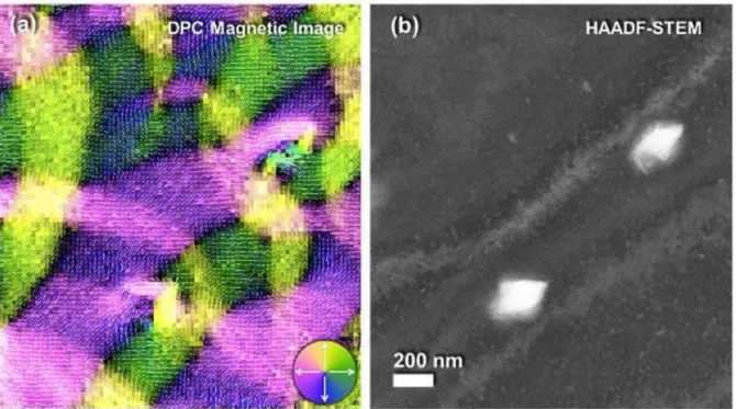
to be fully understood. We have previously shown qualitative in situ Lorentz transmission electron microscopy (TEM) images of FeRh thin film where the magnetic domain walls are identified during the AF-FM transition (3). In this work, we have used differential phase contrast (DPC) for quantitative magnetic imaging of a FeRh thin film, with local Rh- rich precipitates, where the local magnetization intensity and orientation is determined. To investigate the dynamics of the AF-FM transition, in situ heating was carried out using a Gatan heating holder inside an aberration-corrected TEM in zero magnetic field by turning off the objective lens of the TEM; with a measured stray field value of 0.01 mT. DPC images were obtained in scanning TEM (STEM) mode with a pixelated detector (4). Fig.1a shows a DPC image of a relatively large area of the thin film. A HAADF STEM image (Fig.1b) was subsequently obtained, with the objective lens back on, from the same area to correlate the formation and the final orientation of magnetic domains to the local distribution of Rh-rich precipitates. Our results give new perspective in correlating the magnetic domain evolution and stabilization with the crystallographic structure and coherent inhomogeneities of the FeRh thin film.
References:
(1) Ralf Witte et al., Physical Review B, (2016) 93, 104416.
(2) Ralf Witte et al., Journal of Physics D, (2017) 50, 025007.
(3) Saleh Gorji et al, Microscopy and Microanalysis, (2018) 24 (S1), 934-935.
(4) Matus Krajnak et al., Ultramicroscopy, (2016) 165, 42–50.
Fig. 1:a) a DPC magnetic image of FeRh thin film after transition from antiferromagnetic to ferromagnetic at around 130 °C. Color wheel and arrows indicate the magnetization orientation. b) a HAADF-STEM image of the same area at room temperature.
Fig. 1
8
MS1.003
Strain measurement of finFET device using moiré fringes by scanning transmission electron microscopy
Y. Kondo1, N. Endo1, Y. Aoyama1, C. C. Lin2, K. Hsu2
1JEOL Ltd., EM business unit, Tokyo, Japan
2IST Inc., Material analysis division, Hsinchu, Taiwan
Recently, a device structure has become three dimensional (3D). A typical 3D structure in modern device is a finFET, which has a tri-gate structure (1). In other aspects, strained silicon is used to enhance the mobility of carriers.
Typically, channel strain in pMOS of the finFET is arisen by pinching the channel with stressors made of typically Si/Ge. Measurement of the channel strain is important because it relates to device performance. However, we have difficulties in measuring the strain due to the structure of finFET. First, the channel is sandwiched with gate electrodes.
The channel strain must be measured in such a direction that the electron beam scans across these layers. Second, the sample thickness must be more than 100 nm to avoid strain release (2). This paper reports how we measure the strain of the finFET by scanning transmission electron microscopy (STEM). We measured the strain by a method that utilizes moiré fringes of STEM, (3,4,5), which arise as a result of undersampled lattice fringes with the raster of STEM.
Sample made by focused ion beam was 150 nm thick. The pitch of fins in this sample was ~ 50 nm, so three fins were included in the thickness. The lamella was cut along the channel direction so that we can observe the strained channel pinched between Si/Ge stressors. The measured moiré fringe was arisen as a result of undersampling of lattice (0.192 nm, Si [220]). The moiré fringes of the targeted lattice was selectively extracted, since it works as a real space frequency filter and filters out the other lattices having different spacing and directions.
Figure 1 (a) shows a bright field STEM image of the sample observed at 200 kV. The black area is overlapped with the W electrode, and the grey area is a sandwiched with double-layer of the TiNx gate electrode of and an SiOxNy
insulator. These elements were confirmed from 3D elemental volume map by 3D EDS (energy dispersive X-ray spectroscopy) tomography. We could not observe the moiré fringe under the W electrode due to its heavy absorbance of electrons. Thus, we measured the channel strain from the area surrounding the W wire, which is indicated by a pink square in Fig. 1(b). Figure 1(b) shows a strain map of the (220) lattice, which is along the channel direction (X- direction). The line profile of the strain along the pink square is shown in Fig. 1(c). Finally, the compressive strain of the channel pinched between Si/Ge stressors was measured to be - 0.7 - 0.9%.
The STEM moiré method can be applicable to measure the strain of finFET, since the STEM moiré fringes act as a spatial filter in real space and extract only the target lattice. This method can be applied to measure the strain of the target volume surrounded by other materials. In addition to this, the nature of the real space filter leads the capability to detect dislocations that are intrinsically fatal for device manufacturing.
References:
(1) D. Hisamoto et al., Int. Electron Devices Meeting, (IEEE, 1989), p. 833.
(2) S. Kim et al., AIP Advances 3, 092110 (2013).
(3) N. Endo and Y. Kondo, Proc. 32th LSI Testing Symposium, (2012), p73.
(4) S. Kim et al., Appl. Phys. Lett. 102 (16), 161604 (2013).
(5) N. Endo and Y. Kondo, Microsc. Microanal. 20 (S3), 1068 (2014).
Fig. 1: Results of strain analysis by STEM moiré method. a) X-cut view of a finFET device. The gate and W wire overlap the Si channel. b) Strain map along channel of finFET. c) Profile of strain map along the pink square shown in (b).
10
MS1.005
Atomic resolution differential phase contrast imaging of defect structures in heteroepitaxial GaAs grown on Si
3N
4nanohole-masked Si(001)
J. Bürger1,2, T. Riedl1,2, T. Langer1,2, A. Trapp1,2, D. Reuter1,2, J. K. N. Lindner1,2
1Paderborn University, Department of Physics, Paderborn, Germany
2Center for Optoelectronics and Photonics Paderborn (CeOPP), Paderborn, Germany
Differential phase contrast (DPC) imaging is a promising technique in scanning transmission electron microscopy allowing for the visualization of electric and magnetic fields. With a probe Cs-corrected microscope equipped with a DPC detector electric fields in the vicinity of defects or at interfaces of polar mismatched materials are measurable at atomic resolution. III-V semiconductors like GaAs form a variety of defects when grown on a silicon substrate due to a high lattice, thermal expansion and polarity mismatch. In the optimization of GaAs-based optoelectronic devices DPC opens a whole new field of defect detection and characterization possibilities.
Heteroepitaxial GaAs grown on Si(001) forms defects like dislocations, stacking faults, nano-twins and even anti- phase boundaries close to the GaAs-Si heterointerface. Some of the above mentioned defects exhibit polar terminations allowing differential phase contrast imaging for the detection of their extension and position as well as their electronic properties. Therefore, DPC images of nano-twins, stacking faults bounded by partial dislocations and anti-phase boundaries are captured. By comparison with HAADF-STEM, BF- and DF-TEM the nature of these defects can be analyzed and the influence of Bragg contrasts on the DPC signal can estimated. In addition, electric fields at the Si(001)/GaAs heterointerface are analyzed and quantified.
A nanohole-patterned Si3N4 film acts as a trap for threading defects in the heteroepitaxial GaAs grown on Si(001) substrate. The patterning is accomplished by nanosphere lithography in combination with reactive ion etching and wet-chemical cleaning, leaving nanoholes with diameters of about 70 nm in Si3N4. The removal of surface oxides prior to solid source MBE growth of GaAs is achieved by an in-situ atomic hydrogen treatment. A 30 nm thin cross-section specimen, which is prepared by mechanical dimple grinding and argon ion polishing, is analyzed with a probe Cs- corrected JEOL JEM-ARM200F microscope equipped with an 8-fold segmented annular detector for DPC imaging.
For the characterization and determination of the defects BF-/DF-TEM, EFTEM, STEM-HAADF and STEM-DPC images with a resolution down to 70 pm are employed.
The above mentioned misfit-related defects concentrate close to the GaAs/Si(001) heterointerface. Nano-twins, stacking faults and anti-phase boundaries are analyzed by DPC imaging revealing the electric field and charge distributions in vicinity of the defects (Fig. 1). At the Si(001)/GaAs interface a shift of the beam perpendicular to the interface is seen, which can be ascribed to the polar/non-polar transition and related charge redistribution at the interface.
Differential phase contrast STEM imaging is well suited to analyze defect structures in polar semiconductors and at heterointerfaces. At medium resolutions defects can be elegantly visualized but care must be taken on the influence of Bragg contrasts. DPC images at atomic resolution show characteristic features for each analyzed type of defect.
Fig. 1: (a) Cross-section DPC image of GaAs grown selectively in the opening of a Si3N4 mask on Si(001). Nanotwins are marked with dotted white lines, while white arrows highlight fields at the heterointerface.(b) A DPC image of a stacking fault is shown in the inset. Atomic column positions are determined from the corresponding HAADF-STEM image and marked by white dots.
12
MS1.006
Correlation of structural modifications and switching characteristics by multiscale phase mapping in filamentary type HfO
2-based RRAM
A. Zintler1, R. Eilhardt1, S. Petzold1, N. Kaiser1, S. Ulhas1, L. Alff1, L. Molina-Luna1
1Technische Universität Darmstadt, Materials- and Earth Science, Darmstadt, Germany
Hafnia based resistive random access memories (RRAM) are candidates for next generation nonvolatile memory due to their potential for fast, dense and energy efficient data storage and proven compatibility to CMOS technology (1).
According to the current state of understanding, the resistive switching (RS) behavior relies on the electric field driven formation and dissolution of oxygen deficient nanoscale conducting paths, so called "filaments" (2). The effects behind this mechanism includes accelerated diffusivity and inter band-gap states located at possible grain boundaries (GBs) as well as interfacial redox processes.
By using HR-STEM imaging and Automated Crystal Orientation Mapping (ACOM) we were able to analyze the nanoscale grain structure of the multilayer and the arrangement of the m-HfO2 grains in the TiN/HfO2/Pt stack which is deposited on a c-cut Al2O3 substrate.
In an attempt to achieve a forming free RRAM device, the texture of the HfO2 thin film was controlled by a reactive molecular beam epitaxy synthesis routine. The proposed methods allow characterization of the texture transfer of the substrate texture to the TiN electrode thin film and finally to the dielectric layer.
EBSD and XRD data (not shown) indicates the TiN grains grow with the (111) axis parallel to the surface normal (001) of the c-cut Al2O3 and the HfO2 layer exhibit (11-1) as their out-of-plane axis. High-resolution ACOM (Fig.1b) allows a detailed analysis of the set of existing in-plane rotations for the m-HfO2 phase. For a single grain of the TiN bottom electrode a set of three HfO2 grains is observed (Fig.1c-d). Fig.2b shows GBs in the dielectric layer which connect top and bottom electrode. The importance of the GBs also arises due to localized electronic inter-bandgap states (3) and the reduced defect formation energies at GBs (4). Due to preferable diffusivity at GBs, the proposed interface reactions (5) were also accessible by EELS mappings (not shown).
These physical properties strongly suggest that the initial dielectric breakdown and consequent conducting path formation occurs at the grain boundary. In our electric field dependent in situ TEM studies (6), we demonstrated for the first time how to electrically contact and operate a device fabricated in a FIB. The RS behaviour of the electron- transparent lamella were comparable to a conventional reference device (Fig.2c).
References:
(1) S.U. Sharath et al., Adv. Funct. Mater, 27 (2017).
(2) R. Waser et al., Adv. Mater., 21 (2009).
(3) K.-H. Xue et al., Appl. Phys. Lett., 102 (2013).
(4) K. McKenna and A. Shluger, Appl. Phys. Lett., 95 (2009).
(5) G. Niu et al., Mater. Res. Lett., 7 (2019).
(6) A. Zintler et al., Ultramicroscopy, 181 (2017).
The authors acknowledge financial support from the Deutsche Forschungsgemeinschaft (DFG) under research grant MO 3010/3-1 and the European Research Council (ERC) "Horizon 2020" program under grant No. 805359-FOXON.
Fig. 1: a. TEM image of the MIM stack. b. ACOM phase and orientation mapping of a. c-d. PFs derived from the ACOM dataset.
Fig. 2: a. SEM image of a FIB prepared HfO2 device on a MEMS based chip used for in situ biasing TEM experiments, 1: contact for bottom TiN electrode, 2: top Pt electrode. b. Corresponding HAADF-STEM image of the stack. c. Unipolar RS behavior of a bulk device (purple/black dotted curve), unipolar reset of the prepared lamella device (blue curves).
14
MS1.008
Hollow-cone Foucault imaging of magnetic microstructures in large magnetostrictive FeGa alloy
A. Kawaguchi1, A. Kotani1, K. Harada1,2, H. Numakura1, Y. Ishii1, S. Mori1
1Osaka Prefecture University, Department of Materials Science, Naka-ku, Sakai, Osaka, Japan
2RIKEN, Hatoyama, Saitama, Japan
Magnetostrictive materials exhibit external form changes by applying an external magnetic field. Recently, FeGa alloys has attracted much attention as a practical magnetostrictive material because they exhibit a large magnetostriction at low magnetic field (1). It is suggested that the magnetostriction of FeGa alloy should originate from the reorientation of magnetoelastically and magnetostatically autarkic rigid micro-"cells", and thus, dynamical behaviors of the magnetic domain structures by applying external magnetic fields should have strong relationship with the large magnetostriction in FeGa alloys. In this study, we have investigated the magnetic microstructures of large magnetostrictive FeGa alloys by using Lorentz microscopy, hollow-cone Foucault imaging (2) and small-angle electron diffraction techniques (3).
Figure 1(a) shows magnetic microstructures obtained using Fresnel method in the (001) plane of the FeGa thin film without external magnetic fields. In the Fresnel image, bright and dark lines identified as magnetic domain walls can be clearly seen. Thus, we determined spatial distribution of magnetization in each magnetic domains by SmAED and Foucault images. In Fig. 1(a), yellow arrows indicate the direction of the magnetizations in each magnetic domains.
The 180° and 90° magnetic domains are formed at room temperature without external magnetic field. Note that magnetic moments are oriented along the (100) direction. When a magnetic field of 400 Oe is applied perpendicular to the film, it is found that the magnetic moments should rotate in the in-plane direction toward the (010) direction and the magnetic domains with magnetization along the (100) direction are dominant at the expense of magnetic domains with the magnetic moments along the (001) direction. In addition, SmAED experiments revealed that the magnitude of the magnetization remains intact. These unusual magnetic responses of magnetic domains to the external magnetic field should be important for better understanding of the large magnetostrictive effect in FeGa alloys. In this presentation, we will also report the development of hollow-cone Foucault imaging method.
References:
(1) C. Harsh, et al., Nature 521, 340–343 (2015).
(2) K. Harada et al., Applie Physics Express (in press).
(3) H. Nakajima et al., Microscopy, 67, 207–213 (2018).
Fig. 1:
firstly deposited on quartz substrates by molecular beam deposition. Laser lights (wavelength: 532 nm, energy density: 1.6 x 10⁹ W/m2) were irradiated on the samples. Here, laser irradiation time (tirr) was varied from 0.67 to 3.0 μs. Samples were characterized by microscopic Raman spectroscopy (facility designed by PHOTON Design corp.), and electron back scattered diffraction (EBSD) method (JEOL JSM-7000F with EBSD detector designed by TSL solutions corp.).
Fig. 1(a) shows Raman signals measured at surface of GeSn thin film before and after LA (tirr: 1.5 μs). We can see clear peak around 300 cm-1 due to Ge-Ge atomic bond after LA, which supports that GeSn film has been successfully crystallized by LA. Peak intensity and full width at half maximum (FWHM) of Raman signals are summarized as a function of tirr in Fig. 1(b). Interestingly, we can clearly see that the peak intensity of Raman signal measured from GeSn film increases with increasing tirr, while that of Ge film shows little dependence on tirr. Moreover, we can also say that FWHM of the Raman peak measured from GeSn samples decreases with increasing tirr, while that of Ge film showed little dependence. From these results, we can say that crystallization of GeSn film proceeds with increasing tirr, while that of Ge film has little dependence on tirr.
To discuss the growth feature of GeSn films, EBSD measurements were carried out. Mapping images of Ge and Sn signals are summarized in Fig. 2 as a function of tirr. Here, we can clearly see the Sn crystal signals for all tirr, while Ge crystal signal does not appear for short tirr. These results strongly suggest that crystallization of GeSn occurs following to Sn precipitation, due to the low solid solubility of Sn in Ge (~1%), and that such Sn precipitation triggers the crystallization of GeSn. This is a very interesting finding in the field of GeSn crystal growth. Detailed physics will be discussed with more supporting data during the presentation.
References:
(1) D.W. Jenkins and J.D. Dow, Phys. Rev. B 36, 7994 (1987).
(2) S. Gupta, Y.-C. Huang, Y. Kim, E. Sanchez, and K.C. Saraswat, IEEE Electron Device Lett. 34, 831 (2013).
16
Fig. 1
Fig. 2
superconducting networks can be fabricated. Compared to traditional methods for NWs growth, such as vapor−liquid−solid (VLS), SAG allows a change of geometry from vertical nanowires to an in-plane growth of NW networks, with a large number of NW interconnections (1-3).
SAG was realized on a (100) GaAs substrate. PECVD grown SiOx was patterned using electron beam lithography and wet etching. A GaAs(Sb) buffer was grown on the substrate and a second InGaAs buffer was grown on top of the first one. The buffered geometry allows for substantial elastic strain relaxation and a strong enhancement of field effect mobility. InAs wires with triangular cross-sections were grown by molecular beam epitaxy (MBE). The Al was grown in-situ by MBE using angled deposition covering one of the facets.
Figure 1 shows the morphology of the SAG NWs. Figure 1 (a) is a SEM image of four NWs grown in-plan on the GaAs substrate. Figure 1 (b) is a magnified SEM image of one of the NWs, acquired at 52°, showing the truncated central (1-10) facet surrounded by the three (111) facets of InAs. Figure 1 (c) and (d) are an illustration of the NW cross section and the corresponding FIB cut, showing the buffered layer structure and the triangular InAs NW.
The quantum device performance of the individual SAG NWs are affected by the atomic arrangement in the heterostructures and particularly at the interface between the individual NWs and their buffer. The interface is therefore investigated at the atomic level using HAADF-STEM images acquired from a FIB lamella containing the NWs. The composition of the different layers is measured by STEM-EDX and EELS, while the strain is measured from atomic resolved images using Geometrical Phase Analysis (GPA).
Atomic resolved STEM images of the InGaAs/InAs interface are shown in Figure 2, corresponding to a FIB cut from a (100) oriented in-plane NW. In this segment, we observe an epitaxial interface with no defects. This is the ideal case, however, the overall structure contains a low density of defects and dislocations, which affect the device performance and reduces the conductivity.
In order to improve the device performance, the growth of the InGaAs second buffer has to be optimized in terms of growth rate and temperature, with the aim of eliminating atomic defects and achieve the best quantized conductance.
References:
(1) Krizek, Filip, et al. Physical Review Materials2.9 (2018): 093401.
(2) Aseev, Pavel, et al. Nano letters19.1 (2018): 218-227.
(3) Vaitiekėnas, S., et al. Physical review letters121.14 (2018): 147701.
Fig. 1: (a) SEM image of four in-plane SAG NWs acquired at 0° and (b) of a magnified NW acquired at 52°. (c) Illustration of the SAG NW cross section. (d) FIB cross section.
Fig. 2: HAADF STEM images of InGaAs/InAs interface at increasing magnification, showing an epitaxial interface.
18
Fig. 1
Fig. 2
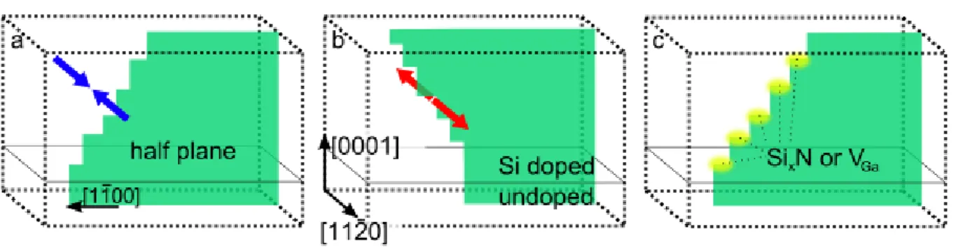
lattice energy by strain release (1,2). The other approach is that Si hinders the growth of the dislocation half plane for edge and mixed type TDs (3). As the GaN growth on sapphire takes place under tensile strain these two models lead to opposite directions of TD inclination with respect to the half plane position as shown in Fig. 1 (b,c).
The goal of our experiment was to find the correlation between the inclination direction and the half plane position of TDs in Si-doped GaN layers in order to clarify the origin of the inclination. A Si-doped and an undoped GaN layer grown by MOVPE on a sapphire substrate were examined. Scanning transmission electron microscopy (STEM) analysis showed a broad distribution of inclination directions of the TD lines around the reported <1-100>-direction in the Si doped GaN layer (Fig. 2). However, in undoped GaN the TDs incline mainly into <11-20>-directions. Using tilting series in low magnification STEM and high resolution STEM we show for the first time that the half plane size is decreased by the inclination due to Si-doping. This indicates a hindering of the half plane growth and favours the inclination model shown in Fig. 1c. It further explains the increase of tensile strain in GaN as well as the reduction of compressive strain in AlGaN on AlN by Si introduction. Additional inclination into the <11-20>-directions in doped and undoped GaN takes place simultaneously. This explains the distribution of the inclination directions in Si-doped GaN.
References:
(1) M. A. Moram, Journal of Applied Physics 109 (2011), 073509 (2) K. Forghani et al., Journal of Applied Physics 112 (2012), 093102 (3) A. Dadgar et al., Applied Physics Express 4 (2011), 011001
Fig. 1: Different models for TD inclination and the resulting inclination direction. Strain driven, surface mediated climb in a) compressively and b) tensely strained layers. c) Model of TD inclination caused by SixN masking.
Fig. 2: a) Distribution of TD inclination directions in doped and undoped GaN grown on sapphire (m and a correspond to <1-100> and <11-20> directions). b) Cross-section ADF STEM image showing TD inclination in Si-doped and undoped GaN.
Fig. 1
20
Fig. 2
represents high and low resistive states. However, micro and nanostructural changes, especially those which are connected to structural vacancies, play a decisive role in multilevel data storage applications
Our study focuses on the micro- and nanostructural changes occurring by heating an amorphous Ge6Sn2Sb2Te11 thin film. Therefore in situ TEM and XRD studies were performed to reveal nano- and microstructural changes. These structural changes are correlated to changes in the electrical properties of the material.
Ge6Sn2Sb2Te11 represents Sn substituted Ge8Sb2Te11 which is used as storage medium in blue-ray discs. Thin amorphous films of Ge6Sn2Sb2Te11 were deposited by sputtering and phase changes were investigated by in situ XRD and TEM measurements. Further temperature dependent resistivity measurements were performed ex situ using the van der Pauw method.
Besides the amorphous phase three different crystalline phases were observed which can be separated by their unique distribution of structural vacancies on cationic sites.
At 112 °C the films started to crystallize. In the temperature range of 112 °C – 130 °C a so far for Ge8Sb2Te11
unreported (pseudo) cubic phase with statistically distributed structural vacancies was observed.
At ~ 130 °C structural vacancies start to order and form vacancies layers. It could be demonstrated for the first time that these ordering processes are associated with a domain growth/coalescence process.
At ~ 260 °C a gradual transition to a trigonal phase with van der Waals gaps is observed. It could be demonstrated that an in plane movement of defects, so called bi-layer defects, largely increases the structural order of the materials.
This mechanism was recently proposed but so far could not be observed directly by means of in situ observations.
The temperature dependent resistivity measurements revealed an extra intermediate resistive state which appears in the same temperature region with sole presence of the strongly disordered (pseudo) cubic phase.
In summary, micro and nanostructural changes in amorphous Ge6Sn2Sb2Te11, were studied in detail by in situ XRD and TEM heating experiments. The formation of a pseudo cubic phase lead to the presence of an extra intermediate resistivity state.
References:
(1) C.Koch, T.Dankwort et al., Acta Materialia, 152, 2018
22
MS1.P005
Characterisation of Crystalline Defects in As-Transformed and Hot-Deformed τ-MnAl Alloys using Weak-Beam Dark Field Imaging
P. Zhao1,2, K. Nielsch1,2, T. G. Woodcock1
1IFW Dresden, Institute for Metallic Materials, Dresden, Germany
2TU Dresden, Dresden, Germany
The L10-ordered, thermodynamically metastable phase τ-MnAl exhibits a high uniaxial magnetic anisotropy, high magnetisation and contains no critical elements, making it a highly promising rare-earth free permanent magnetic material. The thermal stability of the τ-phase at high temperatures could be improved through the addition of carbon, however, the low coercivity currently achieved (<10% of the anisotropy field) is still the main obstacle for the real application of MnAl magnets. Studies have found that the extrinsic magnetic properties (remanence, coercivity and energy density) could be greatly improved through hot deformation compared to the as-transformed state. If detailed knowledge about defects in both as-transformed and deformed τ-MnAl-C alloys is obtained, further improvements, particularly in coercivity, could be made, as defects interact with magnetic domain walls. In this study, various defects including dislocations, stacking faults, twin boundaries and grain boundaries have been characterized in both as- transformed and deformed τ-MnAl-C alloys by transmission electron microscopy (TEM) using weak-beam dark-field analysis or bright/dark field image analysis. The results revealed that the density of these defects are very sensitive to the sample state, stacking faults and dislocations decreased greatly in the deformed samples. In addition, the decreased grain size in the deformed τ-MnAl-C sample may be the main reason for the improvement of coercivity due to pinning of domain walls at grain boundaries. Further studies about the atomistic structure and elementary segregation at these defects should be investigated in order to deep our understanding about the interaction of magnetic domain walls and these defects.
Magnetic Skyrmions are a potential candidate for future data storage and spintronics applications. The first experimental discovery was done with Small Angle Neutron Scattering (SANS) from the bulk chiral B20 material MnSi at temperatures below 30K, where a hexagonal lattice of skyrmions was evidenced (1). With a Transmission Electron Microscope (TEM), magnetic skyrmions can be conveniently observed in real space using phase related techniques like Lorentz-TEM (LTEM), electron holography or Differential Phase Contrast (DPC) microscopy (2,3,4).
To approach a technological application, skyrmion hosting materials with a Tc well above room temperature need to be investigated (5). Microscopic classification includes the skyrmion size, magnetic phase diagram with respect to temperature and applied magnetic field as well as topological charge density determination.
In this work multilayer systems of Pt/Co/W and Pt/Co/Tb stacks are investigated. Due to the interfacial Dzyaloshinskii- Moriya interaction, Neel-type skyrmions are present in these systems. Therefore, a sample tilt is required to image the skyrmions. LTEM and DPC is used to characterize the skyrmion size in combination with magnetic phase simulations.
The magnetic phase diagram and topological charge map is studied with LTEM using a liquid nitrogen holder.
The magnetic phase diagram is retrieved and for the case of field increase from zero field, the skyrmions are generated as topological remnants of the stripe phase (Fig. 1 (a)-(d)). The magnetic contrast is shown for DPC and LTEM and is in agreement with contrast simulations. Using those the actual skyrmion size is related to the observed contrast. As an example for LTEM, the contrast for a single skyrmion is shown for three different sample tilt angles in Fig. 1 (e)-(g). The contrast profile along the tilt axis is taken and compared to simulations in Fig. 1(h).
LTEM and DPC are suitable methods to characterize Room Temperature skyrmion samples. The size is best evaluated using the in-focus technique DPC. The increased contrast of LTEM compared to DPC makes it the best tool to quickly sample the magnetic phase diagram.
References:
(1) Mühlbauer S., et al., Science 323, 915 (2009) (2) Yu X. Z., et al., Nature 465, 901 (2010)
(3) Park H., et al., Nat. nanotechnol. 9, 337 (2014)
(4) Schneider S., et al. Phys. Rev. let. 120, 217201 (2018) (5) Pollard S. D., et al., Nature commun. 8, 14761 (2017)
Fig 1: LTEM image of (a) the magnetic labyrinth domains at zero field, (b) extended domains with residual stripe domains and skyrmions, (c) magnetic skyrmions and (d) reduced number of magnetic skyrmions due to increased field. (e)-(g) Sample tilt series for a single magnetic skyrmion. (h) Image profile along skyrmion contrast and included contrast simulations.
24
Fig. 1
Investigations as to the cause of stable relative permittivity are presented, based on analytical scanning transmission electron microscopy (STEM) analyses of the relaxor solid solution systems: (1-x)BaTiO3 - xBi(M0.5Ti0.5)O3;M= Mg or Sc. Nanoscale compositional segregation is revealed within the perovskite phase at high levels of Mg or Sc substitution, close to the limiting compositions that give near-flat εr(T)responses. The possibility that changes in bulk polarisation in the ergodic region are supressed because of this compositional immiscibility is discussed. The STEM data, in association with εr(T) trends, imply that segregated, weakly polar Bi and Mg/Sc rich nanoregions inhibit the increase in polar order that normally occurs in a relaxor ferroelectric as it cools below the Burns temperature. Based on these findings, a final overview of options for developing Bi-free materials with similar levels of performance, but which are compatible with industrial processes for manufacturing multilayer capacitors will be presented.
26
MS1.P008
Interface effects on the ferroelectric polarization in ultrathin PbTiO
3films investigated by ISHG and HAADF imaging
A. Vogel1,2, N. Strkalj2, M. Campanini1, C. Gattinoni2, N. Spaldin2, M. Rossell1, M. Fiebig2, M. Trassin2
1Empa Dübendorf, Electron Microscopy Center, Dübendorf, Switzerland
2ETH Zürich, Department of Materials, Zürich, Switzerland
During the last decade, a strong focus in condensed-matter physics and material science has been on the construction of atomically sharp perovskite oxide heterointerfaces. This has led to the deterministic control of ultrathin functional oxide interfaces at the atomic level, revealing novel interfacial properties, such as two-dimensional electron gases, superconductivity, ferromagnetism, and multiferroicity, which are not inherent to the individual constituents.
In ferroelectric heterostructures, atomic-scale interface engineering leads to the control of bulk properties, namely the domain state and polarization orientation. Taking uniaxial ferroelectric PbTiO3 ferroelectric thin films as model system, we investigate the emergence of the polarization in the ultrathin regime for different interfacial atomic terminations.
Using a combination of in-situ optical second harmonic generation (ISHG)(1) and aberration-corrected scanning transmission electron microscopy (STEM), we reveal the different interface contributions of the atomically controlled bottom interface and the free surface of the ferroelectric layers in the enforcement of the polarization orientation.
Specifically, two PbTiO3 thin films are grown by pulsed laser deposition on either MnO2 or LaO terminated LaSrMnO3 buffered SrTiO3 substrates. The polarization dynamics of the corresponding downwards and upwards enforced polarized films is monitored ISGH. Further, differences in the atomic structure of the PbTiO3 layers depending on the termination-sequence at the PbTiO3 - LaSrMnO3 interface are investigated by quantitative analysis of high-angle annular dark-field (HAADF) STEM images. Figure 1 shows a HAADF-STEM image of a PbTiO3 thin film along the [010] zone axis. The structural information is obtained by fitting the atomic positions using the python library atomap (2). The overlaid yellow arrows point to the polarization vector resulting from the off-centering of the Ti cation from the center of its four Pb neighbors; they are plotted opposite to the polar atomic displacements. Besides, the analysis of the strain state (tetragonality) of the two films reveals clear differences between the two PbTiO3 films.
We show that the macroscopic polarization dynamics during the film synthesis alters drastically depending on the polarization orientation of the films. The interaction of the ferroelectric surface with the growth environment results in either a strong enhancement or suppression of the macroscopic polarization of the thin films, which is driven by the choice of atomic terminations and polarization orientation. Post growth measurements of the polar atomic displacements and of the tetragonality distribution using HAADF-STEM confirm the interface impact on the internal polarization state. Our results demonstrate the interface competition in the onset of the ferroelectric state in PTO thin films in the ultrathin regime and identify routes to enhance the polarization of ultrathin films.
References:
(1) G. De Luca, N. Strkalj, S. Manz, C. Bouillet, M. Fiebig, and M. Trassin, Nat. Commun. 8, 1419 (2017) (2) M. Nord et al., Advanced Structural and Chemical Imaging 2017, 3:9
Fig. 1: (a) Polarization map calculated from the atomic displacement superimposed on a HAADF image. (b) Average atomic displacement of B-site atoms. (c) Average tetragonality of the A-site atoms.
Fig. 1
However, the lower symmetry of these 3D nanostructures compared to e.g. planar systems makes the interpretation of transmission electron microscope (TEM) images far more difficult. This work presents the use of electron tomography to circumvent the challenging interpretation of single projections of core-shell NWs.
The goal of this work is to apply electron tomography method for detecting and analyzing the morphology and chemical composition of complex 3D dot-in-a-nanowire structures based on InGaN/GaN core-shell NWs.
GaN/InGaN/GaN core-shell-shell NWs were grown on a GaN-on-sapphire (0001) template by plasma-assisted molecular beam epitaxy using a Ti nano-hole mask produced by colloidal lithography. A sophisticated focused ion- beam preparation was applied to fabricate needle-shaped specimens containing only a single NW. A tilt series of high- angle annular dark-field (HAADF) scanning TEM (STEM) micrographs with steps of 2° was recorded and used for the tomographic reconstruction. Subsequently, slices of different orientations and isosurface representations were extracted out of the 3D data to visualize and analyze the NW core-shell structure.
The isosurface representation (cf. Fig. 1) of the GaN outer shell reveals the crystal shape und surface faceting of the NW. As expected, the lower section of the NW consists of six energetically favored m-plane facets whereby the NW tip reflects a pyramidal shape being composed of s- and r-plane facets, which are, however, not perfect symmetrically positioned to each other. This asymmetry in the pyramidal tip shape is associated with the presence of an inversion domain.
Longitudinal and transversal slices (cf. Fig. 2) through the reconstruction reveal the internal (In,Ga)N shell structure.
The slices allow the complete determination of shell thicknesses and verify variations of the (In,Ga)N shell composition. The overall development of the (In,Ga)N shell morphology deviates to some extent from the expected 6- fold symmetry, which is not the case for the outer GaN shell. Moreover, the dot-in-a-nanowire structure is clearly resolved inside the NW tip by sharp increase in the indium content. The 3D form of the dot resembles an inverse truncated pyramid with distorted hexagonal base. Energy dispersive x-ray (EDX) spectroscopy is applied to compare the intensities of the tomographic slices based on HAADF contrast with EDX maps in order to discuss the sensitivity of chemical concentration in the tomographic reconstruction.
An InGaN/GaN core-shell NW has been investigated by electron tomography. The faceting and spatial distribution of the chemical composition of the NW core, shell and dot-in-a-nanowire structure is revealed unambiguously. It has been shown that the symmetry of the NW is disturbed by defect interactions. The results demonstrate that electron tomography allows insights into the evolution of the core-shell structure formation during growth.
28
Fig. 1
Fig. 2
are a topic of intense research. Here we use electron energy loss spectroscopy (EELS) to study electron-beam- induced changes in transition metal thiophosphates (TMTPs) MnPS3 and FePS3. The choice of these materials is dictated by the fact that they show both ionic and covalent bonding character (1).
FePS3 and MnPS3 layers were prepared from bulk through mechanical exfoliation. EELS spectra were acquired at 80 kV using GIF attached to a Titan 80-300. The energy resolution was determined to be 0.6 eV. We used core-loss EELS spectroscopy obtained at the S L2,3, Fe/Mn, M2,3 (2), Fe L2,3 and P L2,3 edges (3) in order to study the effects of the beam-induced damage in these two systems. In the experiments, the peak positions and the fine structures (ELNES) of these edges were monitored as a function of electron dose and exposure time. These experimental investigations were supported by density functional theory (DFT) electronic structure and EELS spectra calculations.
Figure 1 shows the changes observed at the Fe M2,3 edge of FePS3 with prolonged exposure to the electron beam. In the spectra, both shift in the peak positions as well as the changes in the peak intensity ratios are observed as a result of prolonged exposure to the electron beam. These spectral changes point towards the changes in Fe valency as a result of the beam-induced damage on the structure. Similar spectral changes are also observed at the S and P-L2,3
edges. Based on these experimental results as well as DFT calculations, we show that this is due to electron-beam- induced changes in S-S and P-S bonds.
In conclusion we have used electron energy loss spectroscopy to understand the interaction between the incident electron-beam and MnPS3 respectively FePS3 thin layers. Our EELS results point towards electron-beam-induced changes in the bonding character in these transition metal thiophosphates.
References:
(1) Brec, Solid State Ionics 22, 3 (1986).
(2) Van Aken, P. A., et al. Physics and Chemistry of Minerals7 (1999): 584-590.
(3) Laffont, L., et al. Chemistry of Materials23 (2006): 5520-5529.
Fig. 1: Fe M2,3 electron energy-loss near-edge structure in FePS3 during electron irradiation. The experiment was executed in an 80 kV Titan TEM with an energy resolution of 0.6 eV.
30
Fig. 1
To get a deeper understanding of the microstructure-property relationship in He-FIB Josephson junctions, the local microstructural modifications caused by He ion irradiation, as a function of irradiation dose D, has to be investigated.
This can be achieved by transmission electron microscopy (TEM), which requires the site-specific preparation of a TEM-lamella from the Josephson barrier region.
Epitaxial c-axis oriented YBCO thin films were grown by pulsed laser deposition (PLD) on (001)-oriented SrTiO3
(STO), single crystal substrates. For electric transport measurements, Au layers were deposited in-situ after the PLD process, and we used photolithography and Ar ion milling to prepattern 4 µm wide YBCO microbridges. Subsequently, focused ion beam irradiation was done in a Zeiss Orion NanoFab He/Ne ion microscope (HIM) with 30 keV He+ ions to fabricate the Josephson barriers. To image possible structural modifications in our YBCO films, we used scanning transmission electron microscopy (STEM). For the STEM studies, we irradiated a YBCO bridge with a series of parallel lines, using increasing doses from D = 50 to 105 ions/nm, with well-defined spacing between adjacent lines.
Subsequently we prepared a cross-sectional TEM-lamella containing all irradiated lines, by in-situ lift-out using a Ga- FIB microscope together with a micromanipulator.
We found that the critical current density jc of the He-FIB Josephson barriers decays exponentially with irradiation dose D (2). A simple explanation of the exponential decay of jc with increasing D would be a linear increase of the junction barrier thickness. The STEM analysis showed that for doses higher than D = 1000 ions/nm, highly resistive amorphous tracks appeared and their width increases roughly linear up to the highest dose D=105 ions/nm. For D = 1000 ions/nm and below, we could not identify any change in the structure of the irradiated sections.
Our STEM analysis indicates that medium doses do not induce significant structural damage of the YBCO crystal lattice, which is consistent with the assumption that the He-FIB easily moves oxygen ions from the Cu-O chains to interstitial sites (3) and thereby altering the local electric transport properties of YBCO on the nanometer scale. This observation indicates that He-FIB is a promising tool for nanopatterning (without removal of material) of YBCO films with ultra-high spatial resolution.
References:
(1) S.A. Cybart et al., Nature Nanotechnology 10, 598-602 (2015).
(2) B. Müller et al., arXiv1901.08039 (2019).
(3) E.Y. Cho et al., Appl. Phys. Lett 113, 022604 (2018)
32
MS1.P012
Analytical TEM investigation of structural changes in electrical stressed 0.25 µm AlGaN/GaN HEMTs
A. Graff1, P. Diehle1, M. Simon-Najasek1, F. Altmann1, M. Rzin2, F. Rampazzo2, M. Meneghini2, G. Meneghesso2, E.
Zanoni2, J. Grünenpütt3, H. Jung3, K. Riepe3, H. Blanck3, B. Lambert4
1FraunhoferInstitute for Microstructure of Materials and Systems IMWS , Electronic Materials and Components, Halle, Germany
2University of Padova, Information Engineering, Padova, Italy
3United Monolithic Semiconductors GmbH, Ulm, Germany
4United Monolithic Semiconductors S.A.S., Villebon sur Yvette, France
High electron mobility transistors (HEMTs) based on AlGaN/GaN heterostructure improved over the last two decades and moved into industrial use for RF power amplifiers in space and defense applications.
The stability and reliability under high dissipated power and high junction temperature should be ensured. Therefore a better understanding of degradation mechanisms limiting performance and electrical reliability is needed. In this work, we are focusing on structural failure modes of AlGaN/GaN HEMTs, related to the gate metallization, that are reducing the reliability of the devices.
The tested technology is based on GaN/AlGaN/GaN epitaxy grown by metal-organic chemical vapor deposition (MOCVD) on a SiC substrate. The studied AlGaN/GaN HEMTs are characterized by a 2x40 μm gate finger topology with a gate length of 0.25 µm. The devices have a Ni/Pt/Au Schottky gate metallization. Hot-electron characterization was carried out by means of electroluminescence (EL) microscopy where differences in the EL signal could be detected between center and rim of the transistor structures. These results are used to determine reasonable positions for the TEM cross section preparation. Three HEMTs (Samples A, B, C) were selected to investigate the structural changes at the Schottky gate after a 24h electrical test under different DC conditions (Table 1). Two TEM cross sections were prepared by FIB (Zeiss, NVision) out of each HEMT, one at the rim and one near the center of a gate finger. The cross sections were investigated in detail by means of TEM, STEM and EDX (FEI, Titan XFEG and SuperX system).
Table 1: DC 24h electrical test scenario for the three selected devices.
TEM investigations of the HEMT cross sections show structural changes in the semiconductor mainly in the barrier layer in the Schottky gate region. Here pitting into the AlGaN barrier layer could be observed at the dielectric / semiconductor interface. It is assumed that these pits are formed at position of high electrical fields. The pit formation gets more pronounced for the higher loaded HEMT structures (Fig. 1). Oxygen diffuses into the Pits during the 24h test (Fig.2).
Beside the pit formation structural changes at the metal / semiconductor interface can be observed where Ga is missing in the AlGaN layer and oxygen gets into the barrier. This Ga deficit is correlated with gold diffusion through the Pt and Ni gate metal layers to the Schottky barrier. These significant structural changes explain the measured reduction in transconductance.
The investigated AlGaN/GaN HEMTs show different level of degradation after 24 hours stress test depending on the dissipated power. The failure modes seemed to be thermally activated and enhanced by the electric field. The test results led to an improved technology qualified for space applications.
Fig. 1: HRTEM detail images of the Schottky gate edges in direction of the drain contact for sample A, B and C.
Structural changes in the AlGaN barrier layer and the metal / semiconductor interface are highlighted by red circles.
Fig. 2: Normalized distributions of selected elements out of EDX mappings after 24h DC test (Sample A, B, C).
Direction to the drain contact marked by D.
Fig. 3
34
MS1.P013
Characterization of Solution-grown and Sputtered Inx(O,S)y Buffer Layers in Cu(In,Ga)Se2-based Solar Cells by Analytical TEM
X. Jin1, R. Schneider1, D. Hariskos2, W. Witte2, M. Powalla2, D. Gerthsen1
1Karlsruhe Institute of Technology (KIT), Laboratory for Electron Microscopy, Karlsruhe, Germany
2Zentrum für Sonnenenergie- und Wasserstoff-Forschung Baden-Württemberg (ZSW), Stuttgart, Germany
Nowadays, solar cells with thin-film absorbers of Cu(In,Ga)Se2 (CIGS) are widely used and show power conversion efficiencies above 22%. For such CIGS-based cells, Cd-free materials with wider bandgap energies are required to replace the commonly used CdS buffer layer, and Inx(O,S)y has become a promising candidate among other possible materials.
In this work, TEM results are reported on CIGS-based solar cells with CdS and Inx(O,S)y buffer layers, which were prepared by either chemical-bath deposition (CBD) or sputtering. In each case, the cell has a ~2 µm thick CIGS absorber deposited on a Mo-coated soda-lime glass substrate by in-line co-evaporation of the elements. In addition, after deposition of the buffer layers the cell setup was completed by sputtering of ZnO/ZnO:Al window layers. The data obtained from the cells with Inx(O,S)y buffers are compared with those of a standard CIGS solar cell with a CBD-CdS buffer with an efficiency of ~17.8%. Moreover, the influence of the deposition temperature on the layer properties was analyzed.
In detail, the microstructure of the different buffer layers was studied by diffraction-contrast and high-resolution TEM imaging, nanobeam electron diffraction, and energy-dispersive X-ray spectroscopy was performed for chemical analysis. Both the CBD-grown and sputtered Inx(O,S)y layers show a nanocrystalline structure in contrast to larger grains in the standard CdS buffer. There are differences in the chemical composition of the Inx(O,S)y layers, i.e. the oxygen content in CBD-Inx(O,S)y is considerably higher than the applied oxygen concentration in sputtered-Inx(O,S)y.
The difference in crystalline quality of the buffers and CIGS/buffer interfaces might contribute to the different performance of the investigated CIGS-based thin-film solar cells.
Towards this goal, we investigate vanadate superlattices composed of (LaVO3)n/(PrVO3)n repetitions, where n is in terms of psuedo-cubic (PC) unit cells, using aberration-corrected scanning transmission electron microscopy (STEM).
These atomic scale studies are vital to identify changes in A-site cation ordering between the layers that could lead to improper ferroelectricity.
We study (LaVO3)n/(PrVO3)n films ~20 nm thick, for 3 ≤ n ≤ 8 and grown by pulsed laser deposition on SrTiO3, using a double aberration-corrected FEI Titan Themis 60-300 operated at 300 kV. High angle annular dark field (HAADF) image series are acquired and effects of scan drift and other distortions compensated (2). Chemical analyses are made with electron energy-loss spectroscopy (EELS), using a Gatan GIF Quantum ERS.
Figure 1 presents analyses of the n = 6 film. The A-site cations in its HAADF image (a) show the antipolar displacements of an in-plane X5– mode, as seen in all the films. Their displacements are plotted as a virtual strain in (b), whose average per row is shown in (c). By correlating to EELS data (d, e), it can be seen that the displacements are greater in the Pr-rich layers than the La-rich layers. Moreover, the contents of La and Pr cations modulate sinusoidally between the LaVO3 and PrVO3 repetitions (rather than being chemically abrupt), and the antipolar displacements vary in coincidence with these compositional fluctuations. While this result supports the working hypothesis for obtaining improper ferroelectricity, remarkably, the films with n = odd – which are also the candidates for improper hybrid ferroelectricity – systematically show a different behavior. Their layers are chemically indistinct, with strong intermixing of La and Pr cations; accompanying this, their A-site cation displacements are much more uniform across the film thickness.
The results suggest a strong interplay between the structure and composition of the vanadate superlattices. We hypothesize that the n = odd films are structurally "inhibited", pushing them to intermix. Equally, a proportional relationship is seen between A-site cation ordering and composition. We are pursuing further studies to understand these phenomena, which could have strong implications for this field.
References:
(1) J M Rondinelli and C J Fennie, Adv. Mater. 24 (2012), p. 1961.
(2) L Jones et al., Adv. Struct. Chem. Imaging 1 (2015), 8.
This work was supported by the Swiss National Science Foundation, Sinergia Project No. 154410. We acknowledge the CIME, EPFL for access to its facilities; at the CIME we thank Colette Vallotton and Danièle Laub for TEM specimen preparation.
Fig. 1: (a) HAADF image of (LaVO3)6/(PrVO3)6 film on [110]PC zone axis (substrate plane vertical); (b) corresponding εxy virtual strain map of displacements of A-site cation positions; and (c) average strain per atomic row. (d) STEM- EELS map (from another film region); (e) normalized compositional line-profile.
36
Fig. 1
![Fig. 1: Experimental and calculated 300kV TEM image of the LaNiO 3 /LaGaO 3 heterointerface in [110] projection](https://thumb-eu.123doks.com/thumbv2/1library_info/3847286.1515032/69.892.73.725.962.1169/fig-experimental-calculated-image-lanio-lagao-heterointerface-projection.webp)
![Fig. 1: (a) Schematic of an InAs island atop a GaAs nanopillar. (b,c) Maps of the [2-1-1] Lagrange strain in the plane marked in (a) for an InAs diameter of around 12 nm with one interfacial 60 misfit dislocation (arrow): (b) GPA of e](https://thumb-eu.123doks.com/thumbv2/1library_info/3847286.1515032/85.892.66.731.936.1176/schematic-island-nanopillar-lagrange-strain-diameter-interfacial-dislocation.webp)