MC 2017
Lausanne
21–25 AUGUST 2017
LAUSANNE l SWITZERLAND
Microscopy Conference
© SwissTech Convention Center / 77091969 l JiSign l Fotolia.com
PROCEEDINGS
Plenary Lectures, Ernst Ruska Lectures, Harald Rose Lecture ... 1
Material Science (MS) MS 1: Functional materials and semiconductors ... 9
MS 2: Interfaces and surfaces, coatings and thin films ... 60
MS 3: Energy-related materials ... 117
MS 4: Metals, alloys and intermetallics ... 189
MS 5: Carbon-based materials, soft matter and polymers ... 274
MS 6: Nanoparticles, 2D materials, nanocomposites and catalysts ... 314
MS 7: Ceramics, oxides and minerals ... 370
Instrumentation and Methods (IM) IM 1: Advances in instrumentation & methods ... 404
IM 2: Environmental, in-situ and time-resolved microscopy ... 553
IM 3: Image analysis and handling of big data sets ... 631
IM 4: Quantification and modelling ... 649
IM 5: Spectroscopy in microscopy ... 690
IM 6: Tomography... 712
IM 7: Phase-related techniques ... 750
Life Sciences (LS) LS 1: Single particle EM, microscopy of membrane assemblies ... 801
LS 2: From cells to tissues: Cellular electron tomography and imaging of large volumes ... 814
LS 3: Microorganisms, pathogens and EM in diagnostics... 843
LS 4: Subcellular processes in plants and animal cells... 868
LS 5: Cytoskeleton, cellular traffic and membrane dynamics ... 896
LS 6: Imaging techniques: X-ray microscopy, live/in vivo imaging and correlative approaches ... 907
LS 7: Advances in sample preparation and analysis... 952
Plenary Lectures, Ernst Ruska Lectures, Harald Rose Lecture
PL.01
The future of electron microscopy
G. Van Tendeloo1,2, S. Bals1, S. Van Aert1, J. Verbeeck1, J. Hadermann1, D. Schryvers1
1EMAT, University of Antwerp, Belgium
2NRC, Key State Laboratory, Wuhan University of Technology, Hubei, China staf.vantendeloo@uantwerpen.be
In order to look into the future of electron microscopy it is important to first look into the past: where do we come from? From the initial start with Ruska till about the eighties electron microscopy was mainly descriptive. Imaging was only in TEM, the resolution was limited to a few Angstrom and neither EDX nor EELS were really well developed. Only at the end of the 20th century and particularly after the introduction of aberration corrected imaging, scientists focused on quantitative interpretation of the results.
This is the way modern electron microscopy should further evolve in the future. Too many researchers still consider an electron microscope as a big (and expensive) magnifying glass. One should see EM as a very valuable analytical instrument, able to provide quantitative data on structure, composition and electronic structure. In that way the results can not only be used as input for theoretical predictions, but also contribute to explain and understand physical/chemical/mechanical properties of (nano)materials. In this lecture we will provide illustrative examples for this.
Another dangling problem in EM is the study of soft matter. Beam damage often hampers correct or detailed interpretation of the results. Not only polymers, but also e.g. organic solar cell materials or metal organic frameworks (MOFs) suffer from this effect. A new generation of very sensitive cameras helps to overcome part of this problem, but a correct interpretation of these highly underexposed and noisy images is not a straightforward problem and correct statistical methods/algorithms should be used in order not to induce artifacts.
Acknowledgements:
We are very grateful for collaborations with Artem Abakumov, Rolf Erni, Marta Rossell, Tom Wilhammar, Jean-Marie Tarascon, Luis Liz-Marzan, Daniel Vanmaekelbergh. Collaborators Annick De Backer, Karel Van den Bos, Thomas Altantzis, Maria Meledina and Stuart Turner are highly acknowledged. Financial support mainly was provided by FWO, IAP, ERC and European Projects ESTEEM2, ESMI and Eurotapes.
Field mapping for semiconductor research by off-axis electron holography and diffraction based techniques
D. Cooper1,2, V. Boureau1,2, B. Haas1,2, N. Bernier1,2, J.-L. Rouviere1,2
1Univ. Grenoble Alpes, Grenoble, France
2CEA, LETI, MINATEC Campus, Grenoble, France david.cooper@cea.fr
In this presentation we will provide a brief introduction discussing the motivations behind the miniaturization of semiconductor devices which leads to the requirement of transmission electron microscopy to provide characterisation. We will focus on techniques that can be used to measure fields with nanometer resolution. Off-axis electron holography which uses an electron biprism to interfere an electron wave that has passed through a specimen with one that has passed through only vacuum to form an interference pattern known as the hologram. From the hologram the modulations in electron phase can be measured from which the electrostatic potential calculated. Other techniques such as differential phase contrast and diffraction based techniques (4D STEM) can be used to recover information about the potentials from the deflection of a transmitted beam. In this presentation we will show how they can be used in a semiconductor research environment to provide useful information about dopant potentials and strain fields with nm-scale resolution.
We will compare results acquired by the different techniques on both dopant and deformation mapping.
Figure 1(a) shows a potential map of a pMOS device that has been acquired by off-axis electron holography. Although the measurement of the carrier concentration is complicated due to artifacts with specimen preparation and charging under the electron beam, the position of the electrical junction can be measured. Figure 1(b) shows a field map acquired by DPC. Here a segmented detector has been used to determine the deflection of a convergent beam as it passes through the doped specimen. In this presentation we will discuss the advantages and disadvantages of using these different techniques on different types of semiconductor specimens such as silicon CMOS devices and also IIIV materials for light emission.
Deformation is a key parameter used to improve device performance. Figure 1(c) shows a STEM image of a SiGe recessed source and drain device. Dark field electron holography has been performed on the device and deformation maps for the (d) in-plane, εx and (e) growth, εy directions can be seen. These experimental results can be compared to those obtained using precession electron diffraction shown in Figure 1(f) and 1(g) which shows deformation maps for the εx and εy directions respectively.
We will also present results obtained by switching a resistive memory device in-situ in the TEM. Different types of SrTiO3 devices have been electrically connected using a movable probe to apply a voltage to the electrode. The device is examined by combinations of STEM, electron energy loss spectroscopy (EELS) and holography to demonstrate that the movement of oxygen vacancies leads to changes in the electrical conductivity from a high resistive (HRS) state to a low resisitive state (LRS). Figure 2 shows where a resistive device has been switched and the movement of oxygen vacancies mapped with 1 nm spatial resolution by comparing the changes in the Ti L3 eg and 2tg edges which correspond to changes in the Ti – O bonds. We will discuss the experimental procedure and prospects for routine in-situ biasing experiments in the TEM.
These experiments have been performed on the platforme nanocharacterisation (PFNC) at Minatec.
We thank the European Research Council for funding Stg:305535 “Holoview”.
Figure 1. (a) Potential map of a pMOS device acquired by off-axis electron holography. (b) Field map of the same device acquired by DPC. (c) STEM image of a SiGe/Si device. (d) and (e) show εx and εy maps acquired by dark field electron holography. (f) and (g) show maps of the same device acquired using precession diffraction.
Figure 2. (a) Shows schematic of specimen examine and VI characteristics during forming. (b) and (c) HAADF STEM images of the Sr:STO active layer before and after forming. (d) and (e) Ti EELS spectra acquire across region of interest for the device in a LRS and HRS showing changes in the L3 eg and t2g peaks across the active layer. (f) and (g) maps showing the shift of the L3 2tg peak for devices in a LRS and HRS state respectively.
Cryo-electron microscopy of biological particles in vitrified water
J. Dubochet1
1University of Lausanne jacques.dubochet@unil.ch
Biological material is predominantly made out of water but water evaporates in the vacuum of an electron microscope.
Cryo-electron microscopy wants to keep water in the specimen by cooling it at a temperature where evaporation is negligible, but water freezes upon cooling and ice is as bad as no water.
Brüggeller and Mayer (1980) discovered that liquid water can be vitrified namely, it can be made solid without changing significantly its structure (so we believe). We succeeded in turning vitrification into a simple and reproducible method for preparing biological samples in a thin film of immobilised water (Adrian et al., 1984). With this method we could obtain a 3-d model of a virus at 35 Å resolution (Vogel et al., 1986).
Since then, many scientists contributed to the staggering advance of image processing; cryo-electron microscopes have been further improved for the task; lately a breakthrough was achieved with new electron detectors. Thanks to these efforts, it is now possible to achieve close to atomic resolution for single particles in vitreous water on a nearly routine basis. Improving the resolution by a factor of 10 is truly a remarkable achievement since it means that the density of information has been multiplied by one thousand in 30 years.
Cryo-electron microscopy is entering a new age as a research tool in biochemistry and in molecular medicine.
[1] Mayer, E. & Brüggeller, P. (1980). Complete vitrification in pure liquid water and dilute aqueous solutions. Nature, 288, 569-571.
[2] Adrian, M., Dubochet, J., Lepault, J. & McDowall, A. W. (1984). Cryo-electron microscopy of viruses.
Nature, 308, 32-36.
[3] Vogel, R. H., Provencher, S. W., Von Bonsdorff, C.-H., Adrian, M., & Dubochet, J. (1986). Envelope structure of semliki forest virus reconstructed from cryo-electron micrographs. Nature, 320, 533-535.
ERL.01
The history of phase plates and their applications in cryo-EM
R. Danev1
1Max Planck Institute of Biochemistry, Martinsried, Germany danev@biochem.mpg.de
Phase plates are devices that produce phase contrast and thus greatly improve the visibility of low- contrast samples in the transmission electron microscope (TEM). They were proposed seventy years ago by Boersch [1], in the early days of development of the electron microscope. TEM phase plates are based on the same optical principles as phase plates used in light microscopy, originally developed by Zernike in the 1930s. However, the practical implementation for TEM is much more challenging because of the electrostatic charge of electrons, their strong interactions with matter and much smaller device dimensions.
In the 1950s70s several groups experimented with phase plates for TEM but due to practical problems, mainly related to beam-induced charging and contamination, they were not able to produce long-lasting usable phase plates (for a detailed historical overview see ref. [2]). In addition to the practical difficulties, the need for a working phase plate at that time was not very strong. Biological samples were prepared using resin embedding and heavy metal staining and phase plates were mainly foreseen as a way to reduce defocus artefacts by enabling in-focus phase contrast. The research and experimental work on phase plates had a hiatus during the 1980s90s when other performance enhancing devices, such as field emission guns, energy filters, Cs-correctors, CCD cameras, computer controlled optics etc., became main development targets.
In 1998, motivated in part by the advent of cryo-electron microscopy (cryo-EM) and its inherent contrast problems, Prof. Kuniaki Nagayama at the National Institute for Physiological Sciences, Okazaki, Japan, started a project on the development of a usable phase plate. I joined his lab as a Ph.D. student as we managed to produce a relatively well-performing thin film Zernike phase plate (ZPP) [3]. In the following decade we continued research and applications of the ZPP and developed other types of phase plates, such as the half-plane Hilbert phase plate [2]. Despite the encouraging results, including cryo-EM single particles and cryo-tomography applications, the thin film phase plates continued to present practical challenges in terms of short lifespan, difficulty of use and fringing artefacts.
In 2011 I joined the department of Prof. Wolfgang Baumeister at the Max Planck Institute of Biochemistry, Martinsried, Germany. In that year, we started a joint project with the FEI Company (now Thermo Fischer Scientific) with the aim of developing an easy-to-use reliable phase plate suitable for ubiquitous use in cryo-EM. During the project we discovered a peculiar behavior of heated amorphous carbon films which developed negative potential on their surface when irradiated with an intense electron beam. This led to the development of the Volta phase plate (VPP) [4], named after the Volta potential above the surface of a material. The VPP resolved most of the practical issues of the ZPP it was much easier to use, had a long lifespan and did not generate fringing artefacts. In the last three years our efforts shifted from development to workflow improvement and applications. The VPP has already demonstrated significant performance benefits in cryo-EM single particle analysis and cryo-tomography (Fig. 1) [5].
(a) (b)
(c)
Figure 1. Cryo-EM with the Volta phase plate (VPP). (a) Conventional 1.5 mm defocus phase contrast image images of 20S proteasome molecules embedded in vitreous ice. (b) VPP in-focus image of the same sample. (c) VPP cryo-tomography of the HeLa cell nuclear periphery [6]. Scale bar: 50 nm.
ERL.02
New techniques for optimum quantitative analysis of electron microscopy data
S. Van Aert1
1EMAT, University of Antwerp, Antwerp, Belgium sandra.vanaert@uantwerpen.be
In recent years, visual interpretability of transmission electron microscopy images was significantly improved by aberration corrected electron optics. Still, in order to properly interpret all information contained in an atomic resolution image, quantitative methods are required. For this purpose, statistical parameter estimation theory has been shown to provide reliable results. The aim of parameter estimation theory is to measure unknown structure parameters as accurately and precisely as possible from experimental images [1, 2]. Use is made of a physics-based model describing the interaction of electrons with the material under study, the transfer in the microscope, and the detection. The unknown structure parameters are estimated by fitting this model to the experimental images.
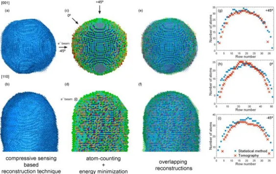
Progress in applying statistical parameter estimation theory enables us to measure unknown structure parameters with high accuracy and precision from experimental images. An overview is shown in Figure 1. This theory allowed us to measure 2D atomic column positions with a precision down to picometer scale [3, 4] or to measure the octahedral tilt in manganite heterostructures [5]. In terms of chemistry, HAADF STEM is often used. While such images are sensitive for the chemical composition, direct visual interpretation becomes inadequate whenever the difference in atomic number of distinct atomic column types is small or if the signal-to-noise ratio (SNR) is poor. To overcome this problem, statistical parameter estimation theory is used to quantify the total intensity of scattered electrons in each atomic column [6]. These intensities or so-called scattering cross sections are used to differentiate between atomic columns with different composition. Experiments on images of perovskite thin films show that columns with a difference in atomic number of only 3 can be discerned. The high chemical sensitivity of this model-based method could be further exploited to count the number of atoms with single atom sensitivity [7, 8]. By combining counting results obtained from images under different viewing directions, we have been able to reach atomic resolution in 3D which was an important milestone in the development of new electron microscopy techniques in general [7]. For heterogeneous materials, atom- counting is becoming even more challenging since small changes in atom ordering in the column have an effect on the scattering cross sections. To circumvent the need for time-consuming image simulations to compute scattering cross sections of mixed columns, an atomic lensing model is proposed based on the principles of the channelling theory. In this manner, the number of both Ag and Au atoms could be counted from an experimental HAADF STEM image of a Ag-coated Au nanorod [9]. Recently, we have shown that new possibilities emerge when combining atom-counting from a single projection image with energy minimisation to obtain a relaxed 3D reconstruction [10-12]. In Figure 2, this method is validated against state-of-the-art compressive sensing electron tomography [12]. For this purpose, three projected ADF STEM images of a Au nanorod have been acquired along different major zone axes. The close match confirms the accuracy of this new atom-counting/energy minimization approach.
[1] S. Van Aert et al., IUCrJ 3 (2016) 71.
Figure 1. (a) Locating 2D atomic columns down to picometer scale precision [4]. (b) Measurement of oxygen octahedral tilt in manganite heterostructures [5]. (c) Quantitative characterisation of an interface where the difference in atomic number between the TiO and MnO columns is only 3 [6]. (d) Counting the number of atoms in a Au nanorod with single atom sensitivity [8]. (e) 3D reconstruction of a Ag particle by combining atom counts obtained from two viewing directions [7]. (f) Number of Ag and Au atoms counted from an experimental HAADF STEM image of a Ag-coated Au nanorod [9].
Figure 2. Comparison of the atom-counting/energy minimization and atomic resolution
HRL
Electron waves for comprehensive analysis of materials properties
Hannes Lichte1, Felix Börrnert1, Bernd Einenkel1, Andreas Lenk1, Axel Lubk1, Falk Röder1, Jan Sickmann1, Sebastian Sturm1, Karin Vogel1, Daniel Wolf1
1formerly Triebenberg Laboratory*, Technische Universität Dresden, Dresden, Germany
*closed by TU Dresden by September 2016 Hannes.Lichte@Triebenberg.de
Transmission Electron Microscopy is wave optics. The object information is found both in amplitude and phase of the object exit wave. Alas, the intensity image recorded on a detector only represents the amplitude distribution whereas the phase distribution is lost. This means a substantial loss of object information, e.g. about the intrinsic electromagnetic fields in an object, which largely determine the properties.
Phases can only be measured by interference. Therefore, holography offers a powerful means for analyzing the complete electron wave including all object properties encoded in the electron phase, such as electric and magnetic fields. Due to the restrictions of electron coherence, the most powerful method up to now is off-axis image plane electron holography. It allows measuring the object phase shift on the scale reaching from several micrometers down to atomic resolution. Recent developments in Holographic Tomography give access to the 3D-distribution of electromagnetic fields.
At medium resolution with details larger than about 2 nm, the aberrations of the electron lenses can be neglected, and hence the reconstructed wave agrees with the object wave. Thus, the reconstructed phase distribution can directly be interpreted in terms of the object. This is the basis for achieving perfect phase contrast without defocusing or staining hence for determining
Mean Inner Potentials in solids
Functional potentials such as drift-diffusion potentials across pn-junctions
Electric potentials across interfaces
Trapping of charges at surfaces and interfaces
Electric potential distributions in charge-modulated structures
Magnetic fields in and around magnetic structures down to a nanoscale
Magnetic leakage fields at structural inhomogeneities
Ordering of magnetic nanoparticles
Mechanical strain
and others. All these details are significant parts of the object structure, since they determine the functionality, e.g. in semiconductors and magnetics, and hence are indispensable for a comprehensive understanding of their properties.
At atomic resolution, because of the aberrations, amplitude and phase of the reconstructed wave differ considerably from the object wave and hence cannot be interpreted directly. First, the aberrations have to be corrected by appropriate processing. Then, both in amplitude and phase, lateral resolution can be achieved as high as determined by the information limit offered by the TEM used for recording the hologram. The resulting phase images allow details of the atomic structure to be revealed, such as
Atomic potentials
Difference of atomic numbers of different constituents
by density matrices, which incorporate the propagation of coherence through the TEM.
In summary, one can say that, after 60 years of development, electron holography is an established method for comprehensive wave optical characterization of solids including their intrinsic electromagnetic fields. The performance, essentially restricted by quantum noise, allows atomic resolution both laterally and in signal. Any improvement of electron microscopes, such as of lateral resolution and of brightness of the electron gun, will enhance the capabilities of this unrivalled method for nanocharacterization.
MS 1: Functional materials and semiconductors MS1.001 invited
Interfaces in semiconductor heterostructures – requirements for quantitative, atomically-resolved STEM imaging and their intrinsic structure
A. Beyer1, K. Volz1
1Philipps-Universität Marburg, Faculty of Physics and Materials Science Center, Marburg, Germany kerstin.volz@physik.uni-marburg.de
Introduction: Modern semiconductor devices consist of several different materials, forming a heterostructure. The internal interfaces between the semiconductors often have a decisive influence on the functionality of the devices. Hence, the structure and composition of the interface are important and should be correlated to the growth conditions as well as to the optical and electrical properties of the devices. Modern STEM (Scanning Transmission Electron Microscopy) methods of course provide – especially when aberration correctors are used – the necessary atomic resolution.
Objectives: The interfaces between different semiconductors are quantified at an atomic scale with a special emphasis, which intrinsic interface structure forms depending on the properties of the semiconductor materials. To this end, polar/non-polar interface configurations are examined as well as strained and lattice-matched ones.
Moreover, the factors, which need to be taken into account when aiming for quantitative information across internal interfaces using STEM will also be discussed in this presentation.
Materials and Methods: All semiconductor heterostructures for this study are grown by metal organic vapour phase epitaxy. As an example for a lattice-matched, polar/non-polar interface GaP/Si (001) is investigated. The characteristic interface structure resulting from the charge redistribution at this interface is compared to the also lattice-matched, but non-polar interface in (Ga,In)P/GaAs (001) heterostructures.
As examples for strained interfaces Ga(P,As)/GaP as well as (Ga,In)As/GaAs interfaces are investigated.
Aberration-corrected STEM is used to characterize the interfaces at atomic resolution using a double- aberration corrected JEOL 2200 FS. Complementary frozen-phonon simulations using a highly parallelized, home-written code (STEMSalabim) are applied to derive the quantitative element depth profiles. Contrast simulations of strained in comparison to strain relaxed thin TEM specimens are also used to address the thin foil relaxation of TEM specimens, which has a significant impact on the scattered electron intensity, especially at or close to interfaces.
Kinetic as well as thermodynamic driving forces for the formation of certain interface structures are addressed by simulations using a kinetic Monte Carlo (KMC) code as well as by density functional theory (DFT).
Results: Quantitative atomic resolution in STEM imaging can be achieved when the experimental images are compared to frozen phonon simulations, which take the geometric aberrations as well as the source size and distribution of the microscope used into account. The agreement between simulation and experiment can be optimized when also the amorphous layers, generated at the top and bottom of the
interfaces can be tackled using aberration-corrected STEM imaging and complementary contrast simulation. The factors, which need to be taken into account when contrast simulations are performed will be discussed as well as several examples of intrinsic interface structures in semiconductor heteroepitaxy will be given and correlated to the optoelectronic excitations across those interfaces.
We gratefully acknowledge support of the German Science Foundation (DFG) in the framework of the SFB 1083 Structure and Dynamics of Internal Interfaces.
MS1.002 invited
EELS and nanoCL for probing electronic and optical defect-induced phenomena in functional
L. H. G. Tizei1, A. Gloter1, M. Kociak1, A. Zobelli1, G. Tieri1, O. Stéphan1
1Université Paris-Sud, Laboratoire de Physique des Solides, Orsay, France odile.stephan@u-psud.fr
The field of electron scanning transmission electron microscopy (STEM) has recently achieved a succession of impressive successes linked with the development of aberration correctors, enabling atomically-resolved spectroscopy and new imaging modes, which are spreading worldwide. The development of Electron Energy-Loss Spectroscopy (EELS) detectors with single electron sensitivity offers new opportunities for collecting EELS spectra with enough signal to noise ratio to evaluate doping and chemical changes at the order of a few percents while keeping an atomic resolution. Similarly, recent progress in the collection of visible-range photons emitted by a sample illuminated by a focused beam has enabled novel cathodo-luminescence (CL) experiments in a STEM for exploring the optical (emission) properties of materials down to the nanometer scale and ultimately for entering the field of quantum nano-optics [1]. Combining these multiple investigation channels is of particular relevance for investigating and tuning the role of defects such as atomic dopants, stacking faults or interfaces on the properties of functional materials. Some examples such as interface driven effects in oxide heterostructures or the intimate link between structural defects and optical properties of 2D semiconducting materials will be reviewed. This includes a discussion on:
- the relation between the electronic charge distribution and interface reconstruction in manganite- nickelate [2] or manganite-ferroelectric [3] heterostructures,
- the interplay between Cr dopants and vacancy clustering in the structural and optical properties of WSe2 [4],
- stacking order effects on near band edge excitons in h-BN [5],
- the identification of point defects in h-BN as bright UV single photon emitters [6].
[1] L. H. G. Tizei and M. Kociak, Spectrally and spatially resolved cathodoluminescence of nanodiamonds: local variations of the NV0 emission properties, Nanotechnology 23, 175702 (2012) [2] Gibert et al., Interfacial Control of Magnetic Properties at LMO/LNO Interfaces, Nano letters 15, 7355
(2015)
[3] Marinova et al., Depth profiling charge accumulation from a ferroelectric into a doped Mott insulator, Nano letters 15, 2533 (2015)
[4] L. H. G. Tizei, unpublished results
[5] R. Bourrelier et al., Nanometric Resolved Luminescence in h-BN Flakes: Excitons and Stacking Order, ACS Photonics 1, 857 (2014)
[6] Romain Bourrellier et al., Bright UV Single Photon Emission at Point Defects in h-BN, Nano Lett., 16, 4317 (2016)
Energy-filtered TEM studies on silicon nanoparticles acting as quantum dots in single electron transistors
D. Wolf1,2, X. Xu1, T. Prüfer1, G. Hlawacek1, L. Bischoff1, W. Möller1, H. J. Engelmann1, S. Facsko1 J. von Borany1, K. H. Heinig1, R. Hübner1
1Helmholtz-Zentrum Dresden-Rossendorf, Institute of Ion Beam Physics and Materials Research, Dresden, Germany
2Leibniz Institute for Solid State and Materials Research, Dresden, Germany d.wolf@hzdr.de
The miniaturization of computing devices and the introduction of the internet of things generate an increasing demand for the development of low-power devices. Single electron transistors (SETs) are ideally suited for this demand, because they are promising very low power dissipation devices. For room- temperature operation of an SET it is necessary to create a single quantum dot (QD) with a diameter below 5 nm exactly positioned between source and drain at a tunnel distance of only a few nanometers.
Within the IONS4SET project [1], we aim to achieve this goal by ion irradiation induced Si-SiO2 mixing and subsequent thermally activated self-assembly of single Si nanocrystals surrounded by a thin SiO2
layer. This process is illustrated in Fig. 1 by means of simulations results.
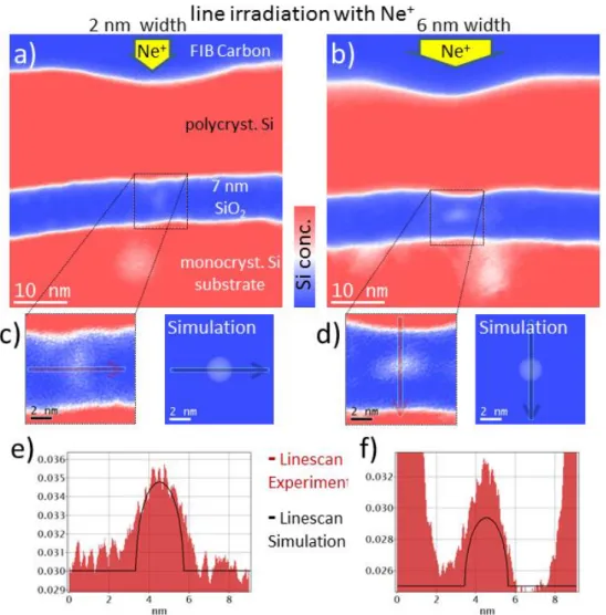
Here, we present energy-filtered (EF)TEM studies in order to monitor the influence of process parameters, such as stack geometry, ion fluence for irradiation, annealing temperature and annealing time, on the self-assembly of Si QDs. Fig. 2 shows representative EFTEM micrographs of a Si-SiO2-Si layer stack imaged using different electron energy-loss (EEL) windows. The Si plasmon-loss filtered images yield thereby the best signal-to-noise for detection of Si nanodots, because the Si plasmon peak is the most intense peak with a relatively small FWHM of 4 eV in the EEL spectrum.
Moreover, since the obtained (raw) EFTEM images provide only qualitative information about the Si concentration in the oxide layer, they cannot give a clear answer if for example the observed contrast corresponds to one or more Si nanodots (NDs) in projection. Therefore, EFTEM images are quantified further by converting them into so-called thickness over mean free path length (MFPL) t/λSi maps, in which λSi is the MFPL corresponding to the chosen energy range. The experimental t/λSi maps are then compared with simulated t/λSi maps of a single Si ND. Fig. 3 depicts that our approach enables us not only to detect single Si nanodots (Fig. 3c,e) but also to count them if they are arranged in projection direction of the electron beam (Fig. 3d,f). For these experiments, the layer stacks were irradiated with Ne+ ions within an Orion NanoFab (Zeiss). This allows controlled line or point irradiation and ensures Si QD formation within a confined region. In a next step, confined regions will be established by fabricated nanopillars that enhances reproducibility as the volume relevant for the self-assembly of the nanocluster will be better defined.
[1] We thank for financial support within the European Union"s Horizon 2020 research and innovation program under Grant Agreement No 688072 (Project IONS4SET).
Figure 2. EFTEM imaging of a Si-SiO2-Si layer stack broad-beam irradiated with 30 keV Si+ ions. The images are taken at 0 eV, 17 eV, and 25 eV using 5 eV, 7 eV, and 5 eV slit widths for the zero-loss, Si plasmon-loss, and SiO2 plasmon-loss images, respectively. The 2-3nm small Si nanodots can only by observed as bright (dark) contrast in the Si (SiO2) plasmon-loss, whereas in the zero-loss image they are not visible.
Figure 3. EFTEM imaging of a Si-SiO2-Si layer stack line-irradiated with 30 keV Ne+ ions. a,b)
Experimental thickness over MFPL (t/λSi) map gained from a Si plasmon-loss TEM image. c,d) Inset of the Si QD and its simulated t/λSi map. e,f) Line profiles along the line scans in (c) and (d) suggest that there is a single ND in (e) and there are two NDs in projection in (f).
MS1.004
Morphology of InAs/InAlGaAs quantum dots emitting in the low-loss telecom wavelength ran
M. Schowalter1,2, C. Carmesin3, M. Lorke3, D. Mourad3, T. Grieb1,2, K. Müller-Caspary4, M. Yacob5 J. P. Reithmaier5, M. Benyoucef5, A. Rosenauer1,2, F. Jahnke3
1Universität Bremen, Institut für Festkörperphysik, Bremen, Germany
2Universität Bremen, Mapex center for materials and processes, Bremen, Germany
3Universität Bremen, Institut für Theoretische Physik, Bremen, Germany
4University Antwerp, EMAT, Antwerp, Belgium
5Universität Kassel, Institut für Nanostrukturtechnologie und Analytik (INA), Kassel, Germany schowalter@ifp.uni-bremen.de
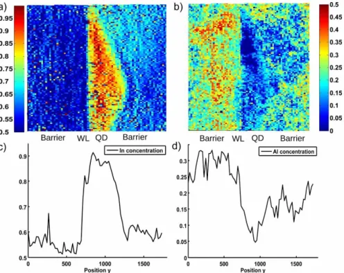
Among the main challenges for quantum information technology is the realization of deterministic single photon sources with emission energies in the low-loss telecom band [1]. InAs/InAlGaAs/InP is a promising material system, since it allows growth of quantum dots that emit within this energy range [2, 3]. To achieve a deeper understanding of the emission properties, a detailed characterization of the morphology of the quantum dots including composition determination within the dots is necessary. In this contribution we developed a technique for the composition quantification in this quaternary alloy based on quantitative STEM. Measured composition and morphology were then used in atomistic tight-binding simulations to model the inhomogeneous broadening of the photoluminescence of the dot ensemble.
Fig. 1a shows an overview of the structure exhibiting the top of the InP/InAlGaAs DBR structure on which the InAs/InAlGaAs active region was grown. An overview of the active region (Fig. 1b) shows that the quantum dots exhibit a pyramidal shape with (1-13) side facets. A higher intensity (Figs. 1c, d) on top of their side facets is observed that hint on a diffusion of In out of the dot towards the cap layer.
To quantify the composition within the dots quantitative STEM as outlined in [4] was employed. However, since the barrier consists of a quaternary material, an intermixing of the metals is possible and the method of [4] needs to be extended. For that purpose, Reference: data of HAADF intensity and strain (Fig. 2 a, b) were simulated as a function of thickness, In and Al concentration. Isolines of strain and intensity in these data exhibit an angle of 45° and therefore the two quantities are sufficiently independent to be used for quaternary composition quantification. Strain and intensity were measured from HRSTEM images and then compared with the Reference: data set to determine both compositions.
Fig. 3 a-d show In and Al concentration distributions within a quantum dot as well as composition profiles through the center of the dot. Both composition distributions exhibit the pyramidal shape of the quantum dot. Regions on top of the side facets (with increased intensity in fig. 1 c and d) exhibit a slightly larger In concentration as well as a slightly reduced Al concentration. The In concentration profile increases to a constant value of about 86 %, whereas the Al concentration drops towards about 7 % suggesting equal Al and Ga concentration. Since the pyramidal quantum dot is embedded in the InAlGaAs matrix, the true concentration within the dot must be increasing linearly from bottom to top.
For further atomistic-tight binding simulations, the pyramidal shape as well as the linearly increasing In concentration within the dot were adopted. Simulations were carried out as a function of the size of the pyramid base from 40 – 60 nm with constant diameter to height ratio and as a function of In concentration at the base of the pyramid from 70 to 100 % (assuming an equal distribution of the remaining lattice sites by Al and Ga atoms). Only a shift of about 20 meV due to the size, but a shift of
Figure 1. a) STEM overview image of the sample. b) STEM image of the active region. c) and d) HAADF STEM images of two quantum dots.
Figure 2. a) Simulated HAADF STEM intensity and b) strain as a function of In and Al concentration.
Figure 3. a) and b) In and Al concentration maps of a quantum dot. c) and d) Respective concentration profiles through the middle of the dot.
Anisotropic polarization in a Bi0.8Ca0.2FeO3 thin film investigated by combined HAADF/ABF imaging
M. Campanini1, R. Erni1, M. D. Rossell1
1EMPA, Dübendorf, Switzerland marco.campanini@empa.ch
In the last decade BiFeO3 (BFO) has been widely investigated for being one of the few multiferroic materials that exhibits ferroelectricity and ferromagnetism at room temperature. Despite the G-type antiferromagnetic ordering, the arrangement of spins in a cycloidal structure along the [110] direction of the R3c structure of BFO suppresses its macroscopic magnetization; nevertheless, it has been proven that this spiral spin structure can be destroyed by Ca doping, obtaining a canted antiferromagnetic structure which is weakly ferromagnetic.1
In order to preserve an overall charge neutrality in Bi1-xCaxFeO3, alongside with the Ca substitution on perovskite A sites, oxygen vacancies are spontaneously produced and structures with oxygen-vacancies ordering have been commonly reported in a range of doping of 0.2<x<0.5.2
Although the macroscopic effects of doping on the magnetoelectric properties of bulk BFO have been extensively investigated, the detailed atomic configuration in these doped materials and a direct correlation between the structure and their properties at a very local scale is still missing. More recently high-quality epitaxial single crystal BFO thin films have been fabricated and they represent the best candidates to address unresolved questions about this intriguing material.
In this work, high angle annular dark-field (HAADF) and annular bright-field (ABF) imaging performed in aberration-corrected scanning transmission electron microscopy (STEM) were employed to elucidate the mechanism of doping/O-vacancy ordering in a Bi0.8Ca0.2FeO3 thin film and to correlate its polarization to the atomic scale structure.
A single-crystalline 85 nm thick Bi0.8Ca0.2FeO3 film was grown on (001) SrTiO3 substrate, using pulsed laser deposition.
We have employed HAADF to map the Ca doping while ABF was successfully used to visualize O distribution and O vacancies ordering. The fitting of the peaks in the HAADF/ABF images, carried out using a modified version of the algorithm proposed by Yankovich3, permits to directly access the projected crystallographic structure and to make quantitative analysis.
The polarization maps and other structural distortions were calculated from the precise position of the atomic columns in the structure.
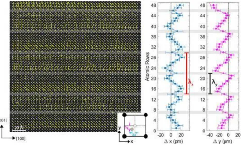
The investigated Bi0.8Ca0.2FeO3 thin film displays a regular arrangement of O vacancies in a periodic superstructure, superimposed to a doping gradient in between the layers (Fig.1).
The atomic configuration of the layers containing ordered O vacancies was obtained analyzing HAADF and ABF intensities, while the coupling between different polar and non-polar distortion is explained by direct structural imaging along different crystallographic orientations.
By mapping the polarization at the atomic scale, we observed the establishing of a periodic ferroelectric distortion with an anisotropic nature, displaying two different periodicities along the [001] and [100]
perovskite directions (Fig.2).
Remarkably, we show that this anisotropic polarization is strictly related to the Ca doping gradient, which is able to actively alter the ordering of the lone pair of Bi atoms.
A direct correlation between the structure of the doped material and the polarization has been pointed out at atomic scale thanks to quantitative HAADF/ABF analysis.
The presented findings highlight the relevance of anisotropic doping for advanced multiferroic materials engineering, representing an additional degree of freedom that can be exploited –together with the epitaxial strain–4 to tailor the properties and control the coupling between different ferroic orderings in magnetoelectric thin films5.
Figure 1. Ordering of O vacancies and structure of the defective layers in Bi0.8Ca0.2FeO3.
Figure 2. Polarization map and Fe atomic displacements due to the lone pair ordering on Bi sites.
Quantitative characterization of nanosized conducting filaments formed by atomic-scale defects in redox-based resistive switching memories
H. Du1,2, C.-L. Jia1,3,4, A. Koehl3, J. Barthel1,2, R.Dittmann3, R. Waser3,5,6, J. Mayer1,2,6
1Forschungszentrum Jülich GmbH, Ernst Ruska-Centrum für Mikroskopie und Spektroskopie mit Elektronen, Juelich, Germany
2RWTH Aachen University, Gemeinschaftslabor für Elektronenmikroskopie, Aachen, Germany 3Forschungszentrum Jülich GmbH, Peter Grünberg Institute, Jülich, Germany
4Xi’an Jiaotong University, School of Electronic and Information Engineering, Xi'an, China 5RWTH Aachen University, Institut für Werkstoffe der Elektrotechnik II (IWE II), Aachen, Germany 6Jülich-Aachen Research Alliance, Future Information Technology (JARA-FIT), Jülich-Aachen , Germany jen@pdi-berlin.de
Introduction: Redox-based resistive switching phenomena are found in many metal oxides and hold great promise for applications in next-generation memories and neuromorphic computing systems. Resistive switching involves the formation and disruption of electrically conducting filaments through ion migration accompanied by local electrochemical redox reactions. These structural changes are often explained by point defects, but so far clear experimental evidence of such defects is missing.
Objectives: In this work [1], we apply STEM, EELS and EDX imaging techniques to quantitatively characterize nanosized conducting filaments in electroformed Au/FeSrTiO3/Nb:SrTiO3 thin film devices, providing direct experimental evidence for the point defect nature of the conducting filaments.
Materials and Methods: SrTi0.98Fe0.02O3 thin films about 17 nm in thickness were expitaxially grown on a 0.5-wt% Nb doped SrTiO3 substrate by PLD. Electric forming was performed on individual devices by a sweep to 5 V setting the devices into the ON state. Cross-sectional TEM specimens were cut by FIB and further thinned by Ar-ion beam milling. STEM and EDX spectrum imaging was conducted with an FEI ChemiSTEM microscope at 200kV. Monochromated EELS spectrum imaging was performed with the FEI PICO microscope at 200 kV with spectrum energy resolution of 0.2–0.3 eV. Image simulations were performed with the Dr. Probe software package.
Results: In both ABF and HAADF images, we observed V-shaped areas showing darker contrast in the compared with their surroundings (Fig. 1). This provides a first indication that these areas are conducting filaments viewed in cross-section.
A Ti3 distribution map was obtained by monochromated EELS spectrum imaging (Fig. 2), which clearly reveals four different V-shaped defect areas in the film developed to different stages of completion from the top anode towards the cathode i.e. he conducting substrate. The shape of the filaments can be explained by the electric field and chemical gradients around the filaments driving ion drift and chemical diffusion, respectively.
Quantitative EDX analysis indicates also considerable Sr- and O-vacancies in the filaments. By taking both Sr-deficiency and static lattice distortion into account, multislice STEM image simulations can qualitatively reproduce the decrease of mean intensity in both ABF and HAADF images of the filaments.
Intriguingly, atomic resolution STEM imaging reveals that the perovskite lattice is maintained intact at such high defect concentrations and considerable lattice distortions (Fig. 3).
Conclusion: The present work [1], for the first time, provides clear experimental evidence for the existence of multiple nanosized conducting filaments formed solely by atomic-scale point defects in a SrTiO3 based thin film device. First insights into the switching mechanism are deduced from a snapshot simultaneously showing multiple nanosized filaments in different evolutionary stages. The coexistence of a high Ti3 concentration along with Sr- and O-vacancies in the conducting filaments, provides atomic scale explanations for the resistive switching mechanisms. The results shed unique light on the complexity of the conducting filaments formation that cation and anion defects need to be considered jointly.
Figure 1. a) Schematic of an electroformed ON-state Au/Fe:SrTiO3/Nb:SrTiO3 device. b) I-V curve of the electroforming process. Overview HAADF c) and ABF d) STEM images of the device cross-section, arrows indicate the film/substrate interface.
Figure 3. a) ABF image of the region marked in Fig 1d. Lines denote the film/substrate interface. b) Magnified part marked in a). c) Corresponding HAADF image to b). Atomic symbol Sr: green, Ti: red, O:
blue.
MS1.P001
Structural properties of Fe3Si/Ge/Fe3Si thin film stacks on GaAs
B. Jenichen1, S. Gaucher1, J. Herfort1, U. Jahn1, H. Kirmse2, M. Hanke1, A. Trampert1
1PDI, Berlin, Germany
2HUB, Berlin, Germany jen@pdi-berlin.de
Introduction: A high structural quality of ferromagnet/semiconductor/ferromagnet (FM/SC/FM) thin film systems can be achieved by reducing the mismatch of the lattice parameters of the films. Following this rule Fe3Si/Ge/Fe3Si thin-film stacks were fabricated on GaAs(001) using molecular beam epitaxy (MBE).[1] Lattice matched Co2FeSi/Ge/Co2FeSi tri-layer stacks were grown on Ge(111) as well.[2]
Objectives: On the GaAs(001) substrates the quality of the Ge layer between the two Fe3Si films had to be improved, because the direct growth of a semiconductor film on a metal still remains difficult.
Therefore, in the present work we realize highly perfect epitaxial films using solid phase epitaxy (SPE).[3]
Materials and Methods: The Fe3Si/Ge/Fe3Si films prepared by MBE and SPE were characterized by high-resolution transmission electron microscopy (TEM), reflection high-energy electron diffraction (in- situ during annealing), energy dispersive x-ray spectroscopy (EDX) in the TEM, electron backscattered diffraction (EBSD) and x-ray diffraction (XRD).
Results: All the films show a high structural quality over large areas as evidenced by TEM, EBSD and XRD. EBSD reveals only one single orientation of the top Fe3Si film and at the same time the image quality is very high. We find evidence for a spontaneously formed vertical superstructure in the Ge film (Fig.1,2). The XRD curves exhibit superstructure maxima caused by the ordered regions as well as clear thickness fringes resulting in interference patterns. We find evidence for the diffusion of silicon and iron into the Ge film, i.e. the semiconductor layer is not pure Ge but a mixed crystal consisting of Ge with Fe and Si. This film is no longer fully lattice matched with the GaAs substrate but tetragonally strained without plastic relaxation. XRD curves were simulated assuming a FeSi/Ge superlattice for the Ge(Fe,Si) film in correspondence with the EDX results.
Conclusion: The SPE approach is therefore a suitable tool to explore the combination of ferromagnetic Heusler alloys with semicondoctors in FM/SC/FM systems, a step towards the implementation of new vertical spintronics devices.
References:
[1] B. Jenichen et al., Thin Solid Fims, 556, 120 (2014) [2] M. Kawano et al., J. Appl. Phys. , 119, 045302 (2016), [3] S. Gaucher et al. Appl. Phys. Lett., accepted for publication.
Figure 1. TEM micrograph of a Fe3Si/Ge/Fe3Si thin-film stack, the superstructure region in the Ge layer is clearly visible.
Figure 2. SAD pattern of the sample imaged in Fig. 1 (contrast inverted).
MS1.P002
In situ TEM of the transformation fatigue of TiNi based shape memory alloys
T. Wuttke1, C. A. Volkert1
1University of Göttingen, Institute of Materials Physics, Göttingen, Germany twuttke@gwdg.de
Introduction: Shape Memory Alloys (SMAs) are named after their ability to recover plastic deformation upon heating. The key mechanism responsible for this behavior is a reversible diffusionless solid-state phase transition between a highly twinned martensitic state and an untwinned austenitic phase [1]. This allows to use SMAs as actuators in various industrial, scientific and medical fields [2, 3].
A big drawback for many SMAs is the so called transformation fatigue. This term describes the cumulative increase of irreversible plastic deformationduring thermal or mechanical cycling which results in a limited lifetime of the SMA [4].
Objectives: Our goal was to study the change in microstructure of TiNi based SMAs during thermal cycling using in-situ TEM techniques.
Materials and Methods: Both Ti51Ni49 and Ti50Ni30Cu20 alloys were prepared with vacuum arc melting.
Binary TiNi alloys are known to be strongly affected by transformation fatigue while the addition of copper increases the lifetime [5]. TEM specimens were prepared with a combination of ion polishing and FIB.
Experiments have been carried out using a Gatan heating holder and a Nanofactory STM-holder. The later features a moveable tungsten tip on a piezo actuator, mounted opposite to the specimen. Voltage application between tip and specimen allows to rapidly cycle the temperature several hundred times in a few minutes using Joule heating.
Results: Figure 2 shows the microstructural development of a Ti51Ni49 alloy over the course of 200 thermal cycles. Since each image shows the sample at room temperature, there should be no changes in case of a perfectly reversible phase transformation.
Three observations can be made. First, the amount of well ordered twinned martensite decreases with increasing cycle count. The term ordered martensite refers to the nicely twinned microstructure of a single martensite variant in contrast to the chaotic microstructure of several competing variants. Second, the total amount of martensite also decreases. This is partly due to thermal drift but mostly due to a movement of the interface in favor of the austenite. Third, defects appear at the austenite-martensite interface. Interestingly, these changes are not strictly irreversible but are occasionally undone during later cycles, as one can see when comparing cycle 48 and 73 in figure 2. In average, the amount of ordered martensite decreases nevertheless, as is shown in figure 3.
Similar experiments were carried out with Ti50Ni30Cu20 samples for which no microstructural changes have been observed.
Conclusion: In case of Ti51Ni49 the formation of martensite becomes more and more difficult with increasing cycle count. This hints at the formation of defects which hinder the movement of the interface.
Martensite nucleation has a stochastic element which might explain why the formed martensite occasionally appears in a less chaotic microstructure compared to earlier cycles.
Ti50Ni30Cu20 is known for its increased lifetime and therefore serves as a control experiment where microstructural changes were neither expected nor observed.
Figure 1. Microstructural changes of a TiNi alloy during thermal cycling. Shown is the sample in the cold state after a certain amount of transformation cycles have been carried out.
Figure 2. Thermal cycling of a TiNi alloy. Shown is the running average of the area fraction of ordered martensite in relation to the initial state.