Local tunneling decay length and Kelvin probe force spectroscopy
Florian Albrecht,1,*Martin Fleischmann,2Manfred Scheer,2Leo Gross,3and Jascha Repp1
1Institute of Experimental and Applied Physics, University of Regensburg, 93053 Regensburg, Germany
2Institute of Inorganic Chemistry, University of Regensburg, 93053 Regensburg, Germany
3IBM Research–Zurich, 8803 R¨uschlikon, Switzerland (Received 19 October 2015; published 28 December 2015)
In the past, current-distance spectroscopy has been widely applied to determine variations of the work function at surfaces. While for homogeneous sample areas this technique is commonly accepted to yield at least qualitative results, its applicability to atomic-scale variations has not been proven neither right nor wrong. Here we benchmark measurements of the current-distance decay constant against the well established Kelvin probe force spectroscopy for four distinctly different cases with atomic-scale variations of the local contact potential. The two techniques yield quite different results. Whereas the maps of the current-distance decay constant are consistent with being topographical artifacts, the Kelvin probe force spectroscopy maps show variations of the local contact potential difference in agreement with expected surface dipoles. This comparison clarifies that maps of the current-distance decay constant are not suited to directly characterize contact potential variations at surfaces on atomic length scales.
DOI:10.1103/PhysRevB.92.235443 PACS number(s): 68.37.−d,68.43.−h,68.37.Ef I. INTRODUCTION
Since the early days of scanning tunneling microscopy, current-distance [I(z) - withIbeing the tunneling current and z the tip sample spacing] spectroscopy has been applied to determine variations of the work function at surfaces [1,2]. In the one-dimensional description of quantum tunneling through a rectangular barrier, the transmission probability decays exponentially with the barrier’s thickness, with the decay length being inversely proportional to the root of the barrier height [3]. Consequently, one expects that from the decay length determined from current-distance spectra the barrier height can be extracted, which—in simplest approximation—
is the mean of the work function of the tip and the sample.
It has been early realized that several corrections are needed, because of the tunneling junction being three-dimensional in nature [4–6], the applied bias voltage [7–9] or image charge effects [10] altering the barrier’s shape, for example. In this context a so-called effective barrier height has been introduced, to still make use of the simple description. But despite such corrections, one still may expect a well-defined and monotonic relationship between the inverse of the decay length and the local work function of the sample for a given tip.
For extended, homogeneous samples, the above described relationship seems to hold and the decay length is assumed to provide at least some qualitative trends of the surface contact potential [5,11,12]. However, for strongly corrugated samples, from very basic arguments, one can show that the geometry will affect I(z) spectra [5,13,14] even if the work function is assumed to be constant over the sample, as will be discussed further below. In the past, maps of the current-distance decay constant on molecular and submolecular length scales have been extracted and interpreted in various aspects [15–20].
However, it has never been rigorously tested, as to whether or not the current-distance decay length carries reliable
*florian.albrecht@ur.de
information of local surface dipoles or variations of the contact potential on the very local scale.
Hence, benchmarking the technique is in order. Kelvin probe force spectroscopy (KPFS) [21] is an established technique to reliably extract variations of the contact potential on the very local scale [22–30]—at least as long as the tip is far enough from the sample and not entering the regime of Pauli repulsion [31,32]. Further improvements of the interpretation and data acquisition of KPFS and related techniques are active fields of research, progressing fast at the moment [33–37]. KPFS is based on atomic force microscopy, where the minimization of the electrostatic interaction as a function of bias voltage yields the voltage of compensated contact potential difference between the tip and the sample.
As scanning tunneling microscopy (STM) and atomic force microscopy (AFM) can be combined in a single apparatus making use of the very same tip, the benchmarking can be done under identical conditions of the tip-sample junction. Another STM-derived technique, which can be used to detect variations of the contact potential difference, is based on measuring field emission resonances [38,39]. However, this is not expected to work at a (sub)-nanometer length scale, since the lateral confinement would affect the energies of the resonances [38].
Apart from the above-mentioned possible geometry-related artifacts, there are quite a few other problems associated with extracting effective barrier heights fromI(z) spectra. At the technical side, a finite impedance of the bias voltage supply or the current preamplifier input may effect the apparent decay length [40], for example. As rather fundamental issues we would like to mention mechanical deformations of the tip- sample junctions close to the contact point [40,41] and band bending effects in a semiconductor sample, the latter resulting in a complete failure of this technique [42].
The issues mentioned in the previous paragraph are not subject of this study. Instead, we investigate the reliability of detecting surface contact potential variations at atomic length scales from I(z) spectroscopy. To this end, we benchmark maps of tunneling decay length derived from I(z) spec- tra against maps of voltages of compensated local contact
potential difference (VCPD) from KPFS for test cases which show tunneling current variations on the very local scale.
II. METHODS
Experiments were performed using a homebuilt qPlus- based [43] frequency-modulated atomic force microscope [44]
in ultrahigh vacuum (p ≈ 5×10⁻¹¹mbar) at low tem- peratures of ≈5 K including scanning-tunneling functional- ity. All investigations of trimeric ortho-phenylene mercury (H12C18Hg3) [45], trimeric perfluoro-ortho-phenylene mer- cury (F12C18Hg3) [46], and perylene-3,4,9,10-tetracarboxylic dianhydride (PTCDA) were performed with the molecules directly adsorbed on Cu(111), whereas 10-chloro-anthracene- 9-carbonitrile (ClAnCN) was studied on a double layer of NaCl on Cu(111). All these molecules and Au atoms were deposited onto the cold sample (T <15 K) with the sample being located inside the STM/AFM. Except for the data on the Au adatoms on NaCl, the tip was functionalized with a CO molecule [26,47], and bias voltages refer to the sample with respect to the tip. All KPFS data were obtained at a 0.5 ˚A oscillation amplitude. During the acquisition of an entire data set providing a map of VCPD and current decay length, the feedback loop was switched off. Specifically, also while moving the tip from one to another of the grid points, the feedback loop was never switched on. This is important to ensure that local variations of the tunneling current cannot influence the spectra indirectly via vertical displacements of the tip. The tip sample spacing is estimated from AFM data for CO functionalized tips and given in terms of center-to-center distance of the last tip atom the top-most metal layer of the sample [32]. In case of the Au adatoms on NaCl the tip sample spacing refers to the STM point contact between tip and metal sample.
III. PRELIMINARY CONSIDERATIONS
In the following it will be discussed, how a strong corru- gation of a sample with a homogeneous contact potential may affect the decay length inI(z) spectra. To picturize that, we assume to have a fictitious local corrugation of the sample that should have a completely homogeneous contact potential, that is, for this thought experiment we disregard the Smoluchowski effect [48]. The larger the average tip-sample distance, the more any local corrugation of the sample will become laterally washed out in STM images for simple geometric reasons.
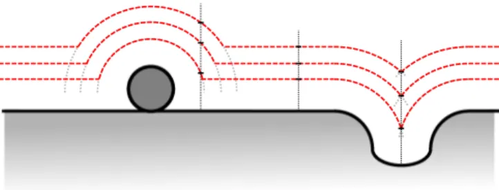
Figure1schematically depicts this situation by showing line profiles of constant current for different set point values as a cross section through the sample. In a very simple picture, one may assume that the constant-current isosurfaces around an adatom are concentric spheres around it. Hence, with decreasing current set point, the radius of the respective sphere increases and thus also the lateral extent of the protrusion in the image. From this simple geometric effect described above, it follows that the line contours will become more sparse just next to a local corrugation of the sample, resulting in an apparent increase of the current decay length [5,13,14], even though in this thought experiment the contact potential was homogeneous. Analogous arguments apply for sharp step edges.
FIG. 1. (Color online) Illustration how the local topography can influence the apparent tunneling current decay length. If one assumes that profiles of constant current (dashed lines) follow the topography at different distances, beside protrusions and in trenches the line contours will become more sparse as compared to the flat terraces (see vertical dotted lines).
IV. CHOICE OF SYSTEMS
After considering the above, one wants to benchmark the technique for cases, in which the constant-current profiles show local corrugation and the local contact potential is expected to vary over the sample. Here we chose several distinctly different test cases, which are briefly introduced in the following. As almost pointlike surface dipoles altering the local contact potential we investigated individual Au adatoms on top of a bilayer of NaCl on Cu(111). These are associated with a protrusion in constant-current topography images with a large apparent height. They can be deliberately charged negatively [49], giving rise to a change in the KPFS signal [25]. Further, we used several molecular systems for benchmarking, the KPFS data of which we published recently in a different context [32]. One of these molecular systems is PTCDA adsorbed on Cu(111), which is known to reduce the work function of Cu(111) [50,51]. Due to the charge transfer inside the molecule [52] as well as between the substrate and the molecule, this molecule represents an overall surface dipole rather delocalized over the entire molecule. A different situation arises for ClAnCN molecules, in which the chlorine and the carbonitirile moieties carry different partial charge giving rise to an in-plane dipole of the molecule. This molecule was studied on top of a NaCl bilayer to also test a distinctly different current regime. Finally we investigated trimeric perfluoro-ortho-phenylene mercury (F12C18Hg3) and its hydrogen-terminated counterpart H12C18Hg3. This direct comparison of molecules with fluorine versus hydrogen termination enables having different surface dipoles and local contact potentials while keeping an almost identical geometry.
On top, these molecules exhibit a pronounced and rather sharp dip in their constant-current profile directly inside the molecule. This renders this an appropriate test case for artifacts arising from sharp features in constant-current profiles as they are discussed in the previous section.
V. DATA ACQUISITION
We acquired KPFS maps of the local contact potential difference along with maps of the inverse current decay length.
To this end, for each lateral position on a dense grid a KPFS parabolaf(V) at a safe distance to avoid artifacts [32] and twoI(z) curves at different voltages are recorded immediately
(a)
-0.2 0 0.2 0.4
-3 -2
bias [V]
∆f [Hz]
10.0 10.5 11.0 11.5 1
10
tip height [Å]
I [pA]
VCPD
(b)
FIG. 2. (Color online) Exemplary curves of KPFS andI(z) mea- surements. (a) KPFS parabola: raw data (blue) along with parabolic fit (red). The maximum position of the parabola gives the local VCPD value (green). (b) Logarithmic plot ofI(z) curves at different bias voltages: raw data (blue) along with exponential fits (red).
one after another. Figure2shows exemplarily a set of these curves. Each of the f(V) and I(z) spectra is fitted to a parabolaf(V)=f+a(V −VCPD)2 and an exponential decay I(z)=I0exp(−2κz), respectively. Here, f and a denote the maximum value of the parabolic fit and its curvature, respectively.VCPDcorresponds to the voltage of compensated contact potential difference (VCPD).I0is a constant prefactor for the exponential current fit. Out of the fitting parameters f,a,VCPD,I0, andκ, relevant in the present context are the VCPD and the inverse of the current decay length 2κ.
VI. RESULTS
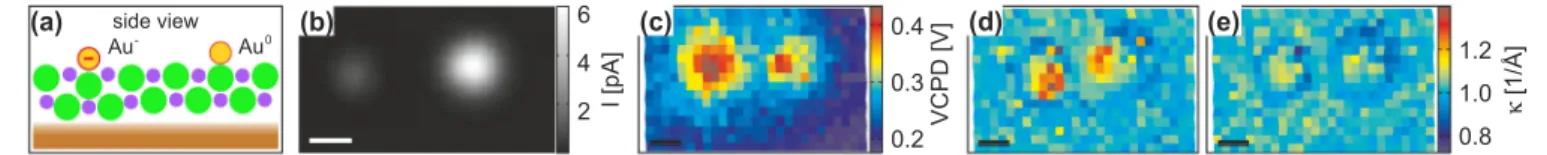
We start with the discussion of deliberately charged individual Au adatoms on a bilayer of NaCl on a Cu(111) surface [49]. The corresponding data were recorded with a metal tip. To examine the effect of a localized charge we investigated two adatoms next to each other, where one of them was prepared in the anionic state [49], as depicted in a cross sectional drawing in Fig.3(a). The appearance of the two species in STM images [Fig.3(b)] is different in accordance with previous results [25,49]. The VCPD map [Fig. 3(c)]
shows a significant increase above the anion as is expected and reported before [25]. Interestingly, the VCPD values are also increased above the neutral Au atom, which we ascribe to a weak but slightly polar bond between the Au adatom and the Cl ion below or to polarization effects. However, the feature of increased VCPD is distinctly smaller in the lateral direction in the case of the neutral Au atom as compared to the anion. Inκmaps, see Figs.3(d)and3(e), the two species are indistinguishable from each other within the noise floor of the experiment. Theκmaps acquired at negative and positive bias voltages of 0.5 V show a clear difference with respect to each other and with respect to the VCPD map. In particular theκ map acquired at positive bias voltage, displayed in Fig.3(e), exhibits rings of decreasedκaround the adsorbates as primary
features. These features are exactly what can be expected from simple geometry considerations as artifacts; see above (Fig.1).
Also the diameters of these rings in theκ map correspond to the lateral sizes of gold adatoms in the tunneling current image [Fig.3(b)], supporting the assignment as topographic artifacts.
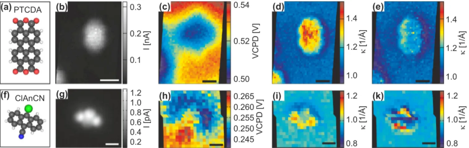
Next we turn to PTCDA on clean Cu(111) and ClAnCN on bilayer NaCl on Cu(111), the data sets of which were recorded with CO functionalized tips. The structures of those molecules are depicted in Figs. 4(a) and 4(f), respectively, their constant-height STM images in Figs. 4(b) and 4(g), respectively. As is discussed above, for PTCDA on copper, one expects an overall surface dipole distributed over the entire molecule, arising from the interaction between the molecule and the substrate [50,51]. The dipole is expected to reduce the VCPD above the position of the molecule. Figure 4(c) showing the VCPD map is in very good agreement to that.
In contrast, theκ map recorded at negative bias [Fig. 4(d)]
shows even an increase ofκvalues above the molecule, which would indicate an increase of the work function. Theκ map recorded at positive bias also shows increased values above the molecule, although much less pronounced. Here a halo of κ values decreased with respect to the substrate around the molecule becomes apparent—as in the case of gold adatoms.
For the ClAnCN molecule the VCPD map [Fig.4(h)] shows a reduction in the work function above the position of the chlorine atom and an increase above the carbonitrile group.
Theκmap recorded at negative bias voltage [Fig.4(i)] shows contrast in rough agreement with the VCPD map; however, yet again theκ maps acquired at negative and positive bias voltages are quite different.
Finally, the results obtained on the two organometallic molecules F12C18Hg3and H12C18Hg3are presented in Fig.5, starting with their structure shown in panel (a). Figure5(b) shows the constant-height STM image of the two molecules investigated right next to each other in the same data set with the very same tip. Important for the discussion of theκ maps is the observation that the STM images are very similar for the two cases and that the STM images of both molecules exhibit distinct trenches. The VCPD map [Fig. 5(c)] shows the expected effects arising from the polar bonds in those molecules [32]. As for all other cases discussed here, the κ maps acquired at negative [Fig.5(e)] and positive [Fig.5(f)]
bias voltages are quite different. Note that the bias voltages of V = −0.2 and V =0.35 V are still moderate and that no pronounced molecular resonances occur between those two values. Similar to the case of gold adatoms, the two different species cannot be assigned from theirκ maps, and the differences of one molecule between different bias voltages
(a)
VCPD [V]
0.2 0.3
- 0.4
Au Au0
side view
κ [1/Å]
0.8 1.0 1.2 (d)
I [pA]
2 4
(b) 6 (c) (e)
FIG. 3. (Color online) Individual neutral and negatively charged Au adatoms on bilayer NaCl/Cu(111) recorded with a metal tip.
(a) Schematic side view of the adsorption geometry and charge distribution. (b) Current image of gold anion (left hand side) and neutral gold adatom (right hand side) (z=12.5 ˚A, V =0.1 V). (c) VCPD map recorded at a height of 12.5 ˚A. (d and e) κ deduced from I(z) curves for 12.5< z <15.5 ˚A atV = −0.5 andV =0.5 V for panels (d) and (e), respectively. The color scale is the same for both maps.
(Scale bars 5 ˚A.)
FIG. 4. (Color online) PTCDA on clean Cu(111) (top panels) and ClAnCN on bilayer NaCl/Cu(111) (bottom panels) investigated with CO functionalized tips. (a) Structure model of PTCDA. (b) Constant-height image of tunneling current extracted from grid data at a tip height of 9.6 ˚A and 0.1 V bias voltage. (c) VCPD map recorded at 12.5 ˚A. (d and e)κ maps extracted fromI(z) curves for 9.6< z <12.6 ˚A at V = −0.4 andV =0.75 V for panels (d) and (e), respectively. (f) Structure model of ClAnCN. (g) Constant-height image of tunneling current recorded at a tip height of 15.8 ˚A and 0.1 V bias voltage. (h) VCPD map recorded at 18.2 ˚A. (i and k)κmap extracted fromI(z) curves for 16.2
< z <18.2 ˚A atV = −0.5 andV =0.5 V for panels (i) and (k), respectively. Panels (a), (c), (f), and (h) reprinted from [32]. (Scale bars 5 ˚A.) are more significant than the differences of the two different
species at a particular bias voltage. A more detailed inspection of theκmaps reveals that they carry a large resemblance to the STM images. At the position of the trenches in the STM image, lines of reducedκoccur, exactly as the artifacts expected from simple geometry considerations; see above. To illustrate that, Fig.5(d)shows experimental line profiles of constant current across the two molecules [along the dashed line in Fig.5(e)].
One can clearly see how the dip in these line profiles becomes
(a)F C Hg12 18 3 H C Hg12 18 3
I [nA]
0.32 0.34
VCPD [V] κ [1/Å]
1.0 1.1
(c) (f) 1.2
10 11
z [Å]
lateral position
(d)
0.1 0.3
(b) 0.5
κ [1/Å]
1.0 1.1
(e) 1.2
-16 pA
FIG. 5. (Color online) F12C18Hg3 and H12C18Hg3 on clean Cu(111) examined with a CO functionalized tip. (a) Structure models of F12C18Hg3(left hand side) and H12C18Hg3(right hand side) shown in the same orientation as the molecules under investigation. (b) Constant-height image of tunneling current of the two molecules (z= 9.6 ˚A,V =0.1 V). (c) VCPD map recorded at 12.0 ˚A. (d) Side view onto constant-current line profiles across F12C18Hg3and H12C18Hg3 molecules. The profiles were acquired along the line indicated in panel (e) atV = −0.2 V. When going from one constant-current profile to the adjacent one, the current changes by a factor of 2. The two dashed red lines highlight positions of trenches in the corresponding constant-height image. (e and f)κ map extracted fromI(z) curves for 9.9 < z <11.5 ˚A atV = −0.2 andV =0.35 V for panels (e) and (f), respectively. Panels (a) and (c) reprinted from [32]. (Scale bars 5 ˚A.)
more and more washed out for profiles of smaller currents.
This directly shows the effect discussed in Sec.III.
VII. DISCUSSION
In all cases shown, κ maps do not match KPFS results even qualitatively. One may speculate that a comparison with theory that takes all details into account could still render a quantitative comparison possible. In the following, we there- fore comment on the quantitative aspects exemplified for the data along the dashed line in Fig.5(e): Calculating the apparent barrier heightfromκafter [3]κ=
2m2 —withmbeing the electron mass andthe reduced Planck constant—results in a variation of the apparent mean barrier height of 2.5 eV. Under the assumption that the mean barrier height is similarly affected by the tip and sample work functions, this would correspond to a variation of about 5 eV of the work function at the sample surface. This value is comparable to the work function of the Cu(111) surface itself and hence out of range. One may expect the applied bias voltage to affect the mean barrier height globally, that is, everywhere on the sample. However, the experimentally observed bias dependency of κ values does not follow this reasoning: Whereas κ values are (almost) bias independent on the substrate, they strongly depend on the applied bias voltage at the positions of molecules and adatoms. Interestingly, the change in apparent barrier height at positions of F12C18Hg3and H12C18Hg3(≈0.7 eV) roughly equals the change in the applied bias voltage (0.55 V). We observe a similar trend for the PTCDA molecule. The simple interpretation ofκvalues in terms of the work function would imply that the applied bias voltage strongly affects the work functions of the sample, which is not straightforward. We note that a quantitative comparison of experimentalκ values with theory calculations may be very difficult since theory would have to quantitatively reproduce artifacts in the 5 eV range to reveal physical changes that are expected in the sub-eV range.
We further note, that the ranges of applicability of κ mapping and KPFS are also quite different: KPFS runs into problems at very close tip sample spacings [31,32], but it was shown to reproduces the electric field of the sample at distances from typical STM imaging set points on [26]. For larger distances, the resolution may be limited, but there is no fundamental limit of applicability towards larger distances.
On the contrary, the κ maps presented in this work did not reproduce KPFS results even in a regime of typical STM set points. Performingκ mapping at only a few angstroms larger tip sample spacings is not possible due to the tunneling current becoming too small to be detected.
Although we demonstrated that I(z) spectroscopy is not suited to measure the contact potential on the atomic scale it might be very useful. Obviously it contains information that is complementary to KPFS.I(z) measurements in combination with scanning tunneling spectroscopy and KPFS might obtain other electronic properties of adatoms or molecules, e.g., their polarizability or the decay of orbital densities.
VIII. CONCLUSION
After investigating different examples of adsorbates with local variations of the contact potential difference and the STM
images, we conclude the following: (i)κmaps strongly depend on the particular bias voltage at which they are acquired. (ii)κ maps do not reflect even qualitatively the VCPD maps acquired by means of Kelvin probe force spectroscopy; even contrary results are possible. (iii) Even clear-cut cases of charged versus neutral atoms and molecules with strong polar bonds cannot be assigned fromκ measurements. (iv) The artifacts expected from simple geometry considerations are clearly visible in locally resolvedκmaps, and are often the dominating feature.
We hence conclude thatκmeasurements must not be directly interpreted in terms of surface dipoles or local variations of the work function on submolecular length scales. However,κ mapping might be useful to deduce other electronic properties of individual adsorbates.
ACKNOWLEDGMENTS
We thank Andreas P¨ollmann for help. We acknowledge a discussion with Jay Weymouth and Franz Gießibl. Finan- cial support from the Volkswagen Foundation (Lichtenberg program) and the Deutsche Forschungsgemeinschaft (through RTG1570, RE2669/4, and Sche 384/26-2) is gratefully ac- knowledged.
[1] G. Binnig, H. Rohrer, C. Gerber, and E. Weibel,Appl. Phys.
Lett.40,178(1982).
[2] G. Binnig and H. Rohrer,Surf. Sci.126,236(1983).
[3] C. J. Chen, Introduction to Scanning Tunneling Microscopy (Oxford University Press, New York, 2008).
[4] J. G´omez-Rodr´ıguez, J. G´omez-Herrero, and A. Bar´o,Surf. Sci.
220,152(1989).
[5] R. Schuster, J. Barth, J. Wintterlin, R. Behm, and G. Ertl, Ultramicroscopy42,533(1992).
[6] S. Selci, G. Latini, M. Righini, S. Franchi, and P. Frigeri,Mater.
Sci. Eng.: B88,168(2002).
[7] M. Yoshitake and S. Yagyu, Surf. Interface Anal. 36, 1106 (2004).
[8] J. Kim, S. Qin, W. Yao, Q. Niu, M. Y. Chou, and C.-K. Shih, Proc. Natl. Acad. Sci. USA107,12761(2010).
[9] M. Becker and R. Berndt,Phys. Rev. B81,035426(2010).
[10] M. Payne and J. Inkson,Surf. Sci.159,485(1985).
[11] C. D. Ruggiero, T. Choi, and J. A. Gupta,Appl. Phys. Lett.91, 253106(2007).
[12] F. Schulz, R. Drost, S. K. H¨am¨al¨ainen, T. Demonchaux, A. P.
Seitsonen, and P. Liljeroth,Phys. Rev. B89,235429(2014).
[13] A. Sakai, inAdvances in Scanning Probe Microscopy, edited by T. Sakurai and Y. Watanabe (Springer, Berlin, 2000).
[14] M. Herz, C. Schiller, F. J. Giessibl, and J. Mannhart,Appl. Phys.
Lett.86,153101(2005).
[15] J. Jia, Y. Hasegawa, K. Inoue, W. Yang, and T. Sakurai,Appl.
Phys. A66,1125(1998).
[16] T. Yamada, J. Fujii, and T. Mizoguchi,Surf. Sci.479,33(2001).
[17] L. Vitali, G. Levita, R. Ohmann, A. Comisso, A. De Vita, and K. Kern,Nat. Mater.9,320(2010).
[18] G. Rojas, S. Simpson, X. Chen, D. A. Kunkel, J. Nitz, J. Xiao, P. A. Dowben, E. Zurek, and A. Enders,Phys. Chem. Chem.
Phys.14,4971(2012).
[19] T. Aoki and T. Yokoyama,Phys. Rev. B89,155423(2014).
[20] F. Huber, S. Matencio, A. J. Weymouth, C. Ocal, E. Barrena, and F. J. Giessibl,Phys. Rev. Lett.115,066101(2015).
[21] M. Nonnenmacher, M. P. O’Boyle, and H. K. Wickramasinghe, Appl. Phys. Lett.58,2921(1991).
[22] T. K¨onig, G. H. Simon, H.-P. Rust, G. Pacchioni, M. Heyde, and H.-J. Freund,J. Am. Chem. Soc.131,17544(2009).
[23] S. Sadewasser, P. Jel´ınek, C.-K. Fang, O. Custance, Y. Yamada, Y. Sugimoto, M. Abe, and S. Morita, Phys. Rev. Lett. 103, 266103(2009).
[24] T. Leoni, O. Guillermet, H. Walch, V. Langlais, A. Scheuermann, J. Bonvoisin, and S. Gauthier,Phys. Rev. Lett. 106, 216103 (2011).
[25] L. Gross, F. Mohn, P. Liljeroth, J. Repp, F. J. Giessibl, and G. Meyer,Science324,1428(2009).
[26] F. Mohn, L. Gross, N. Moll, and G. Meyer,Nat. Nanotechnol.
7,227(2012).
[27] S. Kawai, A. Sadeghi, X. Feng, P. Lifen, R. Pawlak, T. Glatzel, A. Willand, A. Orita, J. Otera, S. Goedecker, and E. Meyer,ACS Nano7,9098(2013).
[28] L. Gross, B. Schuler, F. Mohn, N. Moll, N. Pavliˇcek, W. Steurer, I. Scivetti, K. Kotsis, M. Persson, and G. Meyer,Phys. Rev. B 90,155455(2014).
[29] W. Steurer, J. Repp, L. Gross, I. Scivetti, M. Persson, and G. Meyer,Phys. Rev. Lett.114,036801(2015).
[30] Y. Liu, M. Weinert, and L. Li,Nanotechnol.26,035702(2015).
[31] B. Schuler, S.-X. Liu, Y. Geng, S. Decurtins, G. Meyer, and L. Gross,Nano Lett.14,3342(2014).
[32] F. Albrecht, J. Repp, M. Fleischmann, M. Scheer, M. Ondr´aˇcek, and P. Jel´ınek,Phys. Rev. Lett.115,076101(2015).
[33] A. Sadeghi, A. Baratoff, S. A. Ghasemi, S. Goedecker, T. Glatzel, S. Kawai, and E. Meyer,Phys. Rev. B86,075407 (2012).
[34] J. L. Neff and P. Rahe,Phys. Rev. B91,085424(2015).
[35] E. Inami and Y. Sugimoto,Phys. Rev. Lett.114,246102(2015).
[36] C. Wagner, M. F. B. Green, P. Leinen, T. Deilmann, P. Kr¨uger, M. Rohlfing, R. Temirov, and F. S. Tautz,Phys. Rev. Lett.115, 026101(2015).
[37] Y. Miyahara, J. Topple, Z. Schumacher, and P. Grutter,Phys.
Rev. Applied4,054011(2015).
[38] H.-C. Ploigt, C. Brun, M. Pivetta, F. Patthey, and W.-D.
Schneider,Phys. Rev. B76,195404(2007).
[39] T. K¨onig, G. H. Simon, H.-P. Rust, and M. Heyde, J. Phys.
Chem. C113,11301(2009).
[40] L. Olesen, M. Brandbyge, M. R. Sørensen, K. W. Jacobsen, E. Lægsgaard, I. Stensgaard, and F. Besenbacher,Phys. Rev.
Lett.76,1485(1996).
[41] S. J. Altenburg and R. Berndt,New J. Phys.16,053036(2014).
[42] G. M¨unnich, A. Donarini, M. Wenderoth, and J. Repp,Phys.
Rev. Lett.111,216802(2013).
[43] F. J. Giessibl,Appl. Phys. Lett.76,1470(2000).
[44] T. R. Albrecht, P. Gr¨utter, D. Horne, and D. Rugar,J. Appl.
Phys.69,668(1991).
[45] G. Wittig and F. Bickelhaupt, Chem. Ber. 91, 883 (1958).
[46] P. Sartori and A. Golloch,Chem. Ber.101,2004(1968).
[47] L. Gross, F. Mohn, N. Moll, P. Liljeroth, and G. Meyer,Science 325,1110(2009).
[48] R. Smoluchowski,Phys. Rev.60,661(1941).
[49] J. Repp, G. Meyer, F. E. Olsson, and M. Persson,Science305, 493(2004).
[50] S. Duhm, A. Gerlach, I. Salzmann, B. Br¨oker, R. Johnson, F.
Schreiber, and N. Koch,Org. Electron.9,111(2008).
[51] L. Romaner, D. Nabok, P. Puschnig, E. Zojer, and C. Ambrosch- Draxl,New J. Phys.11,053010(2009).
[52] M. Eremtchenko, J. Schaefer, and F. Tautz,Nature (London) 425,602(2003).