(Al,Ga,In)N heterostructures grown along polar and non-polar directions by plasma-assisted
molecular beam epitaxy
D I S S E R T A T I O N
zur Erlangung des akademischen Grades doctor rerum naturalium
(Dr. rer. nat.) im Fach Physik eingereicht an der
Mathematisch-Naturwissenschaftlichen Fakult¨at I Humboldt-Universit¨at zu Berlin
von
Herrn Dipl.-Phys. Patrick Waltereit geboren am 7.12.1971 in M ¨unster
Pr¨asident der Humboldt-Universit¨at zu Berlin:
Prof. Dr. J ¨urgen Mlynek
Dekan der Mathematisch-Naturwissenschaftlichen Fakult¨at I:
Prof. Dr. Bernhard Ronacher Gutachter:
1. Prof. Dr. Klaus H. Ploog 2. Prof. Dr. Fritz Henneberger 3. Prof. Dr. Friedhelm Bechstedt
P
AUL-D
RUDE-I
NSTITUT FUR¨ F
ESTKORPERELEKTRONIK¨ B
ERLIN2001
eingereicht am: 26. 1. 2001
Tag der m ¨undlichen Pr ¨ufung: 11. 7. 2001
Abstract
In this work, we investigate the synthesis of wurtzite (Al,Ga,In)N heterostructures by plasma-assisted molecular beam epitaxy. The layers are grown along the polar [0001] and the non-polar [1100] direction on SiC(0001) andγ-LiAlO2(100) substrates, respectively. We examine the impact of deposition condi- tions on the structural, morphological, optical, vibrational and electrical properties of the films.
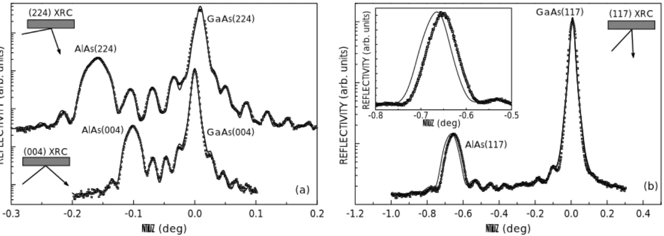
An introduction is given to the most important properties of wurtzite nitride semiconductors: strain and electrical polarization fields of a magnitude not found in other III-V semiconductors. Particular emphasis is paid on [0001] and [1100] oriented layers. In order to correctly account for these phenomena in the samples under investigation, an efficient model for the dynamical simulation of x-ray diffraction (XRD) profiles is formulated and presented for wurtzite and zincblende crystals.
The deposition of GaN buffer layers on two substrates, SiC(0001) andγ-LiAlO2(100), is discussed. The conventional polar [0001] direction is obtained on SiC(0001) substrates. A new degree of freedom for GaN epitaxy is demonstrated by the growth of GaN along a non-polar direction, namely, [1100] onγ- LiAlO2(100). An in-situ strategy for the reproducible growth of these GaN buffers is developed based on reflection high-energy electron diffraction (RHEED). The films are single-phase within the detec- tion limit of high-resolution XRD and exhibit smooth surface morphologies well suited for subsequent growth of heterostructures. The structural properties of these samples are shown to be very sensitive to substrate preparation before growth. Smooth and clean SiC(0001) substrates result in excellent structural properties of GaN(0001) layers whereas GaN(1100) films still suffer from the inferior morphological and chemical quality ofγ-LiAlO2(100) substrates.
Identically designed GaN/(Al,Ga)N multiple quantum wells (MQWs) are deposited on these two types of buffer layers. Significant differences in recombination due to the different orientations of the polar c-axis with respect to the growth direction are detected in photoluminescence (PL). It is demonstrated that flat-band conditions are established in [1100] oriented wells whereas strong electrostatic fields have to be taken into account for the [0001] oriented wells. Consequently, the transition energy of the [0001]
oriented wells is red-shifted with respect to the [1100] oriented wells. Furthermore, [0001] oriented wells exhibit significantly prolonged PL decay times. These results are in quantitative agreement with theoretical predictions based on self-consistent effective-mass Schr ¨odinger-Poisson calculations of the band profiles and wave functions. Finally, while the emission from [0001] oriented wells is isotropic, the emission from [1100] oriented wells is strongly polarized (>90%) normal to the [0001] axis in sound agreement with the different valence band structures of the wells.
The growth of (In,Ga)N/GaN MQWs is studied. Massive In surface segregation (evidenced by RHEED, XRD, secondary-ion mass-spectrometry and PL) is shown to result in top-hat profiles and is therefore a zeroth order process instead of a first order process as observed for other materials systems. In segrega- tion during metal-stable growth results in quantum wells with poor electron-hole wavefunction overlap since the actual well width is much larger than the intended one. Reduction of In segregation by N-stable conditions is possible but inevitably delivers rough interfaces. A strategy for obtaining (In,Ga)N/GaN MQWs with smooth interfaces and high quantum efficiency is devised.
The radiative recombination from (In,Ga)N/GaN MQWs is examined. It is demonstrated that both compositional fluctuations and electrostatic fields have to be taken into account for a thorough under- standing of the emission from these structures. The temperature dependence of the radiative decay time is measured to probe the dimensionality of the system. For a quantitative understanding, a rate- equation model is utilized for analyzing the data. For low temperatures, recombination is governed by localized states whereas for high temperatures extended states dominate. This analysis shows that the localization depth in these structures is below 25 meV.
Zusammenfassung
Thema dieser Arbeit ist die Synthese von hexagonalen (Al,Ga,In)N-Heterostrukturen mittels plasma- unterst ¨utzter Molekularstrahlepitaxie. Die Proben werden entlang der polaren [0001]-Richtung und der unpolaren [1100]-Richtung auf SiC(0001)- bzw.γ-LiAlO2(100)-Substraten gewachsen. Der Einfluß der Wachstumsbedingungen auf die strukturellen, morphologischen, optischen, vibronischen und elektri- schen Eigenschaften der Proben wird untersucht.
Im Vergleich zu den ¨ubrigen III-V-Halbleitern zeichnen sich die hexagonalen Nitride besonders durch die Gr ¨oße ihrer Fehlpassungen und elektrischen Polarisationsfelder aus. Eine Einf ¨uhrung in diese bei- den wichtigen Eigenschaften wird gegeben, insbesondere f ¨ur [0001]- und [1100]-orientierte Schichten.
Um Verspannungen und elektrische Polarisationsfelder in korrekter Art und Weise zu ber ¨ucksichtigen, wird ein effizientes Modell zur dynamischen Simulation von R ¨ontgenbeugungsprofilen formuliert und auf hexagonale sowie kubische Kristalle angewandt.
Die Synthese von GaN-Pufferschichten auf SiC(0001)- undγ-LiAlO2(100)-Substraten wird diskutiert.
Das GaN-Wachstum auf SiC(0001) erfolgt entlang der ¨ublichen polaren [0001]-Richtung. Ein neuarti- ger Freiheitsgrad der GaN-Epitaxie wird durch das Wachstum von GaN entlang der unpolaren [1100]- Richtung aufγ-LiAlO2(100) erreicht. Eine in-situ Strategie zur reproduzierbaren Abscheidung von GaN- Pufferschichten wird erarbeitet, die auf der Kontrolle der Wachstumsparameter durch Beugung von hochenergetischen Elektronen beruht. Die Schichten sind einphasig innerhalb der Nachweisgrenze von R ¨ontgenbeugung und zeichnen sich durch glatte Oberfl¨achen aus, die f ¨ur das weitere Wachstum von Heterostrukturen gut geeignet sind. Es wird gezeigt, daß die strukturellen Eigenschaften der Puffer- schichten sehr stark von der Substratpr¨aparation abh¨angen. Ausgezeichnete strukturelle Eigenschaf- ten werden auf sauberen und glatten SiC(0001)-Substraten erzielt, wogegen GaN(1100)-Filme unter der schlechteren Oberfl¨achenqualit¨at derγ-LiAlO2(100)-Substrate leiden.
GaN/(Al,Ga)N-Multiquantenwells (MQWs) mit identischer Schichtfolge werden auf den beiden Sor- ten von GaN-Pufferschichten gewachsen. Wegen der verschiedenen Orientierungen der polaren c- Achse relativ zur Wachstumsrichtung treten in der Rekombination von Ladungstr¨agern erhebliche Un- terschiede auf. Es wird gezeigt, daß in [1100]-orientieren Wells Flachbandbedingungen herrschen.
Im Gegensatz dazu existieren starke elektrostatische Felder in [0001]-orientierten Wells. Daher ist die Ubergangsenergie von [0001]-orientierten Wells rotverschoben relativ zur ¨¨ Ubergangsenergie der [1100]- orientierten Wells. Weiterhin besitzen die [0001]-orientierten Wells sehr viel l¨angere Zerfallszeiten in der Photolumineszenz (PL). Beide Ergebnisse sind in quantitativer ¨Ubereinstimmung mit theoretischen Vorhersagen, die auf selbstkonsistenten Berechnungen von Bandprofilen und Wellenfunktionen mittels der Poisson- und Schr ¨odingergleichungen in der Effektivmassen-N¨aherung basieren. Die Emission der [0001]-orientierten Wells ist isotrop, w¨ahrend die Emission der [1100]-orientierten Wells stark (>90%) senkrecht zur [0001]-Richtung polarisiert ist. Diese Ergebnisse sind in sehr guter ¨Ubereinstimmung mit den unterschiedlichen Valenzbandstrukturen der Wells.
Das Wachstum von (In,Ga)N/GaN-MQWs wird untersucht. Massive Oberfl¨achensegregation von In wird mit Beugung hochenergetischer Elektronen, Sekund¨arionenmassenspektrometrie, R ¨ontgenbeu- gung und PL nachgewiesen. Rechteckige In-Profile belegen einen Segregationsmechanismus nullter Ordnung und nicht (wie bei anderen Materialsystemen beobachtet) einen erster Ordnung. Diese In- Segregation w¨ahrend des metallstabilen Wachstums resultiert in MQWs mit geringem ¨Uberlapp der Elektronen- und Lochwellenfunktionen, weil die Wells sehr viel dicker als beabsichtigt sind. Eine Ver- minderung der In-Segregation ist m ¨oglich durch N-stabiles Wachstum, f ¨uhrt jedoch zu rauhen Grenz- fl¨achen. Eine Strategie zum Wachstum von MQWs mit glatten Grenzfl¨achen und hohen Quanteneffizi- enzen wird vorgestellt.
Die strahlende Rekombination von (In,Ga)N/GaN-MQWs wird diskutiert. Es wird gezeigt, daß so- wohl Zusammensetzungsfluktuationen als auch elektrostatische Felder f ¨ur ein eingehendes Verst¨andnis der Rekombination ber ¨ucksichtigt werden m ¨ussen. Die Temperaturabh¨angigkeit der strahlenden Le- bensdauer wird gemessen, um die Dimensionalit¨at des Systems aufzukl¨aren. F ¨ur ein quantitatives Verst¨andnis wird ein Ratengleichungsmodell zur Analyse der Daten benutzt. Bei niedrigen Tempera- turen wird die Rekombination von lokalisierten Zust¨ande gepr¨agt, wohingegen ausgedehnte Zust¨ande bei h ¨oheren Tenmperaturen dominieren. Diese Analyse zeigt, daß die Lokalisierungstiefe in diesen Strukturen unterhalb von 25 meV liegt.
Parts of this work have already been published:
P. Waltereit, O. Brandt, A. Trampert, M. Ramsteiner, M. Reiche, M. Qi, and K. H. Ploog, Influence of AlN nucleation layers on growth mode and strain relief of GaN grown on 6H- SiC(0001), Appl. Phys. Lett. 74, 3660 (1999).
P. Waltereit, O. Brandt, and K. H. Ploog, Violet and blue emitting (In,Ga)N/GaN multiple quantum wells grown onγ-LiAlO2(100) by RF plasma-assisted molecular beam epitaxy, Appl.
Phys. Lett. 75, 2029 (1999).
O. Brandt, R. Muralidharan, P. Waltereit, A. Thamm, A. Trampert, H. von Kiedrowski, and K. H. Ploog, Critical issues for the growth of high quality (Al,Ga)N/GaN and GaN/(In,Ga)N heterostructures on SiC(0001) by molecular beam epitaxy, Appl. Phys. Lett.
75, 4019 (1999).
O. Brandt, R. Muralidharan, A. Thamm, P. Waltereit, and K. H. Ploog, Essential strate- gies for the growth of high-quality (Al,Ga)N/GaN and GaN/(In,Ga)N heterostructures on SiC(0001) by molecular beam epitaxy, Proceedings 10th International Workshop on the Physics of Semiconductor Devices, Delhi (India) 1999, edited by V. Kumar and S. K.
Agarwal (Allied Publishers Ltd., New Delhi, 2000), 1495–1506.
P. Waltereit, O. Brandt, M. Ramsteiner, and K. H. Ploog, Growth of M-plane GaN/(Ga,In)N heterostructures: way out of the dilemma of electrical polarization in nitrides, Proceedings 3rd SANKEN International Symposium on Advanced Nanoelectronics:
Devices, Materials and Computing, Osaka (Japan) 2000, Memoirs of the ISIR Vol. 57, 171 2000.
O. Brandt, R. Muralidharan, A. Thamm, P. Waltereit, and K. H. Ploog, Key issues for the growth of high-quality (Al,Ga)N/GaN and GaN/(In,Ga)N heterostructures by molecular beam epitaxy, Proceedings 10th International Conference on Solid Films and Surfaces, Princeton (USA) 2000. Appl. Surf. Sci. 175, 419 (2001).
P. Waltereit, O. Brandt, A. Trampert, H. T. Grahn, J. Menniger, M. Ramsteiner, M. Re- iche, and K. H. Ploog, Nitride semiconductors free of electrostatic fields for efficient white light-emitting diodes, Nature 406, 865 (2000).
P. Waltereit, O. Brandt, M. Ramsteiner, K. H. Ploog, R. Uecker, and P. Reiche, Growth of M-plane GaN(1 ¯100)onγ-LiAlO2(100), J. Cryst. Growth 218, 143 (2000).
P. Waltereit, O. Brandt, M. Ramsteiner, J. Ringling, A. Trampert, and K. H. Ploog, Coex- istence of electric fields and composition fluctuations in (In,Ga)N/GaN quantum wells grown on 6H-SiC(0001), 26th Internat. Symposium on Compound Semiconductors, Berlin (Germany) 1999, Int. Phys. Conf. Ser. No. 166, 453 (2000).
P. Waltereit, O. Brandt, M. Ramsteiner, and K. H. Ploog, M-plane GaN(1¯100): a way to evade polarization fields in nitrides, Proc. 3rd International Symposium on Blue Laser and Light Emitting Diodes (ISBLLED), Zeuthen (Germany) 2000, phys. stat. sol. (a) 180, 133 (2000).
K. H. Ploog, O. Brandt, R. Muralidharan, A. Thamm, and P. Waltereit, Growth of high quality (Al,Ga,In)N heterostructures on SiC(0001) by both plasma-assisted and reactive MBE, 27th Conference on the Physics and Chemistry of Semiconductor Interfaces, Salt Lake City (USA) 2000, J. Vac. Sci. Technol. B 18, 2290 (2000).
B. Rau, P. Waltereit, O. Brandt, M. Ramsteiner, K. H. Ploog, J. Puls and F. Henneberger, In-plane polarization anisotropy of the spontaneous emission of M-plane GaN/(Al,Ga)N quan- tum wells, Appl. Phys. Lett. 77, 3343 (2000).
P. Waltereit, O. Brandt, M. Ramsteiner, A. Trampert, H. T. Grahn, J. Menniger, M. Re- iche, and K. H. Ploog, M-plane GaN(1¯100) grown onγ-LiAlO2(100): nitride semiconduc- tors free of internal electric fields, 11th International Conference on Molecular Beam Epi- taxy, Beijing (China) 2000, J. Cryst. Growth 227, 437 (2001).
M. Giehler, M. Ramsteiner, P. Waltereit, O. Brandt, and K. H. Ploog, Substrate dependent halfwidth and frequency of the E2(high) phonon line in GaN studied by Raman spectroscopy, J.
Appl. Phys. 89, 3634 (2001).
O. Brandt, P. Waltereit, and K. H. Ploog, Determination of strain-state and composition of highly mismatched group-III nitride heterostructures by x-ray diffraction, Phys. Rev. B (sub- mitted).
H. T. Grahn, A. Thamm, P. Waltereit, O. Brandt, and K. H. Ploog, Influence of internal electric fields on the carrier dynamics in GaN/(Al,Ga)N multiple quantum wells with different orientation and strain state, International Workshop on Nitride Semiconductors, Nagoya (Japan) 2000, Jpn. J. Appl. Phys. (to be published).
B. Rau, J. Puls, F. Henneberger, P. Waltereit, O. Brandt, M. Ramsteiner, and K. H.
Ploog, Comparative study of the spontaneous and stimulated emission of M- and C-plane GaN/(Al,Ga)N quantum wells, Proceedings of SPIE Vol. 4283 (to be published).
C. Cobet, N. Esser, J. T. Zettler, W. Richter, P. Waltereit, O. Brandt, K. H. Ploog, S. Peters, N. V. Edwards, O. P. A. Lindquist, and M. Cardona, Optical properties of wurtzite AlGaN parallel and perpendicular to the optical axis, Phys. Rev. B (to be published).
P. Waltereit, O. Brandt, K. H. Ploog, M. A. Tagliente, and L. Tapfer, In-surface segregation during growth of (In,Ga)N/GaN multiple quantum wells by plasma-assisted molecular-beam epitaxy, Phys. Rev. B (submitted).
P. Waltereit, O. Brandt, J. Ringling, and K. H. Ploog, Electrostatic fields and compositional fluctuations in (In,Ga)N/GaN multiple quantum wells grown by plasma-assisted molecular beam epitaxy, Phys. Rev. B (submitted).
S. Ghosh, P. Waltereit, O. Brandt, H. T. Grahn, and K. H. Ploog, Polarization-dependent spectroscopic study of M-plane GaN onγ-LiAlO2, Appl. Phys. Lett. (submitted).
P. Waltereit, O. Brandt, K. H. Ploog, M. A. Tagliente, and L. Tapfer, In-surface segregation during growth of (In,Ga)N/GaN multiple quantum wells by plasma-assisted molecular-beam epitaxy, Proc. 4th International Conference on Nitride Semiconductors (ICNS), Denver (USA) 2001, phys. stat. sol. (to be published).
Patent application:
P. Waltereit, O. Brandt, and K. Ploog, Highly efficient UV emitter on the basis of hexagonal nitrides, European Patent Application Nr. PCT/EP00/11044.
Contents
1 Introduction 6
2 Strain and electrical polarization fields in wurtzite nitride semiconductors 10
2.1 Strain and stress . . . 10
2.2 Optical and vibrational deformation potentials . . . 12
2.3 Electrical polarization . . . 14
2.4 Internal electrostatic fields due to electrical polarization . . . 16
3 Dynamical x-ray diffraction for accurate determination of strain state and composition of highly-mismatched group-III nitrides 19 3.1 Accurate kinematical analysis of x-ray diffraction profiles . . . 19
3.2 From the kinematical to the dynamical analysis . . . 21
3.3 Scans in reciprocal and real space . . . 22
3.4 Formulation of the model . . . 24
3.5 Application to arsenide and nitride samples . . . 27
4 Development and optimization of GaN heteroepitaxy on SiC(0001) and γ-LiAlO2(100) 32 4.1 MBE system and substrate mounting . . . 32
4.2 Choice of SiC(0001) andγ-LiAlO2(100) substrates . . . 33
4.3 Crystal structures of the substrate surfaces and orientational relationships 36 4.4 Substrate preparation before growth . . . 37
4.5 Impact of AlN and GaN nucleation layers on SiC(0001) . . . 40
4.6 Optimization of nucleation . . . 44
4.7 Detection and adjustment of surface stoichiometry during growth . . . . 46
4.8 Optimization of growth temperature . . . 48
5 Characterization of GaN(0001) and GaN(1100) 51 5.1 Atomic force microscopy . . . 51
5.2 X-ray diffraction . . . 52
5.3 Raman scattering . . . 55
5.4 Ellipsometry and Photoluminescence . . . 56
5.5 Capacitance-voltage profiling and Hall measurements . . . 60
6 GaN/(Al,Ga)N multiple quantum wells and the role of crystal orientation on emission 62 6.1 Growth and structural investigation of GaN/(Al,Ga)N heterostructures 62 6.2 Role of crystal orientation on emission from GaN/(Al,Ga)N MQWs . . . 66
7 Synthesis of (In,Ga)N/GaN multiple quantum wells 72
7.1 Critical issues for (In,Ga)N growth . . . 72
7.2 RHEED observations . . . 73
7.3 Detection of In segregation by SIMS and XRD . . . 74
7.4 Impact of In segregation on photoluminescence . . . 78
8 Electrostatic fields and compositional fluctuations in (In,Ga)N/GaN multiple quantum wells 81 8.1 Different emission mechanisms . . . 81
8.2 Electrostatic fields . . . 82
8.3 Energy and temperature dependence of the radiative decay time . . . 84
9 Conclusion and Outlook 88
A Origin of-high energy shoulders of (In,Ga)N/GaN MQW PL spectra 90
Bibliography 93
Danksagung 100
Lebenslauf 102
Selbstst¨andigkeitserkl¨arung 103
1 Introduction
GeneralThe 20th century has been coined the age of solid-state-electronics, as the re- placement of vacuum tubes with transistors had revolutionary impact on the economic and sociological aspects of our society. At the advent of the 21st century, an analogous technological transition takes place which is culminating in the age of solid-state pho- tonics. Modern communication technology has been made possible by optoelectronic devices, such as light-emitting diodes (LEDs) and laser diodes (LDs). Furthermore, Edison’s fragile and bulky light bulb is beginning to be replaced by rugged and com- pact solid state lamps based on light-emitting diodes (LEDs). In fact, initiators of these two revolutions (Z. Alferov, J. Kilby and H. Kroemer) have been awarded with the physics Nobel prize 2000.
The first LEDs were demonstrated by General Electric in 1962 and commercialized in 1968 by Monsanto and Hewlett-Packard. However, throughout the 1970’s and 1980’s, the electrical-to-optical power efficiency of these devices was well below that of conventional incandescent lamps (12 lm/W). Moreover, only group-III arsenides and phosphides were utilized as LED materials thus restricting the available colors from red to green. Therefore, the use of these low brightness LEDs was limited to indoor indicator applications. During the last decade, however, the technology of LEDs has improved remarkably in two ways. First, higher conversion efficiencies (more than 100 lm/W for red LEDs) are obtained. Second, the entire visible spectrum is now cov- ered including green (30 lm/W) and blue (10 lm/W).
These high brightness LEDs have reached the status of illuminators, hence, mak- ing them (in the case of red LEDs) superior to the most efficient conventional light sources such as halogen and fluorescent lamps (70 lm/W). The replacement of conven- tional light sources by LEDs will have vast economic and ecological consequences. At present, the total value of LEDs shipped worldwide amounts to $2 billion, one quarter being high brightness LEDs. [1] The replacement of all traffic lights by LEDs would save around 2.5 billion kWh annually in the USA. [2] White LEDs, as used for lighting applications, are realized either by combining red, green and blue LEDs or by employ- ing a blue/ultraviolet (UV) LED which excites a phosphor to achieve the white color impression. Short-wavelength LDs pave the way to additional important applications, namely data storage and color printing/copying. Data storage densities and printer resolutions scale inversely with the square of the LD wavelength. Many other potential applications for short wavelength devices can be envisaged, such as, e.g., solar-blind photo-detectors, x-ray detectors or accousto-optical modulators.
Prime candidates for all of these short wavelength applications are the group-III ni- trides (Al,Ga,In)N whose band gap can be continuously tuned from the ultraviolet (6.1 eV for AlN) to the red (1.8 eV for InN). Moreover, their excellent thermal, mechan- ical and chemical stabilities make them ideal even for applications in hostile environ- ments.
In the following, a brief history of the group-III nitrides is given. GaN was synthesized for the first time by Johnson et al. [3] in 1932 by passing ammonia over hot Ga. This method produced small GaN needles and platelets. The other nitride semiconductors, AlN and InN, were fabricated in 1928 by Tiede et al. [4] and in 1938 by Juza et al. [5], respectively. The first epitaxial growth of GaN was achieved in 1969 by Maruska and
Tietjen [6] by a chloride vapor transport technique to obtain large-area layers of GaN on sapphire. Pankove et al. [7] realized the first electroluminescence from GaN. They employed an Zn doped n-type GaN metal-insulator-semiconductor diode that could emit either blue, green, yellow or red light depending on the Zn doping level. How- ever, the efficiency of these devices was very low. The fabrication of actual pn-junctions was impeded by the fact that GaN was always highly n-type, even when not deliber- ately doped. The first p-type doped GaN was reported by Akasaki et al. [8] in 1988 and Amano et al. [9] in 1989 after electron beam treatment of Mg doped GaN. Further devel- opment of the nitrides is unthinkable without Shuji Nakamura from Nichia Chemicals (Japan) leading to the commercialization of ultraviolet, blue and green high-brightness LEDs [10] in 1993 and finally blue/ultraviolet continuous-wave injection LDs [10] in 1996. It should be noted here that the lifetime of these laser (more than 10,000 h) well exceeds that (below 400 h) of blue-green lasers based on II-VI compounds.
Group-III nitrides are usually grown by two different techniques, either metal-organic chemical vapor deposition (MOCVD) or molecular beam epitaxy (MBE). For a long time, MOCVD delivered crystals having a better overall quality. The inferior quality of MBE grown material mainly originated from technological issues. In particular, nitrogen sources for MBE were very inefficient and of rather low purity. At the time of starting this PhD project (March 1998), group-III nitrides grown by MBE exhibited very rough interfaces and surfaces, high dislocation densities as well as poor optical and electrical data.
However, in the last two years, MBE has become a competitive technique for elec- tronic device applications of nitrides. In fact, the best mobilities of GaN/(Al,Ga)N two-dimensional electron gases were reported for MBE grown samples. [11] In con- trast, the field of nitride optoelectronics is still controlled by MOCVD.
Despite the successful realization of high brightness LEDs and injection LDs, there is still a lack of knowledge about many fundamental properties of nitrides. Generally, the impact of growth conditions of (Al,Ga,In)N on the materials properties is still under debate. (In,Ga)N/GaN multiple quantum wells (MQWs) are used in LEDs and LDs, but only little insight into the actual structural properties of these MQWs, in particular their interfaces, has been gained yet. Moreover, the optical properties of these struc- tures are still controversially discussed in terms of compositional fluctuations and/or strong electrostatic fields.
The foundation for the tailored growth and the understanding of properties of thin layers is the study of their fundamental growth processes. Investigations of the im- pact of growth temperature and surface stoichiometry on epilayer deposition are the strength of MBE due to its in-situ tools, such as reflection high energy electron diffrac- tion (RHEED). This technique has become extremely valuable for the understanding of growth mechanisms of thin films.
MBE of nitrides can be divided into two approaches, reactive MBE (RMBE) and plasma-assisted MBE (PAMBE), depending on the nitrogen precursor. In RMBE, am- monia is catalytically cracked on the sample surface to deliver active nitrogen, whereas in PAMBE the chemically inert nitrogen molecule is activated by a plasma discharge.
Hence, the amount of active nitrogen is coupled to the deposition temperature in RMBE analogously to the case of MOCVD. In contrast, the amount of active nitrogen is independent of deposition temperature in the case of PAMBE, thus allowing rather
flexible growth parameters. PAMBE enables low-temperature growth while maintain- ing an arbitrarily high nitrogen flux as required, e.g., for (In,Ga)N/GaN MQWs.
Aim of this work The above mentioned variety of issues already outlines the objec- tives of the present work. The overall objective is to investigate the individual steps required for the growth of a blue/UV LED by PAMBE. These steps range from the choice of a suitable substrate, over the synthesis of GaN layers to the deposition of (In,Ga)N/GaN and GaN/(Al,Ga)N MQWs. The quality of the samples is desired to be high and reproducibly so. In addition to these goals related to crystal growth, it is aimed to gain insight into the structure-property relationship of (Al,Ga,In)N.
This thesis is organized as follows. Starting point in Chapter 2 is the understanding of the most important properties of wurtzite nitrides semiconductors: strains and elec- trical polarization fields of a magnitude not found in other III-V semiconductors. In order to correctly account for these phenomena, an accurate structural characteriza- tion (e.g. composition, strain state and structural integrity) of all samples is manda- tory. Therefore, in Chapter 3, an efficient model for the dynamical simulation of x-ray diffraction (XRD) profiles is developed. In Chapter 4, the deposition of GaN buffer layers on two substrates, SiC(0001) andγ-LiAlO2(100), is discussed. Compared to the ubiquitous sapphire substrate, these alternative substrates offer—in principle—a vari- ety of promising advantages such as a smaller lattice mismatch to GaN(0001), a high thermal and electrical conductivity [(SiC(0001)] and selectivity in wet-chemical etching [γ-LiAlO2(100)]. At the beginning of this work, both substrates were very rarely used and their preparation and handling was still in its infancy. Development and optimiza- tion of substrate preparation is necessary for the reproducible growth of high quality structures.
The most interesting discovery in Chapter 4 is the formation of the non-polar M-plane GaN(1100) onγ-LiAlO2(100) substrates in contrast to the polar C-plane GaN(0001) ori- entation obtained on SiC(0001) and Al2O3(0001). Based on this finding, the following investigations were motivated. In Chapter 5, a direct comparison of the properties of C-plane and M-plane GaN epilayers grown under optimized conditions is presented.
The results demonstrate the impact of crystal orientation of the GaN films on their morphological, structural, optical and vibrational properties. The by far most inter- esting difference between these two orientations manifests itself in thin films such as MQWs. The conventional C-plane oriented MQWs exhibit strong electrostatic fields since the polar c-axis of GaN is parallel to the growth direction. These fields lead to a quantum-confined Stark-effect and a substantial reduction in room temperature quan- tum efficiency. In contrast, M-plane oriented MQWs are free of these fields because the c-axis of GaN is normal to the growth direction. Furthermore, an in-plane anisotropy of the spontaneous emission from M-plane oriented MQWs is found. Chapter 6 cov- ers growth, structural and optical characterization of GaN/(Al,Ga)N MQWs which are ideally suited model systems for studying recombination properties of group-III nitride MQWs due to their high structural perfection. The photoluminescence (PL) results are in excellent agreement with the theoretical predictions.
Chapter 7 treats the synthesis of (In,Ga)N/GaN MQWs which are required for LEDs emitting in the visible spectral range. Growth of (In,Ga)N/GaN MQWs is impeded by In surface segregation as well as spinodal and thermal decomposition. Compared to MOCVD and RMBE, very low growth temperatures can be used in PAMBE to explore
deposition of these MQWs far away from thermodynamic equilibrium. Understand- ing the In surface segregation turns out to be crucial for the realization of high quality (In,Ga)N/GaN MQWs. This segregation manifests itself in RHEED, XRD, secondary- ion-mass-spectrometry (SIMS) and photoluminescence (PL). Finally, the radiative re- combination from (In,Ga)N/GaN MQW is studied in Chapter 8. It is shown that both compositional fluctuations and electrostatic fields have to be taken into account for a thorough understanding of the emission from these structures.
A large variety of characterization techniques is employed in this thesis. Experimental details are not presented in a separate Chapter but are given at the relevant part of the text.
2 Strain and electrical polarization fields in wurtzite ni- tride semiconductors
This Chapter gives an introduction to two of the most important properties of wurtzite nitride semiconductors: strains and polarization fields of a magnitude not found in other III-V semiconductors. First, the consequences of strains on the structural, optical and vibrational properties are presented. Then, the impact of the huge spontaneous and piezoelectric polarization fields on radiative recombination from quantum wells is outlined. Each subject is discussed for an arbitrary crystal orientation as well as for the special cases of C-plane [0001] and M-plane [1100] oriented quantum wells.
2.1 Strain and stress
Group-III nitrides constitute a materials systems with individual lattice mismatches of several percent. A proper treatment of strains and stresses is therefore required in order to correctly describe all phenomena involving strain, e.g., piezoelectric polarization. In this section, the concept of strain and stress is outlined and applied to the two growth directions employed in this thesis, namely, [0001] and [1100].
Unit cell geometryThe equilibrium structure of the group-III nitrides is wurtzite. The hexagonal unit cell (Fig. 2.1) is defined by the edge length a of the basal hexagon, the height c of the hexagonal prism, and an internal parameter u defined as the anion- cation bond length along the [0001] axis in units of c. Here, we will restrict ourselves to the elastic properties of this unit cell type. The primitive translational vectors a1, a2 and a3are readily expressed in terms of the unstrained lattice constants ar and cr by
a1 =arˆex, a2 = ar 2 ˆex+
p
3 ar
2 ˆey, a3 =crˆez (2.1) with the set of orthonormal basis vectors (ˆex, ˆey, ˆez) in a Cartesian frame of reference.
The vector a3is parallel to the c-axis and normal to the basal plane which is defined by a1and a2. The angle between the two latter vectors is 120Æ.
ex ez
cr
ar a1
a2
a3
ey
C-plane M-plane
Figure 2.1: Geometry of the unstrained unit cell of nitride semiconductors with the primitive translation vectors ai and the set (ˆex, ˆey, ˆex) of Cartesian unit vectors. ar and cr denote the unstrained lattice constants. The light and dark shaded areas correspond to the M-plane and the C-plane, respectively.
Strain tensorThe strain tensor is used to describe changes of the unit cell geometry due to distortion. In the case of strain, the lengths and/or the directions of the primitive translational vectors are modified. These modified vectors are then expressed using Eq. (2.1) by a new set of basis vectors e0x, e0y and e0z in a linear superposition of ˆex, ˆey and ˆez. For a general strain, we obtain
e0x = (1+xx)ˆex + xy ˆey + xz ˆez e0y = yx ˆex + (1+yy)ˆey + yz ˆez e0z = zx ˆex + zyˆey + (1+zz)ˆez
(2.2) with the strain tensor elementsi j. The strain tensor may be separated in a symmet- ric and an asymmetric part. The former contains normal and shear strains while the latter expresses any rotation of the unit cell. [12] For a given sample, one can mea- sure all components of the distortion tensor by a thorough analyis of x-ray diffraction scans. [13] For the samples under investigation in this work, it has been shown by x-ray diffraction that rotations of the unit cells are, if any, negligible. The distortion tensor is thus symmetric and from hereon called strain tensor. This tensor consists of normal strain componentsxx,yy andzz as well as shear strain componentsxy,xz andyz. Stress tensorThe stress tensor expresses the pressure which is applied to the crystal. In the present case, the stress tensor is symmetric since the strain tensor is also symmetric.
There are normal stressesσxx, σyy and σzz as well as shear stressesσxy, σxz andσyz. The stress and strain tensors are related via the elastic properties of the crystal in the generalization of Hooke’s law for systems having more than one degree of freedom.
In general, this generalization readsσi j = Ci jklkl (Einstein sum convention) with the elements Ci jkl of the stress-strain tensor. However, in our case both the stress and the strain tensor are symmetric such that we can simplify this relation. Both the stress and the strain tensors are written as (pseudo-)vectors with 6 elements (Voigt scheme [14]). Consequently, the stress-strain tensor Ci j is of (pseudo-)second-rank instead of the original fourth-rank form Ci jkl. Furthermore, we take into account the symmetry of the hexagonal unit cell for the symmetry of the stress-strain tensor and arrive at [14]
0
B
B
B
B
B
B
@
σxx
σyy
σzz
σyz
σxz
σxy
1
C
C
C
C
C
C
A
= 0
B
B
B
B
B
B
@
C11 C12 C13 0 0 0 C12 C11 C13 0 0 0 C13 C13 C33 0 0 0
0 0 0 C44 0 0
0 0 0 0 C44 0
0 0 0 0 0 C66
1
C
C
C
C
C
C
A 0
B
B
B
B
B
B
@
xx
yy
zz
yz
xz
xy
1
C
C
C
C
C
C
A
(2.3)
In the following, we will apply this expression to epitaxial layers grown along the [0001] or [1100] direction. In both orientations, shear stresses and shear strains are absent since the angles between the primitive translational vectors [Eq. (2.1)] are con- served by stress along one of the unit vectors ˆex, ˆeyor ˆez. A useful boundary condition is the fact that epitaxial films do not experience stress along the growth direction as they are free to expand or contract along this direction. This fact allows us to derive expressions for the strain along the growth direction as a function of the strains within the growth plane.
Strain for growth along [0001]In this orientation, the growth plane corresponds to the xy-plane and deposition takes place along the z direction. The treatment of this ori-
entation is simplified by the fact that the in-plane strain is always isotropic for growth on SiC(0001) as performed in this thesis. Consider an epitaxial layer with unstrained lattice constants ar and cr which is grown on a [0001] oriented, lattice mismatched sub- strate with lattice constants as and cs. Depending on the relaxation of the in-plane lattice mismatch (ar as)=as, the deposited epilayer has the lattice constants a and c. Hence, the films is under biaxial strain characterized by an isotropic in-plane com- ponentk = (a ar)=ar = xx = yy within the growth plane and an out-of-plane component? =(c cr)=cr =zz along the growth direction (an analogous notation is used for the stress tensor elements).
Eq. (2.3) now reads
σk σ?
=
C11+C12 C13 2C13 C33
εk ε?
(2.4) Since the film is free of stress along the growth direction (σ? =0) we obtain
?
k = 2 C13
C33 (2.5)
which describes Poisson’s effect. An epilayer under compressive in-plane strain will expand along the growth direction and vice versa. The in-plane stressσkand in-plane strainkare related by the Young modulus
Y=C11+C12 2C213=C33 (2.6) viaσk =Yk. Note that this equation is equivalent to Hooke’s law within the growth plane.
Strain for growth along [1100] In this orientation, the growth plane corresponds to the xz-plane, growth takes place along the y direction. The in-plane strain of a lattice mismatched grown epilayer is, in general, not isotropic (xx 6= zz) in contrast to the [0001] growth direction. Nevertheless, one can readily derive a relation for the out-of- plane strain as a function of the two in-plane strains in analogy to the [0001] growth direction. We obtain
yy = C12xx C13zz
C11 (2.7)
which is the analogue of Eq. (2.5) of the [0001] orientation.
Choice of materials constants The use of the concept of strain and stress critically relies on the choice of materials parameters. Consequently, great care is used in this work to use the most recent and most reliable data for the unstrained lattice constants and elastic constants (Tab. 3.1). To be as consistent as possible in this thesis, also the optical and vibrational deformation potentials in the next section are taken from the same reference as the elastic constants. [15]
2.2 Optical and vibrational deformation potentials
In this section, we will discuss the consequences of strain on the band gap energy and phonon energies of epitaxial layers. In the course of this thesis, these relations are often used, e.g., in order to support strains determined by x-ray diffraction.
Hydrostatic and uniaxial strainFor both the optical and the vibrational properties, it is generally useful to express the strain state of the unit cell in terms of a hydrostatic strain hand an uniaxial strainualong the c-axis which conserves the unit cell volume. The latter requirement is—to first order—fulfilled if the sum of the normal strains is zero.
Hence, we re-write the strain state in terms ofhanduas
0
@
xx
yy
zz
1
A
=h
0
@
1 1 1
1
A
+u
0
@
1 α
(1+α)
1
A (2.8)
with the parameter α. This equation can be solved using the boundary conditions given by Eq. (2.5) and (2.7). For the C-plane orientation we get
h =
1 3
2k+?
, u = 1 3
k+?
(2.9) while the corresponding expressions for M-plane are
h =
(C11 C12)xx+(C11 C13)zz
3C11 , u =
(C11+2C12)xx+(C13 C11)zz
3C11
(2.10) Optical propertiesA compression of the unit cell will, at least in case of all III-V semi- conductors, result in a blue-shift of intrinsic optical transitions whereas an expansion leads to a red-shift in emission and absorption. In the quasicubic approximation, [15]
the transition energy associated with the free A exciton ( 1c 6v) of wurtzite nitrides is shifted according to
EA =3agh
3 2
d5
p
6u (2.11)
with the deformation potentials ag and d5. This expression is valid for small strains and is then exact for [0001] oriented samples but only an approximation in the case of [1100] oriented films. The numerical values of the deformation potentials used in this thesis are listed in Tab. 2.1.
Vibrational properties The E2 phonon mode is generally used to examine the strain state of GaN by Raman measurements. A linear superposition of hydrostatic and uni- axial components is also assumed to be valid for the frequency shift ωE2 of the E2 phonon. Hence, we find
ωE2 =3ωγh+βu (2.12)
Table 2.1: Optical deformation potentials (eV) in the quasi-cubic approximation for wurtzite nitride semiconductors. [15]
Material ag d5 GaN -6.9 -5.3
AlN -9.0 -7.5 InN -2.8 - 3.8
where ω is the E2 phonon wave number and β a constant. γ=∂lnω=∂ln V is the Gr ¨uneisen parameter which relates relative changes in phonon frequencies to relative changes of the unit cell volume.
Once again, the value of ωE2 substantially depends on the correct choice of mate- rials constants. We use the same ab-initio calculations [15] as before to extract the Gr ¨uneisen parameter of γ=1.8 for GaN. The E2 mode of unstrained GaN has a fre- quency of ω=566.2 cm 1 [16]. The constantβ=5692 cm 1 is deduced by comparison Eq. (2.12) to recent experimental results. [16]
2.3 Electrical polarization
A sizable red-shift of the ground-level transitions of wurtzite nitride semiconduc- tor quantum wells has been observed by various groups [17–20] for increasing well width. This phenomenon is sometimes accompanied by the concomitant reduction of the oscillator strength and by the increase of the decay time of the transition. All to- gether, these effects point towards the existence of strong built-in electrostatic fields in wurtzite nitride semiconductors, which causes a substantial quantum-confined Stark effect (QCSE). The underlying phenomenon is the presence of huge electrical polariza- tion fields in wurtzite nitride semiconductors: The spontaneous polarizations are of the same order of magnitude as those of ferroelectrics. The magnitude of the piezo- electric constants exceeds that of other III-V semiconductors by more than one order of magnitude.
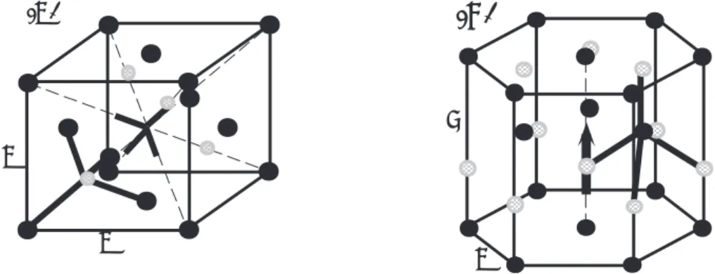
GaN unit cell symmetries The presence of electrical polarization is strongly con- nected to the unit cell symmetry of a crystal. Nitride semiconductors exist in both the zincblende and wurtzite modifications which are closely related to each other.
Ball-and-stick models of these two structures are given in Fig. 2.2. In both cases, each group-III atom is tetrahedrally coordinated to four nitrogen atoms. The main differ- ence between these two structures is the stacking sequence of close packed diatomic planes. These stacking sequences are ABABAB along the wurtzite f0001g directions and ABCABC along the zincblende f111g directions. This difference in stacking se- quence results in distinct space group symmetries: P63mc for wurtzite and F43m for zincblende.
In the absence of external electric fields, the total macroscopic polarization P of a solid is the sum of the spontaneous polarization of the equilibrium structure and of the strain-induced, piezoelectric polarization.
Spontaneousy polarization The zincblende compound semiconductors such as, e.g., GaAs or GaN have four symmetry equivalent polar h111i axes whose contributions cancel each other in equilibrium. Hence, these materials are free of electrical polariza- tion at equilibrium. In contrast, the wurtzite phase has a singular polar axis, namely, the [0001] axis. Thus, the wurtzite phase carries spontaneous electrical polarization along [0001] even at equilibrium.
Piezoelectric polarization In practice, semiconductor layers are often grown under
There also exists the high-pressure rocksalt modification.
ySometimes the term ’pyroelectric polarization’ is used as the magnitude of the spontaneous polar- ization changes with temperature due to thermal expansion of the crystal.
(a) (b)
a a
c a
Figure 2.2: Ball-and-stick models of crystals with zincblende (a) and wurtzite (b) structure. Note the tetrahedral coordination in both cases.
strain due to the lattice mismatch to the underlying layer. Such deformations of the unit cell can lead to additional piezoelectric polarization. The presence of this kind of polarization is again closely related to the unit cell symmetry, namely, the lack of inversion symmetry. The contributions of the four polar axes of zincblende structures cancel each other for growth along a h001i direction. However, growth along one of the polar axes lifts the symmetry and the crystal exhibits piezoelectric polarization. In contrast, the wurtzite structure with its unique polar [0001] axis always carry piezo- electric polarization for any growth direction.
In the following, we discuss nitride semiconductors in this wurtzite structure. The total electric polarization P is the sum of spontaneous polarization PSP and piezoelectric polarization PPZ.
In general, the unit cell can be under arbitrary strain. The piezoelectric polarization is calculated using the piezoelectric tensor [21] of the space group P63mc by
PPZ =
0
@
0 0 0 0 e15 0
0 0 0 e15 0 0
e31 e31 e33 0 0 0
1
A 0
B
B
B
B
B
B
@
xx
yy
zz
yz
xz
xy
1
C
C
C
C
C
C
A
= 0
@
e15xz
e15yz
e31(xx+yy)+e33zz
1
A
(2.13) with the elements ei jof the piezoelectric tensor, the uniaxial strain componentsxx,yy, zz and the shear strainsxy,xz,yz.
For growth along [0001], it is expected that shear strain is absent. As already mentioned in section 2.1, this assumption has been verified by x-ray diffraction for the samples under investigation. Additionally, the in-plane strain is isotropic (xx =yy). With the usual conventionsk =xxand? =zz we arrive at
PPZ,[0001] =e33?+2e31k (2.14) with the piezoelectric constants e33 and e31 and the elastic constants C13 and C33. Hence, the piezoelectric polarization is along [0001].
For growth along [1100], we can also simplify Eq. (2.13). Again, no shear strain is present in the growth plane, hence, both xz and yz vanish. The total piezoelectric
Table 2.2: Spontaneous polarization and piezoelectric constants (both in units of C m 2) of wurtzite group-III nitride semiconductors. [25]
PSP e33 e31 AlN 0.081 1.46 0.60 GaN 0.029 0.73 0.49 InN 0.032 0.97 0.57 polarization is parallel to [0001] and has the magnitude
PPZ,
[1100] =e31(xx+yy)+e33zz (2.15) Polarization constants Materials constants of group-III nitrides are generally deter- mined in ab-initio density-functional theory (DFT) calculations in the framework of the local-density approximation (LDA). The data obtained have been shown to be in ex- cellent agreement with experimental values (see, e.g., [15]). In the case of spontaneous and piezoelectric polarization constants, it is important to note that these materials constants critically rely on structural data such as, e.g., the lattice constant ratio c=a and the anion-cation bond length uc along the [0001] axis. Ideally, the wurtzite struc- ture has c=a=5/3 and u=3/8 but the actual values [22, 23] found for GaN, AlN and InN significantly deviate from these ideal values. Very recently, is it was demonstrated by Bechstedt et al. [24] that even small uncertainties in the structural parameters sub- stantially modify the calculated polarization constants. This statement is particularly important for InN as the lattice constants of this material are subject to a large uncer- tainty due to lack of reliable experimental data.
In this thesis, the polarization constants determined by Bernadini et al. [25] are used (Tab. 2.2). These parameters are obtained by DFT-LDA using the Berry phase ap- proach to the polarization of solids. For several years, these data constituted the only available values apart from the very recent work of Bechstedt et al. [24] who obtained significantly different absolute parameters in their approach. However, the strength of electrostatic fields in thin layers only depends on the differences in electrical po- larization between well and barrier material as shown below. In fact, for the struc- turally well-known GaN/(Al,Ga)N system the two sets of data result in electrostatic fields of very comparable magnitude. In contrast, the predicted electrostatic fields in the (In,Ga)N/GaN system scatter, most probably due to the lack of reliable structural data. From the data of Bernadini et al. [25] (Tab. 2.2) one can calculate the total polar- ization P of (Al,Ga,In)N layers. After having clarified the origin (unit cell symmetry), the direction (parallel to [0001] for C-plane and M-plane MQWs) and the magnitude of electrical polarization [Eq. (2.14), (2.15)] we now turn to the consequences of these fields. In the following, we will show that polarization changes normal to interfaces induce internal electrostatic fields which can be as strong as several MV/cm.
2.4 Internal electrostatic fields due to electrical polarization
In this section, the consequences of electrical polarization on [0001] and [1100] oriented quantum wells are discussed. It will be shown that the former exhibit strong internal
AlN AlN AlN AlN GaN GaN GaN (a)GaN
P
+- - - + + +
- AlN
AlN AlN AlN GaN GaN GaN GaN
E
(b) 0 5 10 15 20 25
-4 -2 0 2 4
2.79 eV (c)
h e
EV EC
ENERGY (eV)
DEPTH (nm)
Figure 2.3: Effect of electrical polarization on a (3 nm GaN)/(3 nm AlN) MQW with 3 periods grown coherently on a GaN(0001) buffer. The changes in total polarization of the individual layers lead to interface charges (a) which result in strong internal electrostatic fields (b). Note the red-shift of the transition energy with respect to flat-bands conditions (Quantum-confined Stark-effect) and the spatial separation of electron (e) and hole (h) wavefunction (c).
electrostatic fields normal to the wells whereas the latter are free of these fields.
[0001] oriented quantum wells: Electrostatic fieldsIn this orientation the growth di- rection is parallel to the total polarization vector. Any discontinuity P in the polar- ization component results in a sheet charge densityP at the corresponding interface or surface. [26] For example, consider a GaN/AlN superlattice with thicknesses tGaN and tAlN grown coherently on a GaN(0001) buffer layer (Fig. 2.3). The total polar- ization of unstrained GaN and coherently strained AlN differs, resulting in charges with alternating sign which are built up at the interfaces and the surface [Fig. 2.3(a)].
These interface charges result in internal electrostatic fields EGaN and EAlN within the layers [Fig. 2.3(b)]. One may calculate these fields in an analytic expression. [27] Al- though this approach is widely used, it is strictly valid only in certain circumstances since it neglects free carrier screening and the finite number of periods. Screening, for example, limits the total potential drop across the structure to the band gap energy.
Hence, a self-consistent approach is required. In this work, a freeware programz is used to simultaneously solve the Poisson and Schr ¨odinger equations in the effective mass approximation. Polarization charges are introduced by 1 ˚A thin doping spikes with volume doping levels of n3D = P=(e ˚A) with the elementary charge e. The n- type background doping level is set to 1017 cm 3. The results of these calculations are crosschecked by other methods. Excellent agreement is found with band profiles obtained by a well-established device simulations program (’Tosca’) and various ex- amples reported in the literature. The obtained wavefunction are also verified by a independent numerical solution of the Schr ¨odinger equation for each of the calculated band profiles.
In Fig. 2.3(c) the result of such a calculation is shown. The electric field in the wells is as large as 7 MV/cm. The different quantum wells have different fields due to finite num- ber of periods. This phenomenon results in different transition energies. The strong in- ternal electrostatic fields within the layers lead to a localization of the electron and hole wavefunctions at either side of the quantum well [Fig. 2.3(c)]. This separation of car- riers has two important consequences. First, the interband transition energy at 300 K
zG. Snider, 1D Poisson/Schr ¨odinger: A band diagram calculator,http://www.nd.edu/ gsnider/
is red-shifted from 3.58 eV (flat-band conditions including quantum confinement) to 2.79 eV [quantum-confined Stark-effect (QCSE)]. Second, the spatial separation leads to a decrease in wavefunction overlap and thus to a reduction in transition probabil- ity. Consequently, the radiative decay time is prolonged due to the reduced oscillator strength for recombination. This reduced transition probability can be measured via prolonged radiative decay times in photoluminescence. The QCSE and the spatial sep- aration of wavefunctions are more pronounced as the well thickness increases.
[1100] oriented quantum wells: Flat-band conditions For growth on the non–polar [28] M-plane the growth direction is normal to the direction of the total polarization.
Thus, there is no change in the polarization component along the growth direction.
Hence, no interface charges are built up. Moreover, vertical electrostatic fields induced by electrical polarization do not exist in M-plane oriented MQWs. Flat-band conditions are achieved in this crystal orientation.
This finding has two important consequences which are in contrast to the C-plane wells. First, the emission energy from quantum wells is solely determined by quantum confinement. Second, the electron and hole wavefunctions are not spatially separated, hence, their overlap is close to unity.
From the discussion in this Chapter, it is obvious that a reliable and accurate determi- nation of composition and strain state of samples under study is vital for the correct cal- culation of polarization fields in wurtzite nitride MQWs. Therefore, the next Chapter treats the resolute determination of these structural parameters by x-ray diffraction.


![Figure 4.2: Cross-sectional high-resolution transmission electron micrographs of the GaN(0001)/6H- GaN(0001)/6H-SiC(0001) interface along [1120] in (a) and the GaN(1100)/ γ -LiAlO 2 (100) interface along [0001] in (b).](https://thumb-eu.123doks.com/thumbv2/1library_info/5586578.1690559/41.892.284.659.82.374/figure-sectional-resolution-transmission-electron-micrographs-interface-interface.webp)
![Figure 4.3: AFM images of SiC(0001) [(a),(c)] and γ -LiAlO 2 (100) [(b),(d)] wafers. As-received wafers [(a),(b)] exhibit very rough surfaces whereas a significant improvement is observed for SiC(0001) after thermo-chemical H 2 etching (c) and for γ -LiAlO](https://thumb-eu.123doks.com/thumbv2/1library_info/5586578.1690559/42.892.235.701.81.497/figure-received-exhibit-surfaces-significant-improvement-observed-chemical.webp)