1 Diss. ETH No. 26501
Interfacial photochemical and catalytic reactions studied by tip-enhanced Raman spectroscopy
A thesis submitted to attain the degree of DOCTOR OF SCIENCES of ETH ZURICH
(Dr. sc. ETH Zurich)
presented by
Liqing Zheng
MSc of Chemistry, Nanjing University, China born on 05.07.1989
citizen of China
accepted on the recommendation of Prof. Dr. Renato Zenobi Prof. Dr. A. Dieter Schlüter Prof. Dr. Jeremy Richardson
2020
2
3
Acknowledgements
I would like to thank Prof. Dr. Renato Zenobi for giving me the opportunity to do my doctoral studies in his group. Thank you very much for the support and supervision that you gave me during these years. I also thank Prof. Dr. A. Dieter Schlüter and Prof. Dr. Jeremy Richardson for agreeing on being my co-examiners.
Thanks to Brigitte Bräm for taking care of all the administrative and financial work. Many thanks to Christian Marro and Christoph Bärtschi at the mechanical workshop as well as Heinz Benz from electronics for all the things they built for me and all the help they gave me.
Thanks to my collaborators at ETH Zurich: Dr. Marco Servalli, Hao Yin, Dr. Yin-Hung Lai, Dr. Wei Fang, Wang Xing, Dr. Luzia Gyr, Dr.
Guillaume Goubert, Sirun Yang and Dr. Hai Qian from Dartmouth college (USA), and Jinggang Lan from the University of Zurich. It was a great pleasure to work with you. Thanks to Prof. Dr. A. Dieter Schlüter at ETH Zurich, Prof. Dr. Martin Hegner at Trinity College Dublin, Prof.
Dr. Ivan Aprahamian at Dartmouth College, Prof. Dr. Jianfeng Li at Xiamen University and Prof. Dr. Jeremy Richardson at ETH Zurich for supporting our collaborations.
Many thanks to all the TERS team members including those who have left the group: Dr. Guillaume Goubert, Dr. Amit Sachan, Hao Yin, Giovanni Luca Bartolomeo, Timo Niepel and Yashashwa Pandey.
Special thanks to Dr. Jacek Piotr Szczerbińsky, Dr. Ewelina Wioletta Lipiec and Dr. Feng Shao, who showed me the beauty of tip-enhanced Raman spectroscopy in the very beginning of my studies. It was a great pleasure to discuss with you. Moreover, I am very happy that I had a chance to supervise an excellent master student, Nikolaus Porenta.
Thank you very much for your efforts.
4
Many thanks to Dr. Guillaume Goubert, Giovanni Luca Bartolomeo, Dr. Lothar Johannes Opilik and Tian Liu, they provided me with some images for this thesis. I also thank those who helped to correct this thesis, including Dr. Guillaume Goubert, Dr. Jacek Piotr Szczerbińsky, Jonas Bastian Metternich, Jérôme François Käslin and Qinlei Liu.
I also want to thank the other group members that I had a nice time with during my PhD: Bettina Streckenbach, Martin Köhler, Jiayi Lan, Nora Nowak, Irina Oganesyan, Adam Pruska, Mariia Naumenko, Dr.
Tobias Bruderer and Na Wu. Especially those who I shared the office with: Dr. Martin Gaugg, Dr. Xiaoyu Zhuang, Prince Tiwari, Jonas Bastian Metternich, Dr. Joanna Hajduk, Christian David Rotach and Dr. Adrian Marchand. Thank you very much for the discussions and keeping a nice working environment.
Thanks for the support from my friends at Zurich during my PhD:
Tian Liu, Wenqing Yan, Kunkun Tu, and Qinlei Liu and so on. I cannot list all the names due to limited space, but thanks for all the activities that we did together after work.
Finally, I would like to thank my family in China as well as my husband. They give me the greatest support and love during my life.
Without you I would not be able to study at ETH and finish this thesis.
5
Contents
Abstract ... 8
Zusammenfassung ... 10
1. Introduction ... 13
1.1 Raman spectroscopy ... 13
1.2 Plasmon-enhanced Raman spectroscopy ... 18
1.2.1 Surface-enhanced Raman spectroscopy ... 19
1.2.2 Tip-enhanced Raman spectroscopy ... 24
1.3 Interface reactions ... 33
1.3.1 Polymerization ... 33
1.3.2 Photoisomerization ... 37
1.3.3 Catalytic hydrogenation ... 42
2. Experimental setup and methods ... 47
2.1 Instrumentation ... 47
2.2 TERS tips ... 49
2.2.1 Ag-coated AFM tips ... 49
2.2.2 Electrochemically etched Ag STM tips ... 50
2.3 Au substrates ... 51
2.3.1 Template-stripped (TS) Au substrates ... 51
2.3.2 Flame-annealed template-stripped substrates ... 52
2.3.3 Template-stripped Au substrates on mica ... 53
2.3.4 Au (111) single crystal substrates ... 54
6
3. Tip-enhanced Raman spectroscopy for structural analysis of two-dimensional covalent monolayers
synthesized on water and on Au (111) ... 56
3.1 Introduction ... 58
3.2 Experimental Methods ... 61
3.3 Results and Discussion ... 62
3.4 Conclusions ... 72
3.5 Supporting information ... 73
4. Nanoscale chemical imaging of reversible photoisomerization of an azobenzene-thiol self- assembled monolayer by tip-enhanced Raman spectroscopy ... 102
4.1 Introduction ... 103
4.2 Experimental Methods ... 105
4.3 Results and Discussion ... 106
4.4 Conclusions ... 114
4.5 Supporting information ... 115
5. Solution phase and surface photoisomerization of a hydrazone switch with long thermal half-life ... 133
5.1 Introduction ... 135
5.2 Experimental Methods ... 138
5.3 Results and Discussion ... 141
5.4 Conclusions ... 156
7
5.5 Supporting information ... 158
6. Spectroscopic visualization of hydrogenation and hydrogen diffusion on a bimetallic surface with high spatial resolution ... 187
6.1 Introduction ... 188
6.2 Experimental methods ... 190
6.3 Results and discussions ... 194
6.4 Conclusions ... 205
6.5 Supporting figures ... 207
7. Conclusions and Outlook ... 223
References ... 228
Curriculum Vitae ... 249
Contributions ... 250
8
Abstract
Interfacial reactions play important roles in photochemistry and heterogeneous catalysis. It is still challenging to investigate interfacial reactions with nanoscale spatial resolution, in a non-destructive manner. This is because most optical and spectroscopic methods suffer from some inherent disadvantages, such as a lack of sensitivity and low spatial resolution, which is limited by the diffraction of light. For a thorough understanding of interfacial reactions, we need an analytical tool to provide information on the surface and the molecules with high spatial resolution and high sensitivity.
Tip-enhanced Raman spectroscopy (TERS) combines scanning probe microscopy (SPM) with plasmon-enhanced Raman spectroscopy (PERS). Thus, it simultaneously provides chemical fingerprint information with single-molecule sensitivity and topographic information with nanometer spatial resolution in ultrahigh-vacuum (UHV), ambient or liquid environments. TERS has been demonstrated to be a powerful analytical technique for the study of interfaces. It has been used to monitor different reactions, since it enables the correlation between the chemical performance and the surface structure.
In this thesis I used TERS to investigate different interfacial photochemical and catalytic reactions. In Chapter 3, an anthracene dimerization reaction at the air/water interface and on a Au surface was investigated. Based on TERS maps, a high conversion rate was estimated for two-dimensional (2D) covalent monolayers synthesized at an air/water interface, indicating a high degree of crystallinity in the final product. Moreover, photopolymerization also occurred on surfaces other than water, but with a lower conversion rate.
In Chapter 4 and 5, TERS results combined with information provided by other tools and density functional theory (DFT)
9 calculations, contribute to obtaining a deeper understanding of the photoisomerization of two types of photoswitch self-assembled monolayers (SAM) on metal surfaces, including azobenzene thiol (ABT) and hydrazone thiol (HAT). From the TERS results, we found that the photoisomerization rate of ABT molecules at Au grain boundaries is higher than that on Au terraces, due to the slower cis-to- trans back reaction rate at the grain edges of Au. For the photoisomerization of C6 HAT molecules, we discovered that C6 HAT can isomerize on Au and Cu surfaces, but not on Ag upon irradiation with a wavelength of 415 nm. Higher energy light is required to activate the switch on Ag. Based on these findings, a substrate- mediated charge transfer process for the isomerization of photoswitches at metal surfaces was proposed. Moreover, the thermal half-life of the E-C6 HAT on gold is estimated to be 6.9 days, which is the longest thermal half-life ever measured for photoswitches on metal surfaces.
In Chapter 6, TERS was used to probe the hydrogenation of 2-chloro- 4-nitrobenzenethiol SAM on a well-defined Pd /Au bimetallic substrate fabricated by underpotential deposition (UPD). We found that 2- chloro-4-nitrobenzenethiol was selectively reduced to 4-amino-2- chlorobenzenethiol by Pd catalysis. Moreover, we discovered that reduction products were even found on the Au surface adjacent to the Pd areas, which suggests that dissociated H atoms diffuse to the Au area and react there. The spillover distance is at least 15 nm. DFT simulations confirm that the reason why the hydrodechlorination cannot occur is the high activation barrier, and that the diffusion of H atoms from Pd to the neighboring Au area is favorable based on thermodynamic energy calculations.
10
Zusammenfassung
Grenzflächenreaktionen spielen eine wichtige Rolle in Photochemie und heterogener Katalyse. Es ist weiterhin anspruchsvoll Grenzflächenreaktionen zerstörungsfrei und mit nanoskaliger räumlicher Auflösung zu untersuchen. Dies ergibt sich aus den inhärenten Nachteilen der meisten optischen und spektroskopischen Techniken, beispielsweise an mangelnder Empfindlichkeit und geringer räumlicher Auflösung, welche durch das Abbe-Limitbegrenzt ist. Für ein gründliches Verständnis der Grenzflächenreaktionen benötigen wir ein Analysewerkzeug, welches Informationen bezüglich der Oberfläche und der Moleküle mit hoher räumlicher Auflösung und hoher Empfindlichkeit bereitstellen kann.
Die spitzenverstärkte Raman-Spektroskopie (TERS) kombiniert die Rastersondenmikroskopie (SPM) mit der plasmonverstärkten Raman- Spektroskopie (PERS). Auf diese Weise werden gleichzeitig ein chemischer Fingerabdruck mit Einzelmolekülempfindlichkeit und topografische Informationen mit einer räumlichen Auflösung im Nanometer Bereich in Ultrahochvakuum (UHV), Atmosphäre- oder Flüssigkeitsumgebungen erhalten. TERS hat sich als leistungsstarke Analysetechnik für die Untersuchung von Grenzflächen erwiesen. Es wurde verwendet, um verschiedene Reaktionen zu untersuchen, da es eine Korrelation zwischen chemischen Eigenschaften und Oberflächenstruktur ermöglicht.
In dieser Arbeit habe ich mit TERS verschiedene photochemische und katalytische Grenzflächenreaktionen untersucht. In Kapitel 3 wurde eine Anthracendimerisierungsreaktion an der Luft / Wasser- Grenzfläche und auf einer Au-Oberfläche untersucht. Basierend auf TERS-Karten wurde eine hohe Konversionsrate für zweidimensionale (2D) kovalente Monoschichten, die an einer Luft / Wasser-Grenzfläche synthetisiert wurden, abgeschätzt, was auf einen hohen
11 Kristallinitätsgrad im Endprodukt hinweist. Darüber hinaus wurde Photopolymerisation auch auf anderen Oberflächen als Wasser beobachtet, jedoch mit einer geringeren Umwandlungsrate.
In den Kapiteln 4 und 5 tragen TERS-Ergebnisse, zusammen mit Informationen aus anderen Verfahren und DFT-Berechnungen (Density Functional Theory), zu einem tieferen Verständnis der Photoisomerisierung von zwei Arten von selbstorganisierten Photoschalter-Monoschichten (SAM), inklusive Azobenzol-Thiol (ABT) und Hydrazon-Thiol (HAT), auf Metalloberflächen bei. Die TERS- Ergebnisse ergaben, dass die Photoisomerisierungsrate von ABT- Molekülen an den Au-Kornrändern höher ist als auf Au-Terrassen, dies ist auf die langsamere cis-trans-Rückreaktionsrate an den Kornrändern von Au zurückzuführen. Für die Photoisomerisierung von C6-HAT- Molekülen konnten wir nachweisen, dass C6-HAT bei einer Bestrahlung mit einer Wellenlänge von 415 nm auf Au- und Cu- Oberflächen, aber nicht auf Ag isomerisieren kann. Licht mit einer höheren Energie wird benötigt, um den Schalter auf Ag zu aktivieren.
Basierend auf diesen Erkenntnissen wurde ein substratvermittelter Ladungstransferprozess zur Isomerisierung von Photoschaltern auf Metalloberflächen vorgeschlagen. Darüber hinaus wurde die thermische Halbwertszeit von E-C6 HAT auf Gold auf 6,9 Tage abgeschätzt. Dies ist die längste thermische Halbwertszeit, die jemals für Fotoschalter auf Metalloberflächen gemessen wurde.
In Kapitel 6 wurde TERS verwendet, um die Hydrierung von 2- chloro-4-nitrobenzenethiol-SAM auf einem wohldefinierten Pd/Au- Bimetallsubstrat zu untersuchen, welches durch Underpotential Deposition (UPD) hergestellt wurde. Wir beobachteten, dass 2-Chlor-4- nitrobenzolthiol durch Pd-Katalyse selektiv zu 4-Amino-2- chlorbenzolthiol reduziert wurde. Darüber hinaus konnten wir Reduktionsprodukte auf den Au-Oberflächen in direkter Nachbarschaft zu Pd-Bereichen nachweisen, was darauf hindeutet, dass dissoziierte H-Atome in den Au-Bereich diffundieren und dort reagieren können.
12
Die Diffusionsstrecken liegen innerhalb von 15 nm. DFT Simulationen bestätigen, dass die Hydrodechlorierung, aufgrund einer hohen Aktivierungsenergiebarriere, nicht abläuft und dass die Diffusion der H Atome von Pd zu benachbarten Au Bereichen thermodynamisch begünstigt ist.
13
Chapter 1 Introduction
In this dissertation, tip-enhanced Raman spectroscopy (TERS) is employed to study different types of interfacial reactions, including photopolymerization, photoisomerization and catalytic reactions. The fundamentals of Raman spectroscopy, including its strengths and weaknesses, are introduced in Section 1.1. Plasmon-enhanced Raman spectroscopy (PERS), including surface-enhanced Raman spectroscopy (SERS) and TERS, is presented in Section 1.2. PERS was invented to overcome the disadvantages of standard Raman spectroscopy, namely low sensitivity and low spatial resolution. We will discuss the enhancement mechanism of PERS and technical details of TERS such as experimental geometry, hotspot and spatial resolution in detail.
Different types of interface reactions, for example polymerization, photoisomerization and catalytic reactions, are introduced in Section 1.3. These reactions are studied in more detail in Chapters 3-6.
1.1 Raman spectroscopy
Raman scattering was first discovered by the Indian scientists C. V.
Raman and K. S. Krishnan in 1928.1 In 1930, the Nobel prize in Physics was awarded to C. V. Raman for the discovery of Raman scattering.
When a beam of monochromatic radiation, usually a laser beam, passes through a substance, a fraction of the incoming radiation is scattered after interacting with the molecules of the substance.2 In most cases, the scattered photons have the same energy as the incident ones (on the order of 1 per 103 photons are scattered). This is known as elastic scattering, or Rayleigh scattering (Figure 1.1A). However, a very small fraction of the photons (on the order of 1 per 107 incoming photons) transfer part of their energy to the molecules and excite the molecule from the ground state to a higher vibrational state. This is an inelastic
14
scattering process that is referred to as Stokes Raman scattering (Figure 1.1A). An even smaller fraction of the photons may gain part of the energy from a molecule in a vibrationally excited state and lead the molecule to the ground vibrational state. This scattering mode is so- called anti-Stokes Raman scattering (Figure 1.1A). The relative intensities of the two processes depend on the population of the various states of the molecule and also on the symmetry selection rules.3 According to the Boltzmann distribution, most of the molecules are expected to be in the ground vibrational state instead of excited vibrational states at room temperature.4 Therefore, compared to Stokes Raman scattering, anti-Stokes Raman scattering is much weaker, as shown in Figure 1.1B. It will become even weaker when the energy of the vibrationally excited state becomes higher, due to the smaller population of molecules in excited vibrational states. The intensity of anti-Stokes lines is sensitive to the temperature, it increases with increasing temperature.3 When the molecule is excited to a higher energy state by the incident light, it can be excited to either a virtual state or to an eigenstate of the molecule (shown in Figure 1.1A) depending on the wavelength of the laser. If the molecule is excited to a real electronically excited state, this process is called resonant Raman scattering, which leads to an increase of the scattering intensity by a factor of 102-106.5 They are transient states, where the molecule is polarized by the oscillating incident electric field. In general, Raman scattering is an intrinsically weak and fast process:
Raman cross-sections of organic molecules are on the order of around 10-6-10-8 photons, and Raman scattering usually occurs within picoseconds or less.3
15
Figure 1.1. A. Scheme of Rayleigh and Raman scattering process. The Jablonsky energy-level diagram showing the states involved in Rayleigh and Raman scattering.
The lowest energy vibrational state in the ground state is labeled as V=0, one vibrational unit in higher energy is labeled as V=1; B. A schematic Raman spectrum.
Raman spectroscopy provides a chemical fingerprint of the analyte, as it involves the changes of vibrational states of molecules. When light is scattered by a molecule, the periodic electric field of the incoming electromagnetic wave distorts the electron cloud of the molecule, which induces an electric dipole moment. The typical wavelength of Raman excitation is usually in the visible light region (400–800 nm), although UV, IR and X-ray Raman are also possible. The size of the molecule is much smaller than the wavelength of the incident light. The distortion of the molecular electron cloud takes place when the molecule experiences the oscillating electric field of the incoming light.4 The extent of the electron cloud distortion depends on its polarizability, α. In a classical description, the induced electric dipole moment, P, can be defined as follows:4
𝑷 = 𝜶𝑬 = 𝜶𝑬𝟎𝐜𝐨𝐬 (𝟐𝝅𝝂𝟎𝒕) (1.1)
16
where E0 is the amplitude and ν0 is the frequency of the electric field component of the incoming light.
For a harmonic oscillator, such as diatomic molecule, with a vibrational frequency of νm, the nuclear displacement q is as follows:
𝒒 = 𝒒𝟎𝐜𝐨𝐬 (𝟐𝝅𝝂𝒎𝒕) (1.2)
where q0 is the amplitude of the molecular vibration. For small amplitudes of the molecular vibration, α can be approximately rewritten by a linear function of q (linear term of the Taylor series):
𝜶 = 𝜶𝟎+ (𝝏𝜶𝝏𝒒)𝟎𝒒 + ⋯ (1.3)
where α0 is the polarizability at the equilibrium position and (𝝏𝜶
𝝏𝒒)𝟎 is the derivative of α with respect to the change in q at the equilibrium position. Hence, the expression for the induced dipole moment P can be written as follows:
𝑷 = 𝜶𝟎𝑬𝟎𝐜𝐨𝐬 𝟐𝝅𝝂𝟎𝒕 + 𝟏
𝟐(𝝏𝜶
𝝏𝒒)𝟎𝒒𝟎𝑬𝟎𝐜𝐨𝐬 𝟐𝝅 𝝂𝟎+ 𝝂𝒎 𝒕 +
𝟏
𝟐(𝝏𝜶𝝏𝒒)𝟎𝒒𝟎𝑬𝟎𝐜𝐨𝐬 𝟐𝝅 𝝂𝟎 − 𝝂𝒎 𝒕 (1.4)
The three terms in the induced dipole moment correspond to three components, the ν0 term for the Rayleigh scattering case, the (ν0 − νm) term for the Stokes Raman scattering case, and the (ν0 + νm) term for the anti-Stokes Raman scattering case. From this expression, we can conclude that if the derivative (𝝏𝜶𝝏𝒒)𝟎 is zero, meaning that the polarizability does not changes along the motion of the vibration, then such a vibration is not Raman active.
Raman spectroscopy is usually compared with infrared (IR) spectroscopy, another spectroscopic method in which molecular vibrations are involved. Infrared spectroscopy is a molecular absorption spectroscopy, in which molecules absorb the energy of infrared irradiation and then are excited to the higher vibrational state.
17 Both methods provide chemical information on the analyte, usually they are complementary to each other. For example, the vibrational mode of a C=C bond results in an intense peak in Raman spectra, while the intensity of this band is very weak in IR spectra. Another example is H2O: liquid water absorption in the infrared leads to intense absorption peaks in the IR spectrum, but water is a poor Raman scatterer. This is because the mechanism giving rise to infrared spectroscopy is different from the one for Raman spectroscopy. The intensity of infrared spectroscopy is linked to dipole moment changes induced by molecular vibrations, not polarizability as in Raman.
Although the Raman cross-section is smaller compared to IR and fluorescence, Raman spectroscopy possesses some advantages over IR spectroscopy, as summarized below:
1. Raman spectroscopy is more suitable for the analysis of aqueous and biological samples, since interferences from water molecules are negligible. This is quite important for studying in situ chemical reactions and biological processes, since these reactions usually occur in aqueous conditions. For example, Stark and co-workers used confocal Raman microscopy as a label-free method to image live cells.6
2. Sample preparation is minimal to non-existent. In some cases, the sample preparation of IR measurements is tedious, for example, when measuring insoluable solid samples using potassium bromide (KBr) pellets.
3. It allows the use of glass (lenses, objectives, filters, polarizers etc.) and modern optical devices (gratings, detectors, confocal microscopes etc.), since glass is a weak Raman scatterer and therefore it does not affect the spectrum of the sample. With such an advantage Raman spectroscopy can be easily integrated with optical microscopy. Hence, Raman imaging of samples is easy to achieve. Raman imaging has been used for the analysis of various samples, including graphene7, brain tumors8, DNA and proteins in cells9, plant cells walls10-11, etc.
18
These advantages make Raman spectroscopy a powerful tool for the analysis of chemical and biological samples. However, the intrinsic disadvantages of Raman spectroscopy can not be neglected. The two main weaknesses of Raman spectroscopy are as follows:
1. low sensitivity. Due to the small Raman cross-section (as shown above), the intensities of Raman bands are inevitably weak. Therefore, lack of sensitivity in Raman spectroscopy is a major issue for analyzing samples. Raman spectra are usually acquired with very long acquisition time (on the order of minutes), which may result in high spectral background from fluorescence. One instant solution to this problem is by utilizing laser excitation with very high power. However, after exposure to a high dose of photons, samples can degrade and fluorescence can occur readily. Due to its low sensitivity, Raman spectroscopy is not able to analyze organic / inorganic molecular monolayers (except for graphene, which is a strong Raman scatterer).
2. low spatial resolution. In Raman imaging, the spatial resolution is another bottleneck, which is dictated by the diffraction limit, as in all other optical microscopy methods. According to the Abbe limit12, the diffraction limit is given as:
𝑹 = 𝟎. 𝟔𝟏 𝑵𝑨𝝀 (1.5)
where λ is the wavelength of incident light, and NA is the numerical aperture of the objective. This means that for an objective with a numerical aperture of 1, the best resolution for visible light is above 200 nm. Such a resolution is not high enough to resolve nanostructured samples.
1.2 Plasmon-enhanced Raman spectroscopy
The field of plasmon-enhanced Raman spectroscopy13 (PERS) was developed to overcome the shortcomings of Raman spectroscopy,
19 namely low sensitivity and low spatial resolution. PERS techniques include surface-enhanced Raman spectroscopy (SERS) and tip- enhanced Raman spectroscopy (TERS). In this section, I will briefly summarize the history of SERS and TERS, explain the enhancement mechanism of plasmon-enhanced Raman spectroscopy and discuss plasmon-enhanced Raman spectroscopy hotspots, where a strongly enhanced local electromagnetic field is present. Due to its strong enhancement of the signal, plasmon-enhanced Raman spectroscopy enables trace analysis, biomolecule analysis and surface characterization of various materials. I will further discuss the spatial resolution and surface selection rule of TERS.
1.2.1 Surface-enhanced Raman spectroscopy
In 1974, Fleischmann14 et al. discovered the intense Raman enhancement of pyridine adsorbed on a rough sliver electrode, but they did not provide an explanation for the enhancement. In 1977, Van Duyne15 and Creighton16 proposed, respectively, theories of electric field enhancement and chemical enhancement to explain the phenomenon. After that, the field of surface-enhanced Raman spectroscopy (SERS) was developed. SERS has been an active research field for more than 50 years. The enormous enhancement of the Raman signal in SERS is mainly due to two types of mechanisms.17 The first is the electromagnetic (EM) enhancement, which is caused by the strong localized surface plasmon resonance (LSPR) of the rough metal surface induced by the incident light.18-20 The second is the chemical enhancement,21-23 which can be seen as a resonance Raman process between the ground electronic state of the molecule–metal complex and its new excited levels arising from charge transfer (CT) between the metal surface and the absorbed molecule. The chemical enhancement is usually on the order of 10 to 103.24
The electromagnetic (EM) enhancement is due to the localized surface plasmon resonance (LSPR) effect25. When incident light
20
irradiates a noble metal nanoparticle, such as a gold nanoparticle (AuNP), a silver nanoparticle (AgNP) or a copper nanoparticle (CuNP), the periodic electric field of the electromagnetic wave induces a collective oscillation of the free electrons inside the nanoparticle, as shown in Figure 1.2A. The induced electric field created by the nanoparticle cancels the incoming irradiation. The collective oscillation of charge at the interface of the metal nanoparticle is referred to as surface plasmon.26 Due to the oscillation of electrons, the nanoparticle can be treated as an oscillating dipole. The large electron density and mobility in the metal nanoparticle produces a large charge accumulation and consequently creates an intense displacement field at the metal surface.27 This displacement field is much more intense than the incident field (Figure 1.2B). It means that the localized surface plasmon induced by far-field incident light can focus the incident light to the nanoscale region, such as an edge, gap and tip, thereby generating an enhanced electromagnetic field.
Figure 1.2. A. Illustration of the localized surface plasmon resonance (LSPR) effect. B.
Illustration of electric fields of incident light and that created by the electron oscillations near the metal nanoparticle. The incident light drives an oscillating dipole in the nanoparticles, and therefore the nanoparticle becomes a dipole emitter of enhanced light. Adapted from Peiris et al. Catal. Sci. Technol., 2016, 6, 320-338with permission from The Royal Society of Chemistry.
21 The enhancement of the EM field which contributes dominantly in SERS involves two processes28, which is illustrated in Figure 1.3.
Figure 1.3. A two-step process for the electromagnetic field enhancement in SERS.
Adapted with permission from Ding et al. Nat. Rev. Mater. 2016, 1, 16021.
1. Local EM field enhancement occurs around the plasmonic nanoparticles (NPs) at the incident frequency (ω0), as discussed above.
Here, plasmonic NPs serve as receiving optical antenna to transform the far field to the near field. The enhancement factor in this step (EF1) can be written as:
𝑬𝑭𝟏 = |𝑬|𝑬𝒍𝒐𝒄𝝎𝟎|𝟐
𝟎𝝎𝟎|𝟐 (1.6)
2. The strong mutual excitation between the induced dipole of molecules (short vertical arrows) and the dipole (and even multipoles) of the NPs (long vertical arrows) results in the enhancement of the Raman polarizability derivatives of the molecule–NP system. Here, the plasmonic NPs serve as transmitting optical antenna to transfer the near field to the far field at the Raman scattered frequency (ωR). The enhancement factor in this step (EF2) can be written as:
𝑬𝑭𝟐= |𝑬𝒍𝒐𝒄 𝝎𝑹 |𝟐
|𝑬𝟎 𝝎𝑹 |𝟐 (1.7)
22
Since the frequency of the Stokes Raman light (ωR) is close to that of the incident light (ω0), the enhancement factor (EF) in SERS29 can be written as:
𝑬𝑭 = 𝑬𝑭𝟏×𝑬𝑭𝟐 =|𝑬𝒍𝒐𝒄 𝝎𝟎 |𝟐
|𝑬𝟎 𝝎𝟎 |𝟐
|𝑬𝒍𝒐𝒄 𝝎𝑹|𝟐
|𝑬𝟎 𝝎𝑹 |𝟐 ≈|𝑬𝒍𝒐𝒄|𝟒
|𝑬𝟎|𝟒 (1.8) SERS hotspot-nanogap. When the incident light is polarized across the gap between nanoparticles (Figure 1.3A), thanks to the strong electromagnetic coupling, the electromagnetic field generated around plasmonic materials is extremely intense in this nanogap. The nanogap is a so-called SERS hotspot. It has been reported that the EF in surface- enhanced resonance Raman scattering (SERRS) reaches up to 1011- 1012.30 Such an enhancement even allows for single-molecule detection.31-33 Moreover, the SERS enhancement factor in the nanogap strongly depends on the gap size, plasmonic materials and polarization of the incident light. For example, when the gap size of a Au nanoparticle dimer decreases from 10 to 2 nm, the EF of SERS increases from 105 to 109.34-35 The influence of polarization of the incident light on the SERS enhancement is illustrated in Figure 1.3.
When the incident light is not polarized parallel to the gap, the charge proximity to the molecule located in the nanogap is much smaller, hence the enhancement in the nanogap is much lower. (Figure 1.3B) Plasmonic hotspots are often portrayed as static features, and time- dependent SERS intensity fluctuations are usually taken as proof of single-molecule detection. However, plasmonic hotspots are dynamic features and the origin of those fluctuations can be due to several dynamic and complex processes, such as molecular adsorption or desorption, surface diffusion, molecular reorientation and metal surface reconstruction. Very recently, Brolo and coworkers reported a high-speed (1.25 µs per frame) imaging technique to probe the spatial and temporal features of the SERS intensity fluctuations from single silica-coated Ag NP.36 The probe molecules are immobilized on the nanoparticle via a thiolate linker to minimize the diffusion or
23 desorption of molecules. The experimental results revealed that the SERS signal intensity center of the molecule moves at a rate of 5 nm/68 µs. Such signal fluctuations are dependent on temperature, wavelength and laser power. With the help of molecular dynamic simulations, intensity fluctuations were assigned to a transient hotspot formation mechanism driven by a random reconstruction of the metallic surface. This work provides clues on the origin of SERS signal fluctuations, and gives a hint on the importance of the reconstruction of SERS hotspots.
Chemical enhancement. Beside EM enhancement, chemical enhancement also contributes to the total SERS EF. Chemical enhancement is usually explained by the charge transfer mechanism.37 Due to the excitation of incident light, the electrons close to the Fermi level of the metal are excited and are then transferred to the absorbed molecule, which promotes the molecule to the excited state. After relaxation, the electrons tunnel back to the metal and then recombine with the holes. The electron-hole pair annihilation results in the emission of Raman photons. This effect can result in an enhancement on the order of 10 to 103, which is much smaller compared to the contribution from EM enhancement.
Figure 1.3. A. An intense enhanced electric field is induced in the Gap between plasmonic nanoparticles when the incident light is polarized across the nanogap. B. A weaker electric field is induced in the nanogap when there is a mismatch between the polarization of incident light and the axis of nanogap. The blue dots represent the molecules absorbed on the surface of plasmonic nanoparticles.
24
1.2.2 Tip-enhanced Raman spectroscopy
Even though SERS possess a very high sensitivity, down to the single molecule level, the spatial resolution in SERS is still restricted by the diffraction limit of light. For studying interfacial reactions, we need an analytical tool which allows us to investigate the chemical reactions happening on an interface or on a surface with a nanoscale resolution.
To some degree, the depth of our understanding of an interfacial reaction is related to the spatial resolving power of the analytical method in use. To image the topology of a surface with very high lateral and depth resolution, scanning probe microscopy (SPM) including scanning tunneling microscopy (STM) and atomic force microscopy (AFM), are very powerful techniques38-39, but they do not provide chemical information. Therefore, the idea of combining SPM and plasmon-enhanced Raman spectroscopy was conceived and realized in 2000. That year, there were four groups in the world, namely Zenobi’s group40, Kawata’s group41, Pettinger’s group42 and Anderson’s group43, who successively reported on this new technique, now referred to as tip-enhanced Raman spectroscopy (TERS). TERS simultaneously provides topographic and chemical information on the surface with high sensitivity and high spatial resolution, and has become a powerful analytical technique for surface and interface science, molecular electronics and biology.4, 44-45
Geometry of TERS. The typical implementation of TERS depends on the combination between AFM / STM and plasmonic-enhanced Raman spectroscopy. In TERS, a plasmonic tip, typically a metal (Au / Ag) coated AFM tip or an electrochemically etched metal (Au / Ag) tip for STM, is brought onto the sample surface using the feedback loop of the SPM. The size of the tip apex typically ranges from 10-50 nm.46 The morphologies of a Ag coated AFM tip and an electrochemically etched Ag tip are shown in Chapter 2.2. The optical setup of a TERS instrument depends on the direction from which the laser irradiates the sample. The laser is usually focused on the sample with a high NA
25 objective. The sample can be illuminated from the bottom, top, and side (at angles usually between 40-70°, which can also be implemented by using a parabolic mirror),46 as illustrated in Figure 1.4.
Figure 1.4. Schemes of TERS setups with different optical geometries. A. bottom illumination setup. B. side-illumination setup. C. top-illumination setup. D. parabolic mirror setup. Adapted from Stadler et al. Nanoscale, 2012, 4, 1856-1870 with permission from The Royal Society of Chemistry.
Depending on the geometry, different kinds of samples can be used for analysis. In bottom-illumination TERS (Figure 1.4A), since the laser beam irradiates the sample from bottom and the scattered light is collected from the bottom as well, the sample and the substrate must be transparent or semitransparent. In this case, the substrates can be an indium tin oxide film or a thin gold film for a STM-TERS experiment or any transparent substrate for AFM-TERS experiments.46 For the other TERS geometries, opaque samples can be used as well. For AFM- TERS, there is no requirement on the sample conductance. However, for STM-TERS, a conductive sample is required. Typically, the sample is supported on a metal substrate. This geometry is referred to as gap-
26
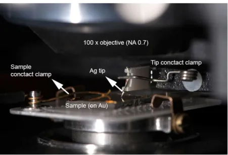
mode TERS. All of the work incorporated in this thesis were conducted on a top-illumination STM-TERS setup.
STM feedback loop. In STM, a bias voltage is applied between the sample surface and a metal tip, when the tip-sample distance is at or below 1 nm, the tunneling current between the tip and sample can be detected. STM imaging can be performed either in a constant current mode by measuring the height with a piezo element or in a constant height mode by measuring the current. The working principle of STM imaging conducted in constant current mode is illustrated in Figure 1.5.
As the tip scans over the sample surface, the topography of the sample is recorded by maintaining the tunneling current at a constant value (setpoint). The tunneling effect between the tip and the sample surface was first demonstrated in 1982 by Gerd Binning and Heinrich Rohrer47, who received the Nobel Prize in Physics for their discovery in 1986.
STM possesses a subnanometer lateral resolution. STM imaging with single atom resolution has been demonstrated.48
Figure 1.5. Scheme to illustrate the working principle of STM imaging performed in a constant current mode. Image credits: Dr. Guillaume Goubert, ETH Zurich.
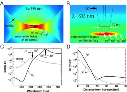
Lightning rod effect / nanoantenna resonance. In TERS, the enhancement mechanisms are similar to those in SERS. According to theoretical calculations, when a Au nanoparticle dimer (Figure 1.6A) is replaced with a Au tip and a Au surface (Figure 1.6B), the maximum EF obtained at the nanogap is predicted to increase by 3 orders of magnitude49. Such a highly intensed enhancement effect in TERS can be rationalized by a combination of the lightning rod effect and an excitation of localized surface plasmons in the gap or the antenna
27 resonance effect50. In TERS, a highly concentrated surface charge is accumulated at the apex of the metal tip under laser irradiation, due to the lightning rod effect.46 This oscillating highly localized surface- charge density is then the source of a highly enhanced and concentrated EM field. Similar to SERS, the tip apex of TERS acts as a nanoantenna to enhance both the excitation and emission processes.
Antenna resonances will be most effective when the tip dimension is matched to the wavelength of incident light (the tip size is not the same as the wavelength of the laser ).46 In Figure1.6, we can compare the case of a Au dimer and a Au tip on a Au surface. It can be seen that due to the coupling between the tip and the surface, the LSPR peak is red- shifted (633 nm), as shown in Figure 1.6C. The EM field is spatially distributed in the gap, and the maximum enhancement is obtained in the hotspot. (Figure 1.6D) Due to the lightning rod effect and nanoantenna resonance, an intense and highly localized electromagnetic field is confined in close proximity to the tip apex, the so-called TERS hotspot, which offers an enhancement up to 107 (experimental result),51 and detection sensitivity down to the single molecule level52-53. Similar to SERS, signal intensity fluctuations of molecules under TERS hotspot are frequently observed. Since there is only one hotspot in TERS, it is easier to see fluctuations in TERS compared to SERS where there are many hotspots. In addition to the metal structure reconstruction (as discussed in SERS hotspot nanogap), a small drift of the tip position relative to the sample also leads to signal fluctuations in the hotspot. Therefore, a TERS hotspot is also a dynamic feature subject to complex ongoing processes. The understanding of the dynamics of TERS hotspots relies on the development of ultrafast imaging techniques with high spatial resolution.
28
Figure 1.6. A. SERS enhancement factor (EF) distribution in the region of the gap (2 nm) between two gold nanoparticles (radii = 30 nm) calculated in the electrostatic approximation with finite-element modeling (for polarization along the vertical axis of the dimer). B. TERS EF distribution in the approximation for a gold tip on top of a gold surface. The tip is separated from the surface by a 2 nm gap (in air). C. Wavelength dependence of the EF at the gap between the dimer shown in A and the gap (axis) between the tip and the surface shown in B. D. the spatial distribution of the EF as a function of distance (on the surface) from the axis. Adapted from Etchegoin et al. Phys.
Chem. Chem. Phys. 2008, 10, 6079–6089 with permission from the PCCP Owner Societies.
Gap-mode TERS using different plasmonic materials. In most of published gap-mode STM-TERS papers, Au has been used as a substrate material. It possesses several advantages, including chemical inertness (very important for TERS measurements in ambient conditions), substrates can be prepared with sufficient flatness and its dielectric constant imaginary part constant ε2 (attributed to losses) is small in the visible optical region.54 Different enhancement in the nanogap will be achieved if different materials are used as TERS substrates. Stadler et al. compared the different enhancement values in
29 gap-mode TERS obtained with different metal substrates.54 The tip material is silver, the material of substrates includes Au, Cu, Ag, Ni, Ti and Mo. The results are shown in Table 1.1. We can see that a nanogap between Au and a silver tip provides the strongest enhancement under irradiation by a red laser, both for the finite-different time domain (FDTD) simulation results and the experimental TERS results. In addition to other advantages mentioned above, gold is the most suitable material used as a substrate for ambient TERS measurements.
Table 1.1 Comparison of the electromagnetic field enhancement in the gap between various metals and a silver tip, using two different simulation techniques and two different experimental approaches. All theoretical values have been normalized to the value of a tip on Au. Experimental values were normalized to the intensity measured on a Au substrate using the same tip
Metal E2 (FDTD)
E4
(FDTD) E2 (FE) TERS (BCB)
TERS (PhS)
Au 1 1 1 1 1
Cu 0.92 0.848 - 0.16 ± 0.11 -
Ag 0.81 0.654 0.559 0.23 ± 0.05 0.77
Ni 0.53 0.281 - 0.07± 0.06 0.72
Ti 0.45 0.199 - 0.12 ± 0.12 -
Mo 0.44 0.194 - 0.11 ± 0.11 -
FDTD, finite difference time domain; FE, finite element; BCB, brilliant cresyl blue.
This table is adapted with permission from Stadler et al. J. Raman Spectrosc. 2013, 44, 227–233.
Spatial resolution. Due to the lightning rod effect and nanoantenna resonances, the enhanced electromagnetic field is highly confined in the vicinity of the TERS tip apex. The size of the electromagnetic field is approximated by the size of the tip apex. Therefore, the spatial resolution is strongly related to the size of the tip apex. In general, when the dimension of the tip decreases, the spatial resolution is
30
improved. However, the field enhancement follows different patterns that also depends on the material of the substrate. When a dielectric substrate (e.g. glass) is used, both the field enhancement and the spatial resolution are improved with decreasing the tip radius (Figure 17A).55 When a coinage metal substrate (e.g., Ag or Au) is used, the field enhancement and spatial resolution follow a different trend due to the strong coupling between the tip and the substrate. For the gap between a Au tip and a Au substrate, the field enhancement increases only moderately when the tip radius increases from 15 to 50 nm.
Further increase of the tip radius does not provide additional enhancement (see Figure 1.7B).56 Therefore, it is important to find the right balance between the sensitivity and spatial resolution for different types of samples.
Figure 1.7. The effect of Au tip radius on the field enhancement and spatial resolution between the full metal tip and different substrate materials: (A) glass substrate. (B) Au substrate. Figure A is adapted with permission from Demming et al. J. Chem. Phys., 2005, 122, 184716. Figure B is adapted with permission from Yang et al. J. Raman Spectrosc. 2009, 40, 1343–1348.
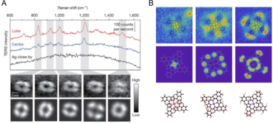
Ultrahigh spatial resolution is a distinct advantage of TERS over SERS. The Dong group52 has already shown the chemical map of a single molecule using TERS at ultrahigh vacuum (UHV) and cryogenetic conditions.(Figure 1.8A) Very recently, the Apkarian group53 pushed the limit even down to the atomic level (visualization
31 of the vibrational modes in a single molecule), again with the use of UHV TERS.(Figure 1.8B) The subnanometer (Å) spatial resolution of TERS seems in contradiction with the statement above that the spatial resolution is close to the diameter of the tip. It is important to note that the apex is not an atomically flat surface, but a very rough surface with lots of small particles or protrusions. Thus, such a high spatial resolution is due to the confinement of light in the small region, so- called picocavities57. Benz et al.57 used single Au NP SERS on a gold film with a self-assembled monolayer of biphenyl-4-thiol. They observed several transient lines in the Raman spectra intermittently, which is due to the highly enhanced EM field induced in picocavities. The atomic protrusions can be stable at cryogenic conditions, but they diffuse quickly at room temperature. This makes the TERS mapping with ultra high spatial resolution difficult to reproduce at ambient conditions.
Figure 1.8. TERS mapping of porphyrins with sub-nanometer spatial resolution a.
meso-tetrakis(3,5-di-tertiarybutylphenyl)-porphyrin (H2TBPP) porphyrin on Ag (111).
B. Co(II)-tetraphenyl porphyrin on Cu (100). Figure A is adapted with permission from Zhang, et al. Nature 2013, 498, 82-86. Figure B is adapted with permission from Lee et al, Nature 2019, 568, 78-82.
32
The highest spatial resolution in ambient TERS so far reported is around 2-3 nm,58-59 depending on the system. Compared to UHV TERS, there are several intrinsic disadvantages for ambient TERS: 1. The tip is easily degraded (especially for Ag tip) or contaminated, and the sample is also easily contaminated. 2. Thermal drift of either the tip or the sample during measurements is unavoidable. 3. The morphology of the tip at the hotspot is constantly changing during measurements.
While recording a TERS map, it usually happens that the tip loses the enhancement activity after/while mapping, sometimes the tip will have stronger enhancement than before the mapping started. The reproducibility of TERS is another important issue that needs to be considered. A lot of factors influence the TERS results, such as tip size and geometry (each tip has unique structure at the tip apex), the probed sample area (when we change to a new tip, the new tip will be located on a different sample area from before), the stability of the distance between the tip and the sample, and so on. Therefore, in general it is difficult to reproduce TERS mapping results.
Surface selection rules. In TERS, in addition to the normal Raman selection rules, surface selection rules must also be considered. The surface selection rule for IR is explained in the following: When a molecule absorbed on a metal surface vibrates, it creates a dipole, which then induces an image dipole within the substrate due to the high electron mobility in metals. It follows that the vibration perpendicular to the metal surface is enhanced, whereas the one parallel to the metal surface is canceled by its instantaneous image,60 as shown in Figure 1.9. Although the polarizability change of molecules is the key to induce Raman scattering, the surface selection rule for IR can also be applied to Raman spectroscopy. In confocal Raman spectroscopy, all possible Raman-active vibrational modes of the molecules can be excited. In TERS the sample molecules are placed on a metal surface. Therefore, only those Raman modes containing
33 considerable out-of-plane vibrational components and allowing for efficient enhancement by axial plasmonic fields are visible in TERS.61
Figure 1.9. Schematic illustration of the orientation selection rule for surface dipole.
The adsorbed dipole parallel to the metal surface will be canceled by the image dipole.
However, the dipole perpendicular to the metal surface will be enhanced by the image dipole instead.
1.3 Interface reactions
Liquid-gas, solid–gas, and solid–liquid interfaces play the most important roles in photochemistry, heterogeneous catalysis, and electrochemistry. The molecules present in gas or liquid phase as reactants, products, solvents or electrolytes in the region close to the surface, form a complex interfacial region.44 Various complex processes, including reactions, may occur in this region. Here, we introduce three different types of interface reactions, including polymerization, photoisomerization and catalytic hydrogenation.
1.3.1 Polymerization
To understand interfacial polymerization, we need to first introduce a new type of polymers, namely two-dimensional polymers (2D
34
polymers). 2D polymers62-63 are one monomer unit-thin, covalently linked networks with long-range order along two orthogonal directions, which have aroused intense attention in recent years due to their potential applications in electronics, catalysis and sensing64-66. Since 2D polymers are obtained based on the polymerization among monomer molecules which must be equipped with at least three functionalities for network formation, pores are usually contained in the structure of 2D polymers. The size of pores can be tuned by designing different monomer structure.
There are several different ways to synthesize 2D polymers. One way is through the single-crystal method67-68, which requires an exfoliation step to obtain monolayer sheets. The exfoliation methods include mechanical exfoliation and solvent-phase exfoliation.67-69 Up to date, exfoliation of single crystals remains problematic.70 The maximally achievable sheet size is limited by the size of single-crystal. So far the largest single sheet fabricated from the single-crystal method is in the range of a few micrometers.71-72 Another way is through the interfacial synthesis, i. e., at either an air/water or a liquid/liquid interface.39, 70, 73- 74 The monomers are confined in two dimensions at the interface prior to or during polymerization. Hence, the reaction occurs at the interface.
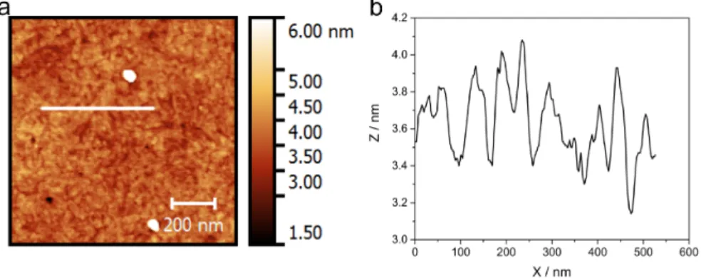
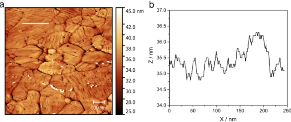
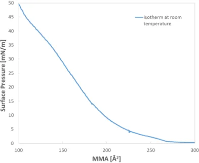
The synthesis of 2D polymers at a liquid/liquid interface is usually carried out in a beaker. In contrast, the air/water approach is usually performed on a Langmuir-Blodgett (LB) trough. A LB trough is capable of applying a defined surface pressure and can be coupled with analytical equipment, such as a Brewster angle microscope (BAM)75-76 or fiber optics for in-situ fluorescence spectroscopy77. Another advantage of this method is that it provides 2D polymer sheets with large lateral size. The amphiphilic monomer molecules are spread at the air/water interface, the monolayer packing of monomers forms when an appropriate surface pressure is applied. Subsequently, the polymerization is performed at the interface. The thickness of the layer can then be determined with AFM imaging after transfer onto a
35 substrate. Therefore, the layers of molecules can be precisely controlled in this method, which is usually not the case in the liquid/liquid interface approach. The final way to create 2D polymers is to perform polymerization directly on solid substrates78-79. The differences between the air/water interface and solid substrates are as follows: 1. the ease of the lateral mobility of monomers; 2. the compliance of the aqueous phase; 3. the absence or presence of fixed terraces and grain boundaries. Under the same experimental conditions, the conversion of polymerization achieved at air/water interface is therefore higher than that achieved on solid substrates.
To date, various polymerization reactions have been used for the synthesis of 2D polymers at air/water or liquid/liquid interfaces.63, 70 Among them, anthracene dimerization reaction and condensation reaction between amine and carbonyl groups are two frequently used reactions, as demonstrated by several research groups.66, 73, 80-81 The detailed discussion about these two reactions is as follows:
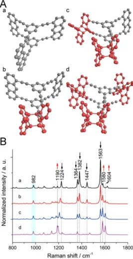
Anthracene dimerization. As shown in Figure 1.10 A and B, the monomers 173 and 282 are both amphiphilic molecules incorporating anthracene groups. When a dense monolayer of monomer is formed at the air/water interface with the anthracene units face-to-face (ftf), anthracene units of these monomers are subjected to a [4+4]- cycloaddition dimerization between pairs of these units upon UV irradiation (λ = 365 nm). This reaction is in principle reversible. When the sample is irradiated at 254 nm or heated to 200 oC, the back reaction will occur, as shown in Figure 1.10C. Especially, when the dimerization reaction takes place in air, side-reactions, such as photooxidation83, may occur sometimes.
36
Figure 1.10. A /B. Monomers used at the air/water interface for the synthesis of 2D polymers through anthracene dimerization reaction. C. The photochemical dimerization reaction between two anthracenes. The dimerization reaction is triggered by light irradiation at 365 nm and the back reaction is triggered by light irradiation at 254 nm or heating. Figure A is adapted with permission from Müller et al.
Angew. Chem. Int. Ed. 2017, 129, 15464-15468. Figure B is adapted with permission from Opilik et al. ACS Nano 2015, 9, 4252-4259. Copyright (2015) American Chemical Society.
Condensation reaction between amine and carbonyl groups. In this strategy, two monomers containing amine and carbonyl groups, respectively, (monomers 3 and 480 or 5 and 666, as shown in Figure 1.11) are co-spread at the interface with a 1:1 stoichiometry per functional group. These two groups can form imine bonds in a reversible, acid catalyzed fashion. It is worthy to note that the three hexyl chains in 4 are an essential structural feature because they help form homogeneous monolayers.
Figure 1.11. Monomers used at the air/water interface for the synthesis of 2D polymers relying on Shiff-base chemistry.
37 Regarding the synthesis of 2D polymers, there are several key questions: 1. When is the polymerization reaction complete? 2. What is the nature of networks formed among monomers? 3. Are there defects within the sheet? The characterization of obtained sheets is critical and challenging, since the amount of 2D polymer is extremely small, usually below 1 µg. Hence, a lot of routine analytical methods, for example NMR spectroscopy and XRD, are inapplicable. TERS is suitable for the analysis of 2D polymers, thanks to the high sensitivity and high spatial resolution. In Chapter 3, we show how TERS was used for the structural analysis of covalent monolayers synthesized through anthracene dimerization at air/water interface and on Au (111).
1.3.2 Photoisomerization
Photoisomerization is a molecular transformation in which a structural change of the molecule between two isomers is triggered by irradiation with light. The isomerization of switchable molecules can also be induced mechanically84, thermally85, or through the application of voltage or current pulses86. Here, we only focus the discussion on photoisomerization. Conformational changes of functional molecules, such as photoisomerization, are a fundamental concept in nature, a lot of complex biological processes involve photoisomerization.87 An example is the light-induced cis-to-trans-isomerization of retinal, which plays an important role in vision88. Such switching processes represent an attractive strategy for the development of new technologies. Molecular switches have received a lot of attention, due to their potential applications in molecular electronics and high- density data storage.89-91
There are two major classes of photoisomerization reactions. The first type is trans/cis or Z/E isomerization. Representative photo switches belonging to this category are azobenzene92 and hydrazone93. The second type involves ring closing/opening transition, a typical
38
photo switch belonging to this category is diarylethene94. Here we only focus our attention on two kinds of photo switches from the first class:
azobenzene and its derivatives, and hydrazone.
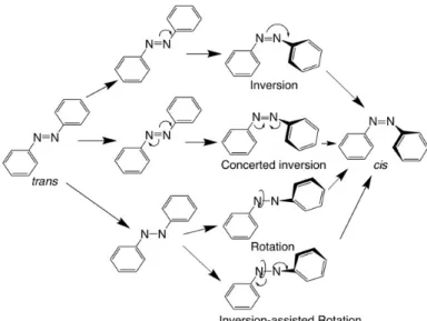
Azobenzene. Azobenzenes are among the most thoroughly investigated photo switches. As shown in Figure 1.12A, azobenzene undergoes trans-to-cis isomerization when irradiated with light at a wavelength of 365 nm. The reverse cis-to-trans isomerization can be driven by light (λ = 450 nm) or occur thermally in the dark due to the greater thermodynamic stability of the trans isomer.92, 95 Trans- azobenzene undergoes trans-to-cis isomerization following both S0→ S1 (nπ*) and S0→ S2 (ππ*) excitation. Similarly, cis-azobenzene can be changed to the trans state by exciting into the S1 or S2 state, as shown in Figure 1.12B.96 The switching mechanism of azobenzene in solution is well understood. There are four mechanisms proposed as possible pathways for azobenzene photoisomerization, including inversion, concerted inversion, rotation and inversion-assisted rotation,97-100 as shown in Figure 1.13. The pathway for azobenzene photoisomerization is a complex topic. The pathway deduced from the experimental result-
Figure 1.12. A. Photoisomerization of azobenzene. B. UV absorption spectra of azobenzene thiol before and after irradiation at a wavelength of 365 nm. The S0→ S1
transition appears as a weak band at 440 nm and S0→ S2 transition appears as a band at around 330 nm.
39 s sometimes is contrary to that predicted by computational simulations. For example, resonance Raman intensity analysis indicates that the isomerization pathway most likely involves inversion.101 However, dynamic simulations suggest that isomerization occurs via inversion-assisted rotation.102-103 In solution, the quantum yield of isomerization is affected by different factors, including irradiation wavelength, polarity and viscosity of solvent, temperature, substituents of azobenzene, etc.92
When azobenzene and its derivatives are adsorbed on a metal surface, the isomerization occurs at the interface, in which switching mechanism is quite different from that in solution. In contrast to the direct molecular excitation in solution, Tegeder et al. proposed a substrate-mediated charge transfer mechanism for the isomerization of 3,3’,5,5’-tetra-tert-butyl-azobenzene (TBA) physically absorbed on Au (111) studied by two-photon photoemission spectroscopy.104 For azobenzene derivatives chemisorbed on a metal surface, the reversible isomerization has been studied by SERS105, UHV-TERS106 and STM38, etc. However, a deep understanding of the isomerization behavior on a molecular level has not yet been achieved. For instance, is there any relationship between the metal surface structure and isomerization rate? To answer this question, we need an analytical tool, such as TERS which provides molecular information with high spatial resolution. In Chapter 4, we will present a thorough study of isomerization behavior of an azobenzene thiol self-assembled monolayer (SAM) on Au using TERS.