of Fe 3 − x Co x O 4 with x = 0, 0.1, 0.5, 1 and their properties
Inaugural - Dissertation zur
Erlangung des Doktorgrades
der Mathematisch-Naturwissenschaftlichen Fakultät der Universität zu Köln
vorgelegt von
Akfiny Hasdi Aimon
aus Padang, Indonesien
Köln 2014
Tag der mündlichen Prüfung: 21.10.2014
1 Introduction 1
1.1 Tunability of physical properties in ferrites thin films . . . . 1
1.2 Structure and properties . . . . 4
1.2.1 Magnetite (Fe
3O
4) . . . . 4
1.2.2 Cobalt Ferrite (Fe
2CoO
4) . . . . 6
1.3 Scope of this thesis . . . . 7
2 Experimental Techniques and Set-up 9 2.1 Thin films growth . . . . 10
2.1.1 Epitaxy . . . . 10
2.1.2 Molecular Beam Epitaxy (MBE) . . . . 12
2.2 RHEED and LEED . . . . 14
2.2.1 RHEED . . . . 14
2.2.2 LEED . . . . 17
2.3 X-Ray Di ff raction . . . . 19
2.4 Spectroscopy . . . . 21
2.4.1 XPS . . . . 23
2.4.2 XAS . . . . 25
2.5 Magnetometry (SQUID) . . . . 28
3 Epitaxial growth and structural characterization of Fe
3−xCo
xO
4films 31 3.1 Introduction . . . . 31
3.2 Fe
3−xCo
xO
4thin films growth . . . . 32
3.2.1 Substrate preparation . . . . 32
3.2.2 Growth conditions . . . . 34
3.3 Structural characterization . . . . 35
3.3.1 In-situ RHEED and LEED . . . . 35
3.3.2 Ex-situ XRD . . . . 41
4 X-ray Photoemission study of Fe
3−xCo
xO
4Thin Films 47 4.1 Introduction . . . . 47
4.2 Experiment . . . . 48
4.3 Results and Discussion . . . . 48
4.3.1 Core Levels . . . . 49
4.3.2 Valence band . . . . 54
5 Initial study of sites occupation on Fe
3−xCo
xO
4films by X-ray Absorp-
tion (XAS) 59
5.1 Introduction . . . . 59
5.2 Experiment . . . . 60
5.3 Results . . . . 60
5.3.1 Substitution dependence . . . . 62
5.3.2 Thickness dependence . . . . 64
6 Magnetic study of Fe
3−xCo
xO
4films 69 6.1 Introduction . . . . 69
6.2 Experimental . . . . 70
6.3 Results . . . . 71
6.3.1 Bulk magnetic properties of Fe
3−xCo
xO
4films . . . . 71 6.3.2 Magnetic anisotropy induced by strain in Fe
2CoO
4films . 74
7 Summary 81
Bibliography 85
Abstract 93
Kurzzusammenfassung 95
Acknowledgement 97
Erklärung 99
Curriculum vitae 101
Introduction
1.1 Tunability of physical properties in ferrites thin films
During the past decades, transition metal (TM) oxide compounds have attracted growing research interest because of their promising applications in microelec- tronic, and microwave devices as well as sensitive sensors. In particular, these materials display a variety of unique magnetic and electronic properties such as magnetoresistance (MR), magnetoelectric and magneto-optic e ff ects, as well as others that result in their prospective applications for data storage and switching devices involving actuators and transducers [1–5]. These properties are now com- monly understood to have their main origin in the strongly correlated 3d electrons occupying the incomplete 3d orbitals in the transition metal cations.
For advanced applications, it is often desirable to have materials with mag- netic properties which can be e ff ectively controlled by external parameters such as applied electric filed, elastic stress, or light. In this respect, ferrites, Fe
3O
4(mag- netite), is a highly promising candidate. Firstly, it has a high Curie temperature of T
c≃ 860 K and according to band-structure calculation, it is expected to be half- metal[6–9]. Secondly, recent experiments show that the MR value of Fe
3O
4can be enhanced by Mn substitution [10]. Thirdly, it was demonstrated that the magnetic anisotropy of Fe
3O
4can be tuned by elastic stress imposed by a piezoelectric actu- ator. Moreover, this compound is known to exist in either the normal or the inverse spinel structure [11]. The degree of the two structure mixing can be quantified by an inversion parameter, λ , that is the fraction of divalent cations that reside on the octahedral sites ( λ= 0 for normal spinel and 1 for inverse spinel). It is known that even a small changes in λ can lead to significant changes in magnetization [12].
The physical properties of a magnetite can also be tuned through small changes
in chemical composition (substitution) in addition to strain e ff ect. For examples
both the electronic and magnetic properties of Fe
3O
4can be nicely tailored in solid
solution system of Fe
3−xM
xO
4(M = Mn, Co, Ni and Zn) by proper variation of the
substitution concentration (x) [13–17]. Besides, external pressure and temperature
can also be employed to induce remarkable changes in the electronic structure and
properties. It was shown in a nanocrystalline sintered cobalt ferrite powder, that a
large magnetostriction and coupling coe ffi cient were obtained at room temperature
for sample pressurized at 8 MPa. Further, magnetic annealing of the sample at 300
oC in a magnetic field of 0.5 T exhibited an enhanced magnetostriction and coupling coe ffi cient [18].
In addition to the importance of thin films for device applications, it is well known that thin films can also produce novel functionalities in the associated ma- terials since their physical parameters can be modified by their structure changes in- duced by substitution, thickness, and strains. Recently, doped magnetite (Fe
3−xM
xO
4, with M = Mn, Co, Ni and Zn) in thin films forms were extensively studied to inves- tigate the substitution e ff ect on the structural and magnetic properties of magnetite, and to exploit new functional materials [19–26]. They show that the degree of substitution can control the conductivity of spinel ferrite. The resistivity and den- sity of states near the Fermi energy of Fe
3−xM
xO
4thin films behaves systematically upon substitution. Moreover, the magnetic structure of Fe
3−xM
xO
4have shown that the magnetic moment behaves nonlinearly with the substitution agent and does not obey Neel’s theory of ferrimagnetism [19–25]. This has been attributed to changes in the strength of the magnetic interactions among the di ff erent cations.
Apart from the substitution e ff ect, the thin films properties can also be tuned by the films thickness. It has been reported by Lisfi et al. [27] that the spin reorienta- tion in Fe
2CoO
4thin films epitaxially grown along the (100) axis of MgO substrate can be a ff ected by structural transition in the film from a tetragonal to cubic sym- metry induced by the films thickness variation. Another evident is also reported by Moyer et al. [28] that the e ff ect of film thickness on magnetic properties of Fe
3−xCo
xO
4films shown a superparamagnetic state in ultrathin sample.
The strain e ff ect as a consequence of the substrates used has been shown to provide the possibility for inducing ferroelectric (FE) and ferromagnetic (FM) cou- pling leading to more e ffi cient electric-magnetic field controllability of the related device operation [29, 30]. Meanwhile, a number of studies have been carried out in order to understand the correlation between the magnetic behaviors and the strain of Fe
2CoO
4thin films. For examples, Liu et al. has reported their studies on Fe
2CoO
4films grown on glass and single-crystal quartz substrates by sputtering method [31].
They found that the high coercivity mechanism is associated with nanocrystalline
structure, in particular the presence of relatively large residual strain in the sam-
ple. Meanwhile, Huang et al. also revealed that the strong magnetic anisotropy is
highly dependent on the lattice-mismatch induced strain in Fe
2CoO
4thin films epi-
taxially grown on SrTiO
3and MgO (001) [32]. In a most recent report by Moyer
et al. It was shown that λ can be increased and decreased by the application of
compressive and tensile epitaxial strains. These changes result in the changes of
the transition metal cations distribution in the A and B lattice sites (to be explained
later in section 1.2.1) as well as the film conductivity [33]. Taken all together,
in view of those interesting versatile and tunable properties of magnetite, the thin
films of this material has become a focus of recent research activities.
It is worth noting, that instead of applying hydrostatic pressure on bulk sample which is limited to producing compressive strain only, epitaxial strain can pro- duce both compression and tensile strains to a thin film sample. This is achieved by simply choosing the sign of the lattice mismatch between substrate and films.
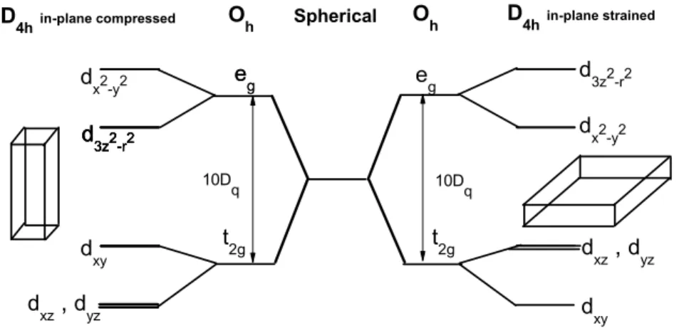
Moreover, a 2% of epitaxial strain between the substrate and the film is equivalent to the e ff ect of 10GPa hydrostatic pressure. It should be noted that a strain of a few percents can be easily realized by epitaxial growth as long as the thickness of the layer is smaller than the critical thickness for spontaneous dislocation. The additional advantage of epitaxial strain is the possibility to expand or compress the crystal structure along the direction perpendicular to the surface which can not be achieved by hydrostatic pressure. Thus, the epitaxial growth process can deform the unit cell of the film from cubic into tetragonal symmetry, which will in turn give rise to changes of certain physical properties of a thin film [34, 35]. An exam- ple presents in figure 1.1 which is associated to a simple schematic diagram of the energy levels due to tetragonal distortion in octahedral symmetry.
10D
q 10D
q e
g
O h O
h
Spherical D
4h
in-plane strained D
4h
in-plane compressed
t 2g t
2g
e g e
g
d xz
, d yz
d xz
, d yz
d xy d
xy d
x 2
-y 2
d 3z
2
-r 2
d 3z
2
-r 2
d x
2
-y 2 d
3z 2
-r 2 d
3z 2
-r 2 d
3z 2
-r 2
Figure 1.1: The d energy levels diagram for a transition metal atom in a tetragonal distorted octahedra.
However in this study, it will only focus on the study of the influences of Co- substitution and epitaxial strain on the physical properties of Fe
3−xCo
xO
4thin films.
In addition, the thickness dependent of Fe
3−xCo
xO
4thin films is also studied to
figure out the cations distribution behavior in this compound. In the next section, a
brief introduction will be given on the most relevant bulk properties of Fe
3O
4and
Fe
2CoO
4systems.
1.2 Structure and properties
1.2.1 Magnetite (Fe
3O
4)
O 2- Fe
3+
/ Fe 2+
Fe 3+
Figure 1.2: The inverse spinel structure of Fe
2CoO
4. It consists of an fcc network of oxygen anions (small red spheres) with cations occupying di ff erent interstitial sites of the fcc lattice, resulting in tetrahedrally coordinated A-sites (blue) and oc- tahedrally coordinated B-sites (green). Picture has been generated using Diamond.
Prior to detailed discussion of the structure and properties of Cobalt Ferrite (Fe
2CoO
4), it is helpful to give a brief introduction recalling what are commonly known about Magnetite (Fe
3O
4) which is the mother compound of the ferrites. The Fe
3O
4compound is known to have the inverse spinel crystal structure with space group Fd ¯3m as sketched in figure 1.2. It has a slightly distorted cubic close packed lattice of O
2−anions as its basis. The lattice constant of Fe
3O
4is 8.394 Å [36]. The Fe
3O
4is among the most interesting iron oxides due to the presence of Fe cations in two valence states; namely the ferrous Fe
2+and the ferric Fe
3+ions. The Fe
2+ions are known to be located in the octahedral (B) sites only, while the Fe
3+are found to reside in both octahedral (B) sites and tetrahedral (A) sites. A simple schematic picture of the electron configuration in this compound is shown in figure 1.3.
It is well known that in each lattice site, the spins of Fe
3+and Fe
2+in the
B sites are aligned in ferromagnetic order. Often this is explained in term of a
double exchange mechanism as shown in figure 1.4. However, it is the strong
antiferromagnetic superexchange coupling between the A sites and the B sites that
Fe 2+
(d 6
)
S = 2
B site Fe
3+
(d 5
)
S = 5/2
B site Fe
3+
(d 5
)
S = 5/2
A site e
g t
2g
e g t
2g t
2g t
2g
t 2g t
2g e
g e
g
t 2g t
2g e
g e
g
t 2g t
2g e
g e
g
Figure 1.3: a) The electron configurations of Fe
3+in tetrahedral site and those of Fe
3+and Fe
2+in octahedral site. All the tetrahedral and octahedral sites are high spin state (weak crystal field).
makes the B sites to have the same spin alignment. As a result the total spins of the system arises from the sole configuration Fe
2+leading to a net magnetic moment of 4 µ
Bper formula unit of Fe
3O
4. Consequently, the Fe
3O
4is e ff ectively a ferrimagnetic material with a Curie temperature T
Cof 858 K.
e g
Fe 2+
(d 6
) Fe
3+
(d 5
) t
2g
Figure 1.4: The double-exchange mechanism giving ferromagnetic coupling be- tween ions participating in Fe
2+/ Fe
3+electron transfer.
At room temperature, Fe
3O
4is known to exhibit reasonable conductivity due to the hopping of electrons between the Fe
2+and Fe
3+ions in the octahedral strings.
The ferromagnetic alignment of neighboring ions is shown to maintain the high-
spin arrangement of electrons on both the donating and the receiving ion. When
the compound is cooled down through the Verwey transition temperature T
Vof 124
K in bulk Fe
3O
4crystal, the electron hopping freezes out, leading to an ordered
array of Fe
2+and Fe
3+ions and an increase of resistivity by over two orders of
magnitude [37]. This transition is also marked by the concurrent change of the
crystal structure from cubic to monoclinic, along with the changes of orbital and
charge orders.
1.2.2 Cobalt Ferrite (Fe
2CoO
4)
One of the most important attributes or advantages of ferrites is the very high de- gree of their compositional variability. Among the most well known compounds is Cobalt Ferrite (Fe
2CoO
4). The Fe
2CoO
4is a hard magnetic material with high de- gree of magnetic anisotropy and magnetostriction. The unique magnetic properties of this material can be understood from its structural and electronic configuration.
The study of magnetism in Fe
2CoO
4has recently become a focus of material re- search due to its promising applications for oxide based magnetoelectric devices, in particular in nanocrystalline form [18].
A previous Neutron di ff raction measurement on powder Fe
2CoO
4sample con- firmed that the Fe
2CoO
4has inverse spinel structure [38]. Specifically, the Co
2+ions were found to occupy the B site replacing the Fe
2+whereas the Fe
3+ions were shown to be distributed equally in the A and B sites. A unit cell of Fe
2CoO
4is also shown to have a face-centered cubic (fcc) structure with the lattice parameter (a
0) of 8.3765 Å. This is perceptibly shorter than that for Fe
3O
4(8.394Å) mention in previous subsection. Comparing this parameters of Fe
3O
4and Fe
2CoO
4one read- ily concludes that the structure of the Co-doped crystal has become compressed due to the presence Co atoms in the structure.
Co 2+
(d 7
)
S = 3/2
B site Fe
3+
(d 5
)
S = 5/2
B site Fe
3+
(d 5
)
S = 5/2
A site e
g t
2g
e g t
2g t
2g t
2g
t 2g t
2g e
g e
g
t 2g t
2g e
g e
g
t 2g t
2g e
g e
g
Figure 1.5: The electron configurations of Fe
3+in tetrahedral site and those of Fe
3+and Co
2+in octahedral site. All the tetrahedral and octahedral sites are high spin state (weak crystal field).
The electron configuration of Fe
2CoO
4is shown in figure 1.5. Recalling that in the case of Fe
3O
4the eight Fe
3+ions in tetrahedral sites are aligned antiferromag- netically with respect to the remaining eight Fe
3+ions in octahedral sites via su- perexchange interactions mediated by oxygen ions. Thus the uncompensated Co
2+ions which have three unpaired electrons in their d-orbitals would give a theoretical
saturated magnetization of 3 µ
B. This turns out to be smaller than the experimen-
tal value (3.35 µ
Bat 300K) given by Neutron data [38]. The discrepancy between
the theoretical and experimental values could be attributed to two factors. Firstly,
the calculation was done by neglecting the contribution from the orbital motion of electrons. Secondly, the Fe
3+moments in the A and B sites were assumed to be aligned in perfect anti-parallel directions, while in reality they may be canted. In addition, the distribution of the cations in di ff erent sites may not be as perfect as assumed.
Still another interesting e ff ect of Co-substitution in Fe
3O
4is worthwhile to be presented in this connection. As mentioned earlier, the Fe
3O
4is known to be con- ductive magnetic material at room temperature. It was shown however that adding the Co ions in the compound can increase the resistivity of the Fe
2CoO
4up to 10
7Ω cm [39]. This drastic change may partly due to the e ff ective replacement of Fe
2+by Co
2+which has a di ff erent electronic structure from the Fe
2+ions.
d x
2
-y 2
d 3z
2
-r 2
d xy
d xz
, d yz
Co 2+
(d 7
)
Octahedral
(O h
)
Co 2+
(d 7
)
Tetragonal
(D 4h
) t
2g t
2g e
g e
g
Figure 1.6: The change in the Co
2+orbital energy scheme and electron configura- tion induced by J-T distortion.
Besides, as described early, Co-substitution is also expected to induce struc- tural change which will intern modify overall electronic structure. The presence of orbital degree of freedom on the Co
2+octahedral site is expected to induce a weak Jhan-Teller (J-T) distortion resulting in the lowering of the octahedral symmetry to tetragonal symmetry as shown in figure 1.6, along with the resulted orbital energy split. Taken together, those changes may no longer provides the favorable condition for the electron hopping mechanism.
1.3 Scope of this thesis
This thesis is devoted to the investigation of a number of structural, spectroscopic,
electric and magnetic properties of the Fe
3−xCo
xO
4thin films for varying x (x = 0,
0.1, 0.5, 1). The Molecular Beam Epitaxy (MBE) method was employed to prepare
the epitaxial and monocrystalline thin films. A main concern of this thesis work
is to explore the influences of the epitaxy strain on the physical properties of the films. The use of epitaxial strain is expected to modify the site occupation of the cations and the orbital ordering as well as the influences of those modification on the physical properties. For these investigation the quality and the structure of the resulted thin film are characterized by Reflection High Energy Electron Di ff rac- tion (RHEED), Low Energy Electron Di ff raction (LEED) and X-Ray Di ff raction (XRD). The spectroscopy study are performed by means of X-Ray Photoemission Spectroscopy (XPS) and X-Ray Absorption Spectroscopy (XAS) measurements for the purpose of determining the electron configurations of the cations. Addition- ally, the SQUID measurements are carried out to study the magnetic properties of the films.
Aside of the introductory chapter, the rest of this thesis will be organized as follows. In the next chapter (chapter 2), descriptions will be presented on the ex- perimental techniques employed for sample preparation as well as the sample char- acterizations and physical properties measurements. Specifically, the MBE method will be explain together with the set-up used for the growth of the films. Next, the RHEED, LEED, and XPS method will be describe for in-situ measurements, while the XRD, SQUID and XAS techniques will be explain for ex-situ characterizations.
Chapter 3 contains the detailed description of the growth procedure for the Fe
3−xCo
xO
4x = 0, 0.1, 0.5, 1 thin films on di ff erent substrates, namely MgO (100), MgAl
2O
4(100), and SrTiO
3(100). Also presented in this chapter is the explanation of the quality verification steps taken in the entire process of the films growth using RHEED, LEED and XRD measurements.
In chapter 4, it will present the result of the XPS measurement and the associ- ated analysis of the electronic structures. The evidence of the Co valency revealed by the Co
2pcore level spectra is presented as the result of the XPS analysis. This is followed by the discussion of the e ff ect of Co-substitution in the Fe
2pand O
1score level spectra. Based on the valence band spectra, one may deduce the e ff ect of the Co-substitution on the electronic properties.
Further study on the electronic spectroscopy of Fe
3−xCo
xO
4will be described in chapter 5. Here it will discuss the XAS spectra unraveling the ionic valencies and the local symmetry of the cations due the present of the Co atoms. The discussion on the thickness e ff ect on the valency and the site occupation will also be given.
In chapter 6, we report the magnetic properties of the Fe
3−xCo
xO
4films based
on the SQUID measurement of the hysteresis loop characteristics. Further analysis
of this data provide the information of the rotation of the magnetic easy axis due
to strain e ff ect. Moreover, the X-Ray Linear Dichroism (XLD) measurement will
be shown to substantiate the study on strain e ff ect related to the use of di ff erent
substrate by proving the information of the spin orientation and also orbital occu-
pancy as a function of the epitaxial strain. Finally, in chapter 7, it will summarize
the work on this thesis.
Experimental Techniques and Set-up
This chapter delivers the experimental technique that was used for this thesis work.
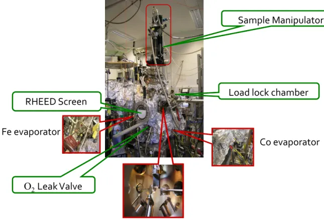
It will introduce the basic concept and the experimental set-up. Figure 2.1 shows the chamber that was used to grow thin film samples for this thesis. The MBE chamber was directly connected to LEED and XPS chamber (not shown in the figure) so that the freshly prepared samples could be transferred and measured all in vacuo, thereby assuring the cleanliness and reliability of the data.
O 2
Leak Valve RHEED Screen
Sample Manipulator
Load lock chamber
Fe evaporator
Co evaporator
Figure 2.1: MBE set-up for film growth at the experimental Lab. in Köln.
2.1 Thin films growth
2.1.1 Epitaxy
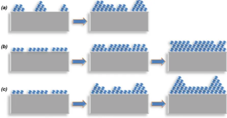
Figure 2.2: Schematic illustration of (a) nearly perfectly lattice matched, (b) strained, and (c) relaxed heteroepitaxial film growth. This figure is retrieved from Ref. [40].
Epitaxy is the extended single-crystal film formation on top of a crystalline
substrate. There are two general types of epitaxy; homoepitaxy and heteroepi-
taxy. As the name implies, the homoepitaxy is the thin films growth on the same
substrate material, for instance doped-Si on a Si substrate. It can produce high
quality film, free of defects, but have a di ff erent substitution or functional nature
than the substrate. The other type of epitaxy, heteroepitaxy, is the case where the
film and substrate are di ff erent materials, but have similar structures that help to
guide the film growth. Figure 2.2 illustrates the di ff erences between these two epi-
taxy. Figure 2.2a is typical growth of homoepitaxy, while figure 2.2b and c are
the heteroepitaxy type. As shown in figure 2.2a, epitaxy can be succeeded if the
film material is exactly the same as the substrate or they are di ff erent materials that
have very small di ff erence in lattice parameter and interfaces so that it only gives
little disturbance of the structure across the interfaces. However, if the film and
substrate have di ff erent materials and also di ff erent lattice mismatch, it is possible
to form one of two types of interfaces as sketched in figure 2.2b and c. Figure 2.2b
is so-called strained-layer epitaxy for the film which has similar structure and lat-
tice mismatch with the substrate (i.e., perovskite on perovskite). The last type of
growth is relaxed epitaxy as shown in figure 2.2c. In this type of growth the film
has a larger lattice mismatch with the substrate and even di ff erent crystal struc-
ture. As a consequence, the film turns out to have relatively quick relaxation to its bulk structure through the formation of defect, like dislocation, that accommodates interfacial strain in the system and lead to a relaxed film.
Figure 2.3: Illustration of basic growth modes: (a) Volmer-Weber (island), (b) Frank-Van der Merwe (layer-by-layer), and (c) Stranski-Krastanov. This figure is retrieved from Ref. [40].
In an epitaxy process, there are three typical modes to grow a thin film: (1)
Volmer-Weber or island growth, (2) Frank-Van der Merwe or layer by layer growth,
and (3) Stranski-Krastanov growth. These growth mechanisms are illustrated in
figure 2.3. The Volmer-Weber or island growth (figure 2.3a) arises when the small-
est stable clusters nucleate on the substrate and grow into three-dimensional island
features. This growth behavior can be explained in the simple picture that the evap-
orated atoms or molecules have strongly bonded to each other than to the substrate
material. This can be found for di ff erent film and substrate materials, for example
metal grown on oxide substrates. However, the opposite characteristic is revealed
by Frank-Van der Merwe or layer by layer growth (figure 2.3b). It takes place
when the extension of the smallest nucleus occurs in two dimensions resulting in
the formation of planar sheets. In this type of growth mode the evaporated atoms
or molecules are more strongly bonded to the substrate than each other. Therefore,
each layer is progressively less strongly bonded than the previous layer. This be-
havior will remain continuously until it reachs the bulk bonding strength. This is
typically growth mode of semiconductors and oxide materials. The final growth
mode is the Stranski-Krastanov growth (figure 2.3c) which is a combination of the
layer-by-layer and island growth. In this type of growth, the film starts to grow
in a layer-by-layer fashion. After several monolayers this type of growth is not
energetically favorable, therefore it starts to change into islands mode. This type
of growth is fairly common in a number of metal-metal and metal-semiconductor systems.
2.1.2 Molecular Beam Epitaxy (MBE)
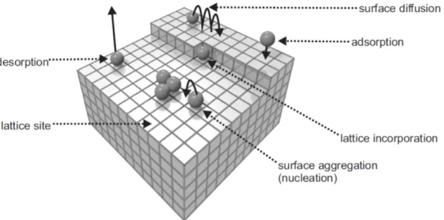
Figure 2.4: Schematic illustration of the fundamental processes for thin film depo- sition. This figure is retrieved from Ref. [41]
Molecular Beam Epitaxy is a thin film growth technique in which the mate-
rials in the form of molecular or atomic beams condensate at a heated substrate
surface under certain growth conditions. The MBE growth mechanism involves
three steps; the production of molecular beams, the transport of molecular beams
to the substrate and the deposition of the molecular beams onto the substrate. The
molecular beam can be generated by the e ff usion cell (Knudsen cell) or electron
beam (e-beam) evaporators. In an e ff usion cell the material is evaporated from
crucible that is surrounded by a heating coil. For materials that require a (very)
high temperature for evaporation, it can be used the e-beam evaporator. In this
type of evaporator, the evaporant can be either a rod or lie in a crucible, and then
the electrons are emitted from a circular filament that is positioned slightly above
the evaporant. Typically, the MBE set-up is in Ultra High Vacuum (UHV) con-
ditions which are in the 10
−9− 10
−11mbar range, compatible with photoelectron
spectroscopy experiments. The last step for the MBE growth process is the de-
position of the molecular beams onto the substrate. These fundamental processes
for thin film deposition on a substrate are illustrated in figure 2.4. The evaporated
atoms or molecules will hit the substrate and may di ff use on the surface until the
other process sets in. They may nucleate to small clusters or at special sites such
as defects or steps. However, they can also di ff use into the substrate or even be re-evaporated [41].
There are several ways to conduct thin film growth with MBE technique, one of them is co-evaporation method. In this way of growth, two or more beams are arriving simultaneously at the substrate. Another way of MBE growth ex- periment is modulated beam which is usually used for complex material. In this method, the beams are shuttered periodically to obtain the desired stoichiometry.
Using this technique, the deposition of materials is achieved by depositing sublay- ers of less complex materials. This is often used for the growth of perovskite oxide (ABO
3) [42].
Figure 2.5: Schematic drawing of the MBE set-up. This figure is retrieved from [42].
Typically, the MBE set-up for the growth of oxides is illustrated in figure 2.5.
It consists of the beam source, oxidation agent, and RHEED to control the film
growth. The beam source is mounted in a vacuum chamber pointing toward the
sample. As mentioned before, there are two types of beam source for solids. The
beam source can be covered by shutters for precise control over the growth. In order
to oxidize the evaporated atoms or molecules, an oxidizing gas is supplied into the
vacuum chamber. The gas source which is commonly used is molecular oxygen
(O
2). But O
3, NO
2, H
2O
2or plasma (atomic oxygen, O) are also used to increase
the oxidizing power. The oxidizing gas is supplied through a tube connected with
a leak valve. RHEED is used not only to give valuable information on the growing
surface, but also to provide feedback for the control of shutters.
2.2 RHEED and LEED
Common techniques to characterize the surface structure of thin films are Reflec- tion High-Energy Electron Di ff raction (RHEED) and Low-Energy electron Di ff rac- tion (LEED). These techniques are very surface sensitive. The electron beam is generated to the sample and then scattered from the sample. The structural infor- mation can be acquired by analyzing the di ff raction pattern. The di ff raction pattern is directly related to the reciprocal lattice, so that the evaluation of the crystal struc- ture can be straightforward.
Based on di ff raction theory, the wave vectors k
0and k
′of the incident and di ff racted beams di ff er by a reciprocal-lattice vector G as in eq. 2.1. By considering the elastic scattering events, the energy is conserved, i.e., | k
′| = | k
0| . This di ff raction condition can be depicted by the geometrical structure of the Ewald sphere in the reciprocal space.
k
′− k
0= G . (2.1)
Since the probing particles are electrons, one can determine the momentum k
0which will determine the size of the Ewald sphere, by using equation 2.2, at a certain electron energy. The magnitude of the electron momentum is determined by the kinetic energy (E), where m
0is the rest mass of the electron. The second term under the square root is the relativistic contribution.
k
0= 1
~
√
2m
0E + E
2c
2. (2.2)
2.2.1 RHEED
RHEED is an in-situ surface sensitive electron di ff raction technique. It can provide information about the surface structure and morphology during growth. In an epi- taxial growth, the RHEED oscillations acquire information about the growth rate and allow the growth to be controlled with atomic precision.
Typically, the RHEED setup consists of electron gun, fluorescent screen and
CCD camera. The electron gun emits electrons with energy between 10 and 30
keV. This electron beam hits the surface of the growing film at a small angle. Af-
terwards, the di ff racted electron beams are imaged on a fluorescent screen and
recorded by a CCD camera.
Figure 2.6: (a) Typical RHEED set-up with the Ewald sphere construction for the
RHEED case, side view (b) and top view (c). This figure is retrieved from [43].
Figure 2.6 shows schematic views of the RHEED set-up and the Ewald sphere construction. The steaks (or spots) originate from the interference of the elec- trons which su ff ered elastic collisions with the surface atoms. If the surface is well ordered, the interference of these electrons gives Bragg maxima. The Bragg con- dition is fulfilled at the points of intersection of the rods and the Ewald sphere for a fixed angle of incidence electron beam. The resulting Bragg spots will sit on cir- cles. In practice the reciprocal lattice rods have a finite width due to the finite size of the lateral domains and a finite coherence length of the electron beam as shown in figure 2.6. The coherence length is defined as the distance along the surface over which the di ff racted electron beams still interfere constructively. It determines the upper limit of the long range order that can be studied with this technique.
d
d
aa a
c d
e e
b
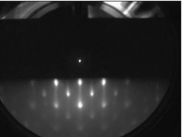
Figure 2.7: RHEED pattern of a MgO (100) single crystal: a) direct beam, b) shadow edge, c) specular (00) beam, d) o ff -specular (02) rod, e) Kikuchi lines
In the ideal case of a perfectly flat crystal and no divergence of the electron beam, the RHEED pattern would consist of spots on a circle. In a real experiment, however, beam divergence and crystal steps can cause some spread in k
0, and thus the radius of the Ewald’s sphere. As the di ff raction condition is less strict in the out-of-plane direction, the spots can elongate in this direction to form streaks. Fig- ure 2.7 shows typical RHEED pattern from MgO (100) single crystal. There are three clearly visible di ff raction spots; the specular (00), 02 and 0¯2 di ff raction lines (rods). The inelastic scattering and multiple scattering e ff ects are also visible in this pattern due to strong intersection between electrons and matter. Kikuchi lines are one of the features that arise from the multiple scattering.
In an island growth, the transmission of the electron beam through the growing
islands still can happen. As the di ff raction geometry is di ff erent in this case, the
pattern changes into spotty. Figure 2.8 shows a typical 3D transmission pattern of
Fe
3O
4islands on SrTiO
3(100) substrate. Depending on the size and the spacing
of the islands, several intermediate cases between a pure reflection pattern and a
Figure 2.8: RHEED pattern of an island growth Fe
3O
4film on SrTiO
3(100) sub- strate.
pure transmission pattern can occur. Each case has completely di ff erent condition.
Therefore, it is possible to distinguish reflection and transmission contributions by rotating the azimuth of the sample. Reflection spots will move, whereas transmis- sion spots will stay.
2.2.2 LEED
Figure 2.9: Schematic view of the LEED set-up [44].
LEED is an in-situ di ff raction technique for structure identification purposes.
In a typical LEED experiment, electrons with kinetic energies between 50 eV and
300 eV impinges perpendicularly on a surface of single crystal having a well or-
dered surface. The electrons are di ff racted by the surface atoms and imaged on a fluorescent screen. The fluorescent screen is situated around the electron gun with a hemispherical shape centered on the crystal surface. A typical construc- tion of LEED set-up is depicted in figure 2.9. In a LEED experiment, the Ewald sphere intersects the lattice rods at particular points that fulfill the Laue condition which defines the scattered wave vectors for di ff racted beams, as shown in fig- ure 2.10. Generally, the normal geometry is less sensitive to the topmost atomic layers. Due to the very short elastic mean free path of the LEED electrons, which range between 5Å and 10Å [45], LEED becomes a highly surface sensitive electron di ff raction technique.
Figure 2.10: The Ewald sphere construction in LEED technique [44].
Figure 2.11 shows typical LEED picture from a well ordered surface of MgO (100) single cystal. The arrangement and the distance of the spots contain infor- mation about the surface lattice symmetry, and the in-plane lattice constant. The sharpness, brightness and profile of the spots denote the quality of the crystallinity.
Intense and sharp spots and low background intensity suggest a well ordered sur- face. On the other hand, broadening and weakening spots, and also an increase background intensity show a presence of structural defects, crystallographic imper- fections and domains. Moreover, the absence of any spots indicates considerably disorder or even polycrystallinity of the surface.
The di ff erence between RHEED and LEED techniques is the radius of the
Ewald sphere. The low electron energy at 150 eV, for example, the electrons wave
length is 1 Å, and the radius of the Ewald sphere is 6 Å
−1, which is only three times
larger than the separation between the reciprocal rods of, for example, MgO (2.1
Figure 2.11: An example of LEED picture for a good crystallinity surface from a MgO (100) single crystal.
Å
−1). Therefore, the Ewald sphere in LEED is comparable to the spacing of the re- ciprocal lattice rods. As a consequence, the intersections of the Ewald sphere with reciprocal lattice rods in LEED are much more sharply defined and the di ff raction features are more similar to spots than to streaks.
Another important di ff erences between RHEED and LEED arise from the ex- perimental geometries. In RHEED, at very grazing incidence and at high kinetic energies (large Ewald sphere radius) only a few Laue zones are practically imaged on the screen which lies parallel to the elongated direction of the reciprocal lattice rods. Therefore, a RHEED pattern is only a projection of a small part of the surface reciprocal lattice. On the other hand, a LEED technique has the plane of the screen perpendicular to the reciprocal lattice rods and the small Ewald sphere radius, so that it can provide a projection of the full surface Bruilloin zone. As a result, the LEED pattern can acquire the full symmetry of an ordered surface, whereas in RHEED it can be attained only by recording pattern at di ff erent azimuthal angles.
In conclusion, RHEED and LEED techniques are two complementary techniques which combination is a powerful tool to study the translational symmetry of surface and interfaces, and the growth mode of thin films.
2.3 X-Ray Di ff raction
X-Ray Di ff raction (XRD) is a technique for structural characterization that can be
done ex-situ. This technique investigates the structure and gives direct information
about the reciprocal space. It can obtain information about the large range order
in the sample. By this technique, the incident X-Ray beam is specularly reflected
from a family of lattice planes at the Bragg angle. Then the scattered beam will
have a sharp maximum intensity. By knowing the scattering angle, the inter planar
distance can be determined from the Bragg law.
Figure 2.12: The X’pert di ff ractometer, a) sample stage, b) x-ray tube, c) hybrid x- ray mirror, d) di ff racted beam optics, and e) detector. This figure is retrieved from Ref. [42].
The XRD measurement in this thesis used a Philips X’pert di ff ractometer as shown in figure 2.12. It was equipped with a hybrid mirror / monochromator for Cu K α radiation ( λ = 1.54056 Å), a 4-circle ganiometer, and a programmable slit in front of the detector. Figure 2.13 shows typical geometry for XRD measurement.
The x-ray source (incident beam) is fixed and the sample is rotated around θ while the detector is moved by 2 θ . The ψ axis allows for 180
◦rotation and the ϕ axis which is perpendicular to the sample surface enables 360
◦rotation. All rotations are done by the 4-circle ganiometer. Based on this set-up, three di ff erent mea- surement modes can be obtained. They are x-ray reflectivity (XRR), θ -2 θ x-ray di ff raction, and reciprocal space mapping (RSM).
XRR is a tool to determine the thickness of poly-crystalline or single crystalline films, and extracting information about the roughness of the surface and the inter- faces. The incident beam irradiates the film at very low angles (0
◦<θ< 4
◦) with respect to the film plane. The di ff racted beam are collected in the detector at an- gle 2 θ with respect to the incident beam after experiencing multiple reflection and refraction at the di ff erent interfaces in the film. The XRR profile shows interface fringes, the period of which indicates the total thickness of the film. The decay of XRR intensity is related to the roughness of the film surface, and of the interface with the substrate.
The θ -2 θ x-ray di ff raction provides information about the chemical phases present
in the sample and the out-of-plane lattice parameter (c). The di ff raction pattern is
obtained in the Bragg-Brentano geometry, where the incident beam is directed to
the sample at an angle θ with respect to the surface plane. Then, the intensity of the
reflected beam is measured at an angle 2 θ with respect to the incident beam. Due to
Figure 2.13: Schematic drawing of XRD geometry. This figure is retrieved from Ref. [46].
this specific geometry, the incident beam is scattered at a certain Bragg angle only at the lattice planes hkl, which are parallel to the sample surface. The out-of-plane lattice parameter can be evaluated using the Bragg equation:
2d
hklsin θ = n λ (2.3)
where n is an integer and has a meaning of the reflection order, λ is the wave- length, θ is the di ff raction angle and d
hklis the interplanar spacing and in case of cubic crystal equal to :
d
hklsin θ = c
√ h
2+ k
2+ l
2(2.4)
The RSM measurement is used to study the in-plane quality of the grown film to the substrate. It can obtain information about the in-plane lattice parameter (a), the growth mode, the relaxation state, and even the imperfections in strained. This measurement is acquired by performing a set of θ -2 θ versus ω scans at di ff erent ω angles around a non-specular reflection common to the film and the substrate. The 2 θ and ω are the detector and sample orientations with respect to the direction of the incident beam.
2.4 Spectroscopy
When atoms condense into solids, the electronic states of the outer electron, which
is named the valence electron states (VES), are strongly a ff ected depending on the
atomic species and their arrangements in solids. The characteristic features of VES
will influence the properties of the solids. The VES comprise the partially filled conduction band states in metals and the filled valence and empty conduction band states in insulator, including the 3d electrons states of transition metal (TM) ele- ments. Therefore, the study of VES is important in solid state physics. On the other side, inner electron (core electrons) of atoms are deeply bound inside the atoms and unchanged even when the atoms condense into solids. Core level spectroscopy is a powerful tool to study the characteristic of solid. It will excite a core electron by incident x-rays. In order to excite the core electrons, the incident x-rays must have energies larger than the core level binding energies. Every photon being ab- sorbed by a solid must have created some kind of excitation, and by studying the intensities related to these excitations many properties of the solid can be revealed.
a) XPS process
b) XAS process
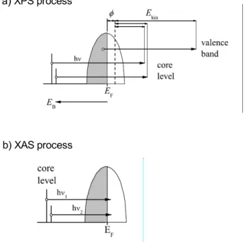
Figure 2.14: Schematic representation of XPS and XAS excitation process by using the independent particle picture. Taken from Ref. [47]
There are various kinds of core level spectroscopy, two of the famous ones
are X-ray Photoelectron Spectroscopy (XPS) and X-ray Absorption Spectroscopy
(XAS). They are also used in this thesis to provide information about electronic
properties of Fe
3−xCo
xO
4thin films. Figure 2.14 shows schematically the process
for a simple case of these spectroscopy. In the case of XPS, a core electron is
excited by the incident x-ray to the high-energy continuum states and detected as
a photoelectron. On the other hand, in the XAS, a core electron is excited near
to the excitation threshold just above the Fermi level. Therefore, the XPS reveals
information on the occupied electronic states, while XAS probes the unoccupied states.
2.4.1 XPS
XPS is a powerful technique to study the surface physics that can provide valu- able information about the electronic structure and the chemical composition of the film. It works based on the photoelectric e ff ect, which is the emission of elec- trons from a material caused by incoming photons. The energy conservation law in the photoemission process is the basis for the photoelectron spectroscopy:
E
kin= h ν − E
B− ϕ, (2.5)
where E
kinis the kinetic energy, h ν the energy of the incoming x-rays, E
Bde- notes the binding energy, and ϕ the work function of electron analyzer. By analyz- ing the E
kinfrom the emission electron, the E
Bof the electron in the material can be deduced.
The XPS spectrum is commonly constructed by sharp peaks at the binding en- ergies corresponding to the core levels of the elements in the sample which come from photoelectrons with negligible energy loss. A background feature in the XPS spectrum comes from photoelectrons su ff ering energy losses due to inelastic scat- tering with others electrons inside the solid. A small deviation of E
Bfrom the free atom value, which is denoted by the chemical shift, provides information on the chemical bonding of VES. Auger electrons peaks are also usually seen in the XPS spectrum. Auger electrons are emitted with the kinetic energies that are gained via the decay process of an electron from a higher energy level into the core hole that was created by the incoming x-rays. The kinetic energy of the Auger peaks is in- dependent to the energy of the x-ray source. Besides studying the XPS core levels line shape, it is also great interest to study the valence band spectra. It contains a lot of information on the electronic properties of the sample.
In a one-electron approximation, the XPS spectrum can be explained with the
occupied density of electronic states. If the system is weakly correlated, this ap-
proximation may be valid and methods like e.g. density-functional theory can be
used to describe the spectrum of the valence band. Therefore, another method is
needed to address for a correlated electrons system. There are two simple bases
for understanding the photoemission process [48–50]. As a three-step process, it
is divided into the excitation of the photoelectron, the traveling to the surface, and
the escape from the solid into the vacuum. The photoemission process can also
be considered as a one-step process, where a many body state with n electrons (as
the ground state) is transformed into a final state with n − 1 electrons plus a free
photoelectron. The biding energy is therefore defined as the di ff erence between the
total energies of the excited final state and the ground state. A formulation of the one-step process is to express the spectral function of the photoemission as the one- particle Green’s function [51]. Full-multiplet calculations like described in some literatures can also be used to interpret XPS spectra [47, 48, 52].
The many-body charge-transfer e ff ect in the XPS spectrum can be observed as an asymmetry of the spectral shape and as satellite structures. It can be explained when the core hole is created in the XPS process, VES are polarized by the core hole potential and screen it. The polarization of VES occurs mainly by the charge transfer e ff ect. Thus, the core hole plays a role of ’test charge’, which induces the charge transfer of VES, and the e ff ect of charge transfer is reflected in the XPS spectrum.
Figure 2.15: A typical XPS set-up. Taken from Ref. [53]
Typical XPS experiment consists of photon source (x-ray source), sample, an-
alyzer and detector as shown in figure 2.15. The x-ray source is constructed by
an electron gun, a water-cooled Al anode, and a Vacuum Generators twin crystal
monochromator. An electron gun generated electrons and then accelerated up to
10 kV and focused on the water-cooled Al anode. After that it will emit a char-
acteristic x-ray spectral lines together with a continuous background. The x-ray
will be monochromatized by Bragg refraction at two separately adjustable quartz
crystal for the Al K α radiation at 1486.6 eV. The monochromatized x-ray is finally
focused onto the sample. The photoemission electrons are emitted from the sample
and then collected using the Grammadata Scienta R3000 electron energy analyzer
unit. It consists of an electron lens system, a hemispherical deflection analyzer, and
a micro-channel plate (MCP) with phosphor screen as a detector unit. The electron
lens system will focus the photoelectrons onto the analyzer entrance slit, and then
decelerate (or accelerate) their kinetics energies in order to be matched with a se-
lected energy scanning range. At the hemispherical analyzer, an electrostatic filed within two concentric hemispheres with radii of 110 mm and 190 mm is estab- lished to only allow photoelectrons of a given energy (the so-called pass energy) to arrive at the detector slits and onto the MCP detector itself. The MCP works as an electron multiplier with a gain of the order of 10
6. These electrons will arrive at the phosphor screen, where light flashes are emitted and subsequently recorded by a CCD camera. The position of the light flash is then related to the kinetic energy of the photoelectron. The detection unit is connected to a computer and controlled via the SES software.
2.4.2 XAS
XAS is a spectroscopy technique where a core electron is exited near to the thresh- old by the incident x-ray through the electric dipole transition. Since the core electron state is known, the XAS spectrum delivers information on the symmetry- projected partial density of state of the exited states. The projected symmetry de- pends on the symmetry of the core-electron states and the selection rule of the photo-excitation including the polarization of the incident x-ray.
In XAS technique, it measures the photon energy dependent absorption of x-ray in a sample. The absorption of x-ray can be measured by using yield mode. Here, secondary e ff ects are used to measure the absorption cross section. Upon relax- ation from the photo-excited state, fluorescence photons, Auger electrons, photo- electrons, and even ions are emitted from the sample. They are supposed to give a signal that is proportional to the absorption cross section [54]. The detection tech- nique which is used in this thesis is so-called total electron yield (TEY). It is the most frequently used detection mode because of its convenience to be implemented by collecting the drain current. The drain current is the net current of all charged particles emitted from the sample so that it can measure with high accuracy. The TEY has a probing depth about 40 Å which is good enough to measure thin film sample [55].
The interaction of x-ray with the matter can be described by Fermi’s golden rule. Whereas, the probability W of a system for a transition between initial state ψ
iand final state ψ
fcan be describe as the following [48]:
W = 2 π
~ |⟨Ψ
f| T |Ψ
i⟩|
2δ (E
f− E
i− ~ω ) , (2.6) E
iand E
fare described as the total energies of the initial and final state. T is the transition operator. It is defined by dipole approximation which is customary written as:
T = e ˆ
q· r , (2.7)
The dipole operator is only non-zero if the orbital quantum number of final and initial state di ff er by 1, and the spin is conserved, thus, ∆ L = ± 1 and ∆ S = 0.
Due to dipole selection rules, XAS is quite selective in multiplet structures.
It determines the final states that can be reached and with what intensity, starting from a certain initial state. As a consequence, only limited access can be visible as separate structures in the spectrum. Therefore, XAS is extremely sensitive to the symmetry of the initial state, i.e., the spin, orbital, and valence states of the element.
670 680 690 700 710 720 730 740 750 760 770 780 continuum
edge jump L
2 fine
structure L
3 fine
structure
20 nm Fe 3
O 4
// MgO
Intensity (a.u)
Photon Energy (eV) photo-
absorption
back ground
![Figure 2.5: Schematic drawing of the MBE set-up. This figure is retrieved from [42].](https://thumb-eu.123doks.com/thumbv2/1library_info/3699159.1505939/17.892.269.636.438.721/figure-schematic-drawing-mbe-set-figure-retrieved.webp)
![Figure 2.15: A typical XPS set-up. Taken from Ref. [53]](https://thumb-eu.123doks.com/thumbv2/1library_info/3699159.1505939/28.892.242.629.452.687/figure-a-typical-xps-set-taken-from-ref.webp)


