Research Collection
Doctoral Thesis
Lead-Free Low-Dimensional Main Group Metal Halides: New Self-Trapped Excitonic Emitters and Their Applications
Author(s):
Benin, Bogdan M.
Publication Date:
2020-08
Permanent Link:
https://doi.org/10.3929/ethz-b-000446190
Rights / License:
In Copyright - Non-Commercial Use Permitted
This page was generated automatically upon download from the ETH Zurich Research Collection. For more information please consult the Terms of use.
ETH Library
DISS. ETH NO. 27018
LEAD-FREE LOW-DIMENSIONAL MAIN GROUP METAL HALIDES: NEW SELF- TRAPPED EXCITONIC EMITTERS AND THEIR APPLICATIONS
A thesis submitted to attain the degree of DOCTOR OF SCIENCES of ETH ZURICH
(Dr. sc. ETH Zurich)
presented by Bogdan Markovich Benin
Master of Science Kent State University
Born on 05.04.1993
citizen of the United States of America
Accepted on the recommendation of Prof. Dr. Maksym V. Kovalenko, examiner Prof. Dr. Markus Niederberger, co-examiner
2020
Declaration
I hereby confirm that I am the sole author of the written work herein enclosed and that I have compiled it in my own words. Parts excepted are corrections of form and content by the supervisor.
Title of work:
Lead-Free Low-Dimensional Main Group Metal Halides: New Self-Trapped Excitonic Emitters and Their Applications
With my signature I confirm:
− I have committed none of the forms of plagiarism.
− I have documented all methods, data, and processes truthfully.
− I have not manipulated any data.
− I have mentioned all persons who were significant contributors to this work, as described below.
− I obtained copyright permissions from the journal for reproducing the text and Figures in this thesis, where needed.
− I am aware that the work may be screened electronically for plagiarism.
Place, date Signature(s)
Winterthur 20.07.20
Dr. S. Yakunin (ETH Zürich) performed numerous optical experiments including both RT and temperature dependent PL, PLE, and TRPL as well as quantum yield determination for Chapters 2-5. He also did much of the data processing and analysis for thermal imaging as well as the thermometric precision experiments in Chapter 3.
Dr. K.M. McCall (ETH Zürich) assisted with much of the crystallography in Chapter 4 and 5. He also performed the Raman measurements and some of the temperature dependence measurements in Chapter 4.
Dr. M. Wörle (ETH Zürich) assisted and checked all the crystallography throughout this dissertation. He also performed the single crystal measurements in Chapter 2.
Dr. D.N. Dirin (ETH Zürich) assisted in the characterization and description of the materials in Chapter 2.
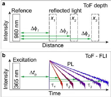
Dr. S. Cattaneo and Dr. C. Hofer (CSEM) developed the ToF-FLI imager used in Chapter 3.
Dr. Y. Shynkarenko (ETH Zürich) played a significant role in the data treatment and analysis for thermal imaging in Chapter 3. He also performed several optical experiments including quantum yield and absorption coefficient determination (Chapter 4 and 5).
Dr. G. Raino (ETH Zürich) performed he temperature dependent PL measurements in Chapter 2.
Dr. O. Nazarenko (ETH Zürich) assisted with the solid-state growth of materials in Chapter 2. She additionally prepared one of the materials utilized in Chapter 3.
Dr. M.I. Bodnarchuk (ETH Zürich) prepared one of the materials utilized in Chapter 3.
M. Aebli (ETH Zürich) performed the ssNMR experiments and processed all the relevant data in Chapter 4.
Dr. F. Krumeich (ETH Zürich) took SEM images and performed EDS measurements in Chapter 2.
V. Morad (ETH Zürich) performed the DFT calculations in Chapter 2 and 4.
K. Sakhatskyi (ETH Zürich) performed electrical characterization as well as photoconductivity and X-ray photoconductivity measurements of the materials presented in Chapters 4 and 5.
M. Fischer (ETH Zürich) prepared some of the polycrystalline powders of materials presented in Chapter 2.
D. Borgeaud dit Advocat (ETH Zürich) prepared some of the single crystals of materials presented in Chapter 5.
Acknowledgements
There is an African proverb, “it takes a village to raise a child.” Well, it takes a research group to raise a researcher.
First, I want to thank the head of that research group, Prof. Dr. Maksym V. Kovalenko for the opportunity to come to his group, to find my niche, for supporting my work, and offering his guidance.
I want to thank Prof. Dr. Markus Niederberger for accepting to evaluate my dissertation and act as a co-referee for the final examination.
This dissertation would not have been possible without the numerous contributions, support, and mentorship of Dr. Sergii Yakunin, Dr. Michael Wörle, Dr. Dmitry N. Dirin, and Dr. Kyle M.
McCall. At the same time, I want to thank Dr. Yevhen Shynkarenko, Viktoriia Morad, and Marcel Aebli for providing optical measurements, calculations, and NMR measurements.
Furthermore, the entire Kovalenko group has been an amazing team of researchers and colleagues to work with, and I look forward to seeing what each person achieves in the coming years.
Additionally, I will always fondly remember the open and creative environment (and the never- ending supply of sweets) fostered by Kyle and Martin in H111.
I want to specially thank Marcel, Dominic, Matthias, Matyas, Dylan, Nick, Laura, Marco, Kyle, Sergii, Federico, Michael, Darius, Matt, Ryan and a few others for, at one point or another, sharing a bite or a drink and stirring-up new ideas or just lightening the mood.
Finally, I thank my parents, Mark & Galina Benin, and Aylin Crugnale, for their inexhaustible support and love.
Table of Contents
Declaration... ii
Acknowledgements ... iv
Table of Contents ... v
List of Abbreviations ... viii
Abstract ... x
Zusammenfassung... xii
Chapter 1. Metal-halides and their dimensional diversity ... 1
1.1. A brief history of luminescent materials ... 1
1.2. Lead-halide perovskites ... 3
1.3. Lead-free alternatives... 5
1.3.1. AMX3 alternatives ... 6
1.3.2. Double perovskites — In+, Sb3+, and Bi3+ ... 6
1.4. Lowering dimensionality ... 8
1.4.1. General trends ... 8
1.4.2. Self-trapped excitons ... 9
1.4.2.1. Excitons...9
1.4.2.2. Wannier-Mott and Frenkel excitons ...10
1.4.2.3. The Importance of phonons and polarons ...11
1.4.2.4. Self-trapped excitons ...11
1.4.3. Two-dimensional metal-halides ... 12
1.4.4. One-dimensional materials ... 14
1.4.5. Zero-dimensional materials ... 16
1.4.5.1. Overview ...16
1.4.5.2. Applications for 0D metal-halides ...20
1.5. Thesis outline ... 22
Chapter 2. Highly Emissive Self-Trapped Excitons in Fully Inorganic Zero-Dimensional Tin Halides ... 25
2.1. Abstract ... 25
2.2. Introduction ... 27
2.3. Experimental details... 27
2.4. Results and Discussion ... 28
2.5. Conclusion ... 36
Chapter 3. High-resolution remote thermometry and thermography using luminescent low- dimensional tin-halide perovskites ... 37
3.1. Abstract ... 37
3.2. Introduction ... 38
3.3. Experimental details... 40
3.4. Results and Discussion ... 40
3.5. Conclusion ... 52
Chapter 4. The Rb7Bi3-3xSb3xCl16 family: A Fully Inorganic Solid Solution with Room- Temperature Luminescent Members ... 53
4.1. Abstract ... 53
4.2. Introduction ... 54
4.3. Experimental details... 55
4.4. Results and Discussion ... 55
4.5. Conclusion ... 81
Chapter 5. Intervalent and mixed-valent zero-dimensional metal-halides of the Rb23SbIII7- xBiIIIxSbV2Cl54 family (x≤3.5)... 82
5.1. Abstract ... 82
5.2. Introduction ... 83
5.3. Experimental Methods ... 85
5.4. Results and Discussion ... 85
5.5. Conclusion ... 96
Chapter 6. Summary and Outlook ... 98
6.1. Summary ... 98
6.2. Outlook ... 98
6.2.1. Luminescent solar concentrators ... 100
6.2.2. Fluorescent-lifetime encoded security tags ... 101
6.2.3. “STED” microscopy and FLIM-nanoscopy ... 101
Chapter 7. Materials and Methods... 104
7.1. Materials ... 104
7.2. Synthetic procedures ... 104
7.2.1. Cs4SnBr6 synthesis ... 104
7.2.2. Cs4-xAxSn(Br1-yIy)6 (A = Rb, K; x ≤ 1, y ≤ 1) synthesis ... 105
7.2.3. Rb7Sb3Cl16 synthesis ... 105
7.2.4. K7Sb3Cl16 synthesis ... 105
7.2.5. Rb7Bi3Cl16 synthesis ... 105
7.2.6. Rb7Bi3-3xSb3xCl16 synthesis ... 106
7.2.7. Rb23BiIII7-xSbIIIxSbV2Cl54 synthesis ... 106
7.3. Structural Characterization ... 107
7.3.1. Powder X-ray Diffraction... 107
7.3.2. Single-Crystal X-ray Diffraction ... 107
7.3.3. Scanning Electron Microscopy and Energy-Dispersive X-ray Spectroscopy 107 7.3.4. 87Rb NMR ... 107
7.4. Optical characterization ... 108
7.4.1. UV-Vis Diffuse Reflectance Measurements ... 108
7.4.2. RT PL and PLE Measurements ... 108
7.4.3. Absolute PLQY measurements ... 108
7.4.4. RT TRPL ... 108
7.4.5. Absorption Coefficient determination ... 108
7.4.6. dT-PL, dT-PLE, dT-TRPL, TRES, dW-PL Measurements ... 109
7.4.6.1. Cs4-xAxSn(Br1-yIy)6 (A = Rb, K; x ≤ 1, y ≤ 1) ...109
7.4.6.2. Rb7 Bi3-3xSb3xCl16 and K7Sb3Cl16 ...109
7.4.7. Raman... 109
7.4.8. DFT calculations ... 110
7.4.8.1. Cs4-xAxSn(Br1-yIy)6 (A = Rb, K; x ≤ 1, y ≤ 1) ...110
7.4.8.2. Rb7 Bi3-3xSb3xCl16 and K7Sb3Cl16 ...110
7.4.9. Conductivity and X-ray photoconductivity measurements ... 111
Chapter 8. Appendix ... 112
8.1. Appendix to Chapter 2 ... 112
8.2. Appendix to Chapter 3 ... 133
8.3. Appendix to Chapter 4 ... 143
8.4. Appendix to Chapter 5 ... 183
References ... 198
Curriculum Vitae ... 223
List of Abbreviations
CB Conduction Band
CC Configurational Coordinate CRI Color Rendering Index DFT Density Functional Theory DOS Density of States
dT-PL Temperature dependent Photoluminescence
dT-PLE Temperature dependent Photoluminescence Excitation dT-TRPL Temperature dependent Time-Resolved Photoluminescence dW-PL Power dependent Photoluminescence
EDS Energy Dispersive X-ray Spectroscopy
FA Formamidinium
FLI Fluorescence Lifetime Imaging
FLIM Fluorescence Lifetime Imaging Microscopy FOM Figure-Of-Merit
FWHM Full-Width-at-Half-Maximum HOMO Highest Occupied Molecular Orbital
ICP-MS Inductively Coupled Plasma Mass Spectrometry IR Infrared
KM Kubelka-Munk
LED Light Emitting Diode
LSC Luminescent Solar Concentrator LUMO Lowest Unoccupied Molecular Orbital
MA Methylammonium
MQMAS Multi-Quantum-Magic-Angle Spinning NC Nanocrystal
PCE Power Conversion Efficiency PL Photoluminescence Spectroscopy
PLE Photoluminescence Excitation Spectroscopy PXRD Powder X-Ray Diffraction
QY/PLQY Photoluminescence Quantum Yield ROT Remote-Optical Thermography RT Room-temperature
SCXRD Single Crystal X-ray Diffraction SEM Scanning Electron Microscopy SHG Second Harmonic Generation SSL Solid-State Lighting
ssNMR Solid-State Nuclear Magnetic Resonance
STCTE Self-Trapped Charge-Transfer Exciton STE Self-Trapped Exciton
STED Stimulated Emission Depletion
TCSPC Time-Correlated Single Photon Counting ToF Time-of-Flight
TRES Time-Resolved Emission Spectroscopy TRPL Time-Resolved Photoluminescence UV-Vis Ultraviolet-Visible
VB Valence Band XRD X-Ray Diffraction
µ Mobility-Lifetime Product 0D Zero-Dimensional
1D One-Dimensional 2D Two-Dimensional 3D Three-Dimensional
Abstract
LEAD-FREE LOW-DIMENSIONAL MAIN GROUP METAL HALIDES: NEW SELF- TRAPPED EXCITONIC EMITTERS AND THEIR APPLICATIONS
Bogdan Markovich Benin
Metal-halide based semiconductors have been in the limelight for the past few years as a result of the outstanding performance of devices in a variety of optoelectronic applications utilizing lead-halide perovskites. Lead-free materials based on Sb, Sn, or Bi with a three-dimensional (3D) framework, on the other hand, have yet to provide a true alternative.
This thesis instead explores the field of low-dimensional, specifically zero-dimensional (0D), lead-free metal-halides as luminescent materials. These 0D materials contain disconnected metal-halide octahedra, which drastically alters their optoelectronic properties compared to fully connected 3D structures and, prior to 2017, the library of such 0D metal-halides was exceedingly small.
This work began with the study of the optical properties of one known yet uninvestigated incongruently melting phase — Cs4SnBr6. This material was found to exhibit broad yet efficient room temperature photoluminescence (RT PL), which occurs as a result of the recombination of self-trapped excitons (STEs). The STE emission in this phase was then found to be compositionally tunable within the Cs4-xAxSn(Br1-yIy)6 (A=Rb,K; x,y≤1) family. The discovery of this and other phases by the community prompted a closer look at the optical properties of various additional Sn- based 0D and 1D materials such as (C4H14N2I)4SnI6 and [C(CH2)3]2SnBr4. In doing so, it became evident that their PL lifetimes were extremely temperature dependent (~ 20 ns/K). This opened the door to using 0D metal-halides as remote-optical thermometric and thermographic luminophores i.e. materials which can be used to optically determine temperature. In addition to this thermal sensitivity, this emission process was found to be intrinsic and incredibly robust with no changes to the PL lifetime observed between synthetic batches or after partial degradation or partial oxidation. These two factors together allowed for a thermometric precision of ±13 mK.
Although this was quite impressive, the fact of the matter remained that these are still tin- based materials and they will, inevitably, fully oxidize. This inspired the dimensional reduction of the pnictogen halides to discover new, oxidatively stable 0D materials for remote-optical thermometry. This resulted in the Rb7Bi3-3xSb3xCl16 (x≤1) family of materials, which also exhibit STE PL with a similar thermal sensitivity as the tin-based materials. Furthermore, these structures contain edge-shared octahedral dimers, which were determined to be the source of RT PL and the luminescent properties of structures containing them have not been previously investigated.
This work also led to the discovery of a new set of mixed-valent materials with the composition Rb23MIII7SbV2Cl54 (MIII = Bi, Sb). These 0D structures contain octahedra of with
various oxidation states (3+ and 5+) and exhibit intense colors as a result of intervalent/mixed- valent charge transfer. While non-luminescent even at 12 K, these materials do exhibit relatively high mobility-lifetime products under X-ray illumination, suggesting that the site-to-site tunneling through this structure may provide a potentially useful tool for new X-ray and hard-radiation detector materials.
In summary, the work presented here has resulted in several, substantial contributions to the low-dimensional metal-halide community, which include the synthesis and characterization of several new materials as well as the identification and successful demonstration of remote-optical thermometry/thermography as a new application for this class of materials. This dissertation serves as an effective foundation for further research in the field by giving other researchers an overview of the field as well as insights into potentially interesting avenues for investigation, both for materials as well as possible applications.
Zusammenfassung
LEAD-FREE LOW-DIMENSIONAL MAIN GROUP METAL HALIDES: NEW SELF- TRAPPED EXCITONIC EMITTERS AND THEIR APPLICATIONS
Bogdan Markovich Benin
Metallhalogenid basierende Halbleiter standen in den letzten Jahren durch die herausragende Leistung von Elementen für optoelektronische Anwendungen, unter Verwendung von Bleihalogenid Perowskiten, im Rampenlicht. Im Gegensatz dazu müssen sich bleifreie Materialien, welche sich auf einem dreidimensionalen (3D) Netzwerk mit Sb, Sn oder Bi basieren, erst noch als nützliche Alternative beweisen.
Diese Doktorarbeit erkundet das Feld der niedrigdimensionalen, insbesondere die nulldimensional (0D), bleifreien Metallhalogeniden als lumineszente Materialien. Diese 0D Materialien bestehen aus abgetrennten Metallhalogenid-Oktaeder, was die optoelektronischen Eigenschaften drastisch verändert im Vergleich zu den vollkommen verknüpften 3D Strukturen.
Vor dem Jahr 2017 war die Sammlung solcher 0D Metallhalogeniden äusserst klein.
Diese Arbeit begann mit der Studie der optischen Eigenschaften einer bereits bekannten, aber noch nicht untersuchten inkongruent schmelzender Phase – Cs4SnBr6. Dieses Material zeigt eine breite, aber effiziente Photolumineszenz bei Raumtemperatur (RT PL), welche durch die Rekombination von selbstfangende Exzitonen (STEs) hervorgerufen wird. Die STE-Emission in dieser Phase kann durch Veränderung der Komposition innerhalb der Cs4-xAxSn(Br1-yIy)6
(A=Rb,K; x,y≤1) Familie eingestellt werden. Die Entdeckung dieser und anderer Phasen von der Gemeinschaft regte zur Untersuchung der optischen Eigenschaften von zahlreichen Sn- basierenden 0D und 1D Materialien wie (C4H14N2I)4SnI6 und [C(CH2)3]2SnBr4 an. Dabei wurde ersichtlich, dass deren PL Lebensdauer extrem temperaturabhängig sind (~ 20 ns/K). Dies öffnete die Tür um 0D Metallhalogenide als fern-optisch thermometrisch und thermographische Luminophore zu verwenden. Zusätzlich zu dieser Temperaturempfindlichkeit ist die Emission intrinsisch und unglaublich robust. Kein Unterschied in der PL Lebensdauer kann im Vergleich von mehreren Synthesen, teilweiser Zersetzung oder Oxidation beobachtet werden. Diese zwei Faktoren zusammen erlauben eine thermometrische Präzision von ±13 mK.
Dies ist zwar sehr beeindruckend, jedoch bleibt die Tatsache bestehen, dass diese Zinn basierende Materialien unvermeidlich komplett oxidieren.
Daher stammte die Inspiration zur Entwicklung neuer niedrigdimensionaler Pnictogenhalogeniden. Diese nulldimensionalen Strukturen sind stabil gegenüber Oxidation und geeignet für fern-optische Thermometrie. Die Rb7Bi3-3xSb3xCl16 (x≤1) Familie, welche ebenfalls STE PL mit einer vergleichbaren thermischen Empfindlichkeit wie die Zinn basierten Materialien zeigen, waren das Resultat dieser Untersuchung. Des Weiteren beinhalten diese Strukturen
kantenverknüpfte Oktaeder Dimere, welche als Quelle der RT PL ermittelt wurden. Die lumineszenten Eigenschaften von Strukturen mit diesem Merkmal wurden bisher noch nicht untersucht.
Diese Arbeit führte auch zur Entdeckung von einem neuen Set aus Materialien der Komposition Rb23MIII7SbV2Cl54 (MIII = Bi, Sb), welche gemischte Oxidationszustände gleichzeitig beinhalten. Diese 0D Strukturen bestehen aus Oktaedern mit den nominellen Oxidationszuständen 3+ und 5+ und zeigen eine intensive Färbung auf Grund des Ladungstransfers zwischen den verschiedenen Zuständen. Obwohl sie selbst bei 12 K keine Lumineszenz zeigen, besitzen sie dennoch hohe Mobilitäts-Lebenszeiten Produkte unter Röntgenstrahlung, was auf einen Tunnelvorgang von einer Stelle zu einer anderen hindeutet. Dies macht diese Verbindungen zu möglichen Detektormaterialien für Röntgen- und weiterer Hochenergiestrahlung.
Zusammenfassend zeigt die hier präsentierte Arbeit zahlreiche, wesentliche Beiträge für die niedrigdimensionierten Metallhalogenid-Gemeinschaft, welche die Synthese und die Charakterisierung von mehreren neuen Materialen, sowie die Identifikation und erfolgreichen Demonstration von fern-optischer Thermometrie/Thermographie als neue Anwendung für diese Klasse an Materialien beinhaltet. Diese Doktorarbeit dient als effektives Fundament für weitere Forschung in diesem Feld, indem es eine breite Übersicht, sowie genauere Einblicke in die Untersuchung und Entwicklung von Materialien und möglichen Anwendungen gewährt.
Chapter 1. Metal-halides and their dimensional diversity
1.1. A brief history of luminescent materials
The tendency for some materials to “glow-in-the-dark” or phosphoresce, or for other materials to exhibit colors only under certain conditions (fluorescence) has been observed, although not understood, since at least the renaissance.1 At this time, several doctors and scholars took note of various wood-bark samples, which were collected from the then “new world” of Mexico, that would result in a blue aqueous solution after soaking the wood. These same bark samples would later be studied by 17th century scientists in an effort to understand the origin of this color.2-5
Figure 1.1. An image of an alkaline aqueous solution containing Eysenhardtia polystachia under daylight illumination. Reprinted (adapted) with permission from J. Chem. Educ. 2011, 88, 6, 731-738.
Copyright 2011 American Chemical Society.
Newton even describes such a solution in his treatise on optics.6 In the end, he concluded that the blue color is a sort of reflection rather than the emission that we understand today.
By the 19th century, several additional luminescent solutions and materials were identified such as “Bolognian phosphor” or a doped barium sulfide;5 fluorospar — now referred to as fluorite or CaF2;7-8 an alcoholic infusion of leaves (chlorophyll);9 and quinine (a bitter antimalarial molecule that was made more palatable with the invention of tonic water).5, 10-12
It was not until 1852, however, that the term fluorescence, utilized eponymously after fluorite, was attributed to the ability of certain materials to “… cause the sensation of light” by Sir George Stokes.13-14 The experiment that Stokes used to identify this property as something other than reflection was by splitting sunlight into its components with a prism and then passing a quinine solution through each component until he observed that the colorless area after violet (ultraviolet) resulted in the test tube to glow blue. Around the same time, a French scientist,
Edmond Becquerel, performed a similar experiment on calcium sulfide and discovered what he would later term phosphorescence.5, 15-16 Later in 1888, the general term luminescence was introduced as an umbrella term for the emission of light from a material.17 Since then this phenomenon has been observed in a wide variety of materials such as organic molecules and dyes, proteins, inorganic salts, transition metal and rare-earth doped materials, diamonds, and semiconductors. In fact, the luminescent fluorite that Stokes and others studied has since been identified as Eu2+-doped CaF2.18
Figure 1.2. A sample of blue-luminescent fluorite from the U.K. Photo by Didier Descouens - Own work, CC BY-SA 4.0; https://commons.wikimedia.org/w/index.php?curid=7528654)
While these have all found use in some application, some of the most versatile and important materials are semiconductors, which have been used in a plethora of applications in the modern age: scintillation, computer displays, lasers, communication, high-speed internet — all thanks to the ability of these solid-state materials to emit light.19 Some of the best-known examples of luminescent semiconductors today include Ga1-xAlxN, GaAs, InP, CdSe, CdTe, PbS, and HgTe;
between these materials the entire range from ultraviolet (UV) to infrared (IR) light up to nearly 4 μm is covered.20-21 The utility of these materials also stems from their ability to be compositionally tuned and made into thin-films and nanocrystals (NCs). For instance, blue light emitting diodes (LEDs) are made with thin films of GaN, and their emission can be redshifted through In-doping. The global adoption of this technology led to the 2014 Nobel prize in physics being awarded to Akasaki, Amano, and Nakamura for “the invention of efficient blue light-emitting diodes which has enabled bright and energy-saving white light sources.”22 Furthermore, materials such as InP, CdSe, CdTe, and PbS have also been demonstrated to be excellent emitters when prepared as quantum dots, and InP quantum dots have even been commercialized by Samsung in their QLEDTM televisions as green and red phosphors.23 As impressive as these materials are as visible phosphors, they all continue to face considerable synthetic and regulatory barriers.
There has been a growing need for materials discovery in the solid-state and materials
chemistry communities to discover brighter and more efficient light sources. One recent success story, which have also inspired our own efforts, are the lead-halide perovskites.
1.2. Lead-halide perovskites
Although the perovskite classification has been known since 1839 with the discovery of CaTiO3, these cubic structures would not enter the limelight until 2012 with the use of MAPbI3
(MA = CH3NH3+) as an absorptive layer in a solar cell.24-27
The general formula for these metal-halide materials is ABX3, in which A is a large, monovalent cation such as Cs+, MA, or CH(NH2)2+ (FA) that sits in the cuboctahedral voids of an anionic framework composed of corer-sharing BX6 octahedra. B is a divalent main group metal such as Pb2+ or Sn2+, and X is Cl-, Br-, or I- (Figure 1.3).
Figure 1.3. Ideal cubic ABX3 perovskite. The large, central A-site cation is a blue sphere, which is typically Cs, MA, or FA in the case of halide perovskites; the surrounding anionic framework is shown as corner-sharing BX6octahedra (grey and red), which are typically composed of Pb or Sn as the B cation and Cl, Br, or I as the X halide. Structure generated using CaTiO3 as a template (ICSD# 16925).
The stability of this cubic structure is dictated by a geometric restraint known as the Goldschmidt tolerance factor:28
𝑡 = (𝑟𝑎+𝑟𝑥)
√2(𝑟𝑏+𝑟𝑥) (1)
in which ra is the radius of the A-site cation, rb is the radius of the B-site cation, and rx is the radius of the halide. An ideal cubic structure is therefore stable when 0.8 ≤ t ≤ 1.0. As this value decreases
below 0.8 the structure distorts to a lower symmetry and adopts a structure with edge shared polyhedra similar to those present in NH4CdCl3.29 This is observed in RbPbI3 and CsPbI3 (although the Cs-analogue is able to also adopt distorted tetragonal structures as well). Values of t ≥ 1 tend to result in structures containing face-shared octahedra with hexagonal symmetry (Figure 1.4).
Figure 1.4. The influence of cation size on the perovskite structure. These structures were generated in Vesta using CCDC-1819569 (FA), ICSD-97851 (Cs, Pbnm), ICSD-161480 (Cs, Pnma), ICSD-194995 (MA), ICSD-6067 (Rb).29-32
While solar cell research has been revolutionized by the utilization of lead-iodide perovskites, lead-bromide and lead-iodide based perovskites have also launched a renaissance in numerous other optoelectronic fields such as LEDs, lasers, scintillation, full-color imaging, photodetection, and X-ray and hard-radiation detection.33-40
The miraculous improvements that these materials bring about to these other fields is attributable to three special characteristics of the metal-halide perovskite structure: softness/ease- of-production, tunability, and defect-tolerance. These materials have been often referred to as
“soft” given their ionic nature and low melting points (CsPbBr3 melts at 567 °C).41 This has opened numerous possibilities for the growth of these materials as single crystals from solution,42-45 the mechanochemical synthesis of NCs,46 or as inclusions in other templates47 or matrices.48-49
Among the most optoelectronically relevant semiconductors (e.g. CdSe, PbS, InP), the optical properties cannot be as easily or rapidly altered as in lead-halide perovskites.50 This is related again to the soft lattice as well as a low defect density and high ionic mobility within these materials.45, 51 As halide vacancies migrate through the structure, new anions from a surrounding growth solution are easily incorporated, leading to fast anion exchange.50 Most importantly, the alteration of the halide composition directly affects the band gap and the photoluminescence (PL)
of these materials as the valence band (VB) comprises Pb 6sand X np orbitals whereas the conduction band (CB) is composed of predominantly Pb 6p orbitals (Figure 1.5).52-54
Figure 1.5. A comparison of the band-edge states in defect-tolerant lead-halide perovskites and traditional defect-intolerant materials such as CdSe or GaAs. From Science, 358 (6364), 745-750.
Reprinted with permission from AAAS. Reprinted (adapted) with permission from Chem. Mater. 2017, 29, 11, 4667–4674. Copyright 2017 American Chemical Society.
This not only results in the facile bandgap variation that has been observed in such materials, but also in the apparent defect-tolerance that these materials possess.47, 49, 53-57 Contrary to traditional semiconductors such as CdSe where the transition from VB to CB occurs between predominantly bonding and antibonding orbitals, the transition in perovskites occurs between predominantly antibonding states. Therefore, trap states generally find themselves within or near the bands. This is supported by calculations that suggest that the most energetically feasible defects will only form shallow traps and that potentially deep trap states have conversely very high formation energies.57
As promising as these materials are, they are hindered by the apparent toxicity of the lead.
The amount of heavy metals such as Pb that can be incorporated into a device is now regulated by the European union.58 While these quantities may be attainable in some applications, the discovery of suitable lead-free alternatives is preferable from the both the standpoint of public health and safety as well as regulatory restrictions.
1.3. Lead-free alternatives
The selection of potential replacements to lead are rather limited. This is especially true if
the number of beneficial properties for light emission exhibited by perovskites are to be maximized. Central to these is the ns2 lone pair of the Pb2+ cation, which forms the valence band along with the halide np orbital and has been implicated in its role in contributing to the effective defect-tolerance.54, 57, 59 Therefore, the selection of main-group metals that retain this lone pair and lie close to Pb in the periodic table are In+, Tl+, Sn2+, Ge2+, Sb3+, and Bi3+. Of course, we will not consider Tl+ containing materials any further as a result of its acute toxicity. The remaining five elements have all been investigated as replacements for Pb2+ in a three-dimensional (3D) structure.
1.3.1. AMX3 alternatives
The only ns2-containing elements that can satisfy the APbX3 stoichiometry of the lead- halide perovskites, and themselves form true-perovskite phases, are the divalent Sn2+ and Ge2+.60-
61 Although the Sn2+ analogue demonstrates some of the properties expected from the metal-halide perovskite phase such as narrow PL, both elements fail to be suitable replacements as they are intrinsically unstable in the 2+ oxidation state as a result of the weaker inert pair effect in lighter elements.62 This tendency to oxidize rapidly degrades the optoelectronic performance of these materials as a result of the increased carrier concentration due to self-doping from the increasing M(IV) concentration.
1.3.2. Double perovskites — In+, Sb3+, and Bi3+
In order to achieve a three-dimensional structure, while still sticking to the other parameters such as the presence of the ns2 lone pair, the 2+ charge of the Pb can be effectively replaced by a monovalent and a trivalent cation, together:
AMIIX3 → A2MIVX6 → A2MIMIIIX6
These structures are known as “double-perovskites” due to the fact that they maintain a cubic structure with alternating MI and MIII corner-sharing octahedra as well as the doubling of the original AMX3 stoichiometry. These materials were initially investigated as potential replacements in solar cells with Cs2AgBiCl6 and Cs2AgBiBr6 (Figure 1.6).63-64 However, these have materials tend to have indirect bandgaps and are non-emissive at RT. Further work has since been carried out experimenting with various combinations of M(I) and M(III) cations to better emulate the properties of the 3D perovskites with several direct band gap materials being discovered:
Cs2AgInCl6, Cs2AgTlBr6, and (MA)2TlBiBr6.65-68
Figure 1.6. A2MIMIIICl6 Elpasolite (double perovskites) Cs2AgBiCl6
Additionally, since the report of weak, broadband orange PL from Cs2AgInCl6, various studies have expanded on the potential for double perovskites to be either themselves emissive or to be the host lattice for emissive dopants.68 As far as pure and undoped bulk materials go, the only other double perovskite to have reported emission is Cs2AgBiBr6 with broad PL centered around 2 eV.64,
69 While unimpressive, this opened the door to studies on the use of these materials as host-lattices for doping with luminescent transition metal cations (Mn, Cr)70-72 and main group ns2 ions (Sn, Bi, or Sb).73-76 These most recent additions that utilize dopant quantities of Bi or Sb have been found to demonstrate room temperature PL quantum yields (RT PLQYs) of 86% for Cs2(Ag0.6Na0.4)InCl6:Bi and 93% for Cs2KIn0.95Cl6:Sb0.05.74, 76 While impressive, these materials are still broad emitters with wide bandgaps and require careful control over doping and substitution as a result of concentration quenching effects.
Aside from the above-mentioned combinations of Ag, Tl, Sb, In, and Bi, one recent report studied the combination of In+ and In3+.77 Interestingly this combination does form a cubic double perovskite at elevated temperatures, but distorts into a “twisted” tetragonal structure upon cooling and is non-emissive at RT.
However promising the recent advances in the field of double perovskites, the search for true, viable, lead-free replacements for APbX3 perovskites has thus far only cemented the importance of lead-halide perovskites for optoelectronic applications that require excellent charge transport or bright, narrow emission. Rather than focus on attempting to find such 3D alternatives,
we have chosen to focus on lower structural dimensionalities, which are comparatively less investigated.
1.4. Lowering dimensionality
1.4.1. General trends
In chemistry and physics, dimensionality can have two meanings. It can be related to the morphology of a material (i.e. quantum dots/wells, nanorods/wires, thin films), but it can also refer to the connectivity of the structure.78-79 In this context, 3D structures contain connected polyhedra that result in an infinite framework that extends along all crystallographic directions. 2D structures are therefore achieved by effectively breaking some of these connections to create layers of polyhedra. These layers can be of varying thickness (n) up to the 3D case where n = ∞ (Figure 1.7).
Figure 1.7. Structural dimensionality. As polyhedra such as the octahedra shown become increasingly disconnected, the dimensionality of the structure decreases.
Further disconnection results in the formation of so-called low-dimensional structures in which the polyhedra are formed into one-dimensional (1D) chains or 0D isolated units. Although 2D, 1D, and 0D crystal structures can all be considered as low-dimensional, 2D structures tend to share more in common with 3D structures than 1D and 0D structures. We will therefore consider 1D and 0D as truly low-dimensional. Furthermore, the decreased dimensionality brings about new properties and opens the door to niche applications where 2D and 3D materials are less suitable.
One well known way in which dimensionality will affect the optical properties of semiconductors in in the appearance of their absorption spectra (Figure 1.8).79 The increasing
confinement with decreased dimensionality gradually reduces the optical transitions and increases their energy.
Figure 1.8. The effect of dimensionality on semiconductor absorption spectra for a) 3D, b) 2D, c) 1D, and d) 0D crystal lattices. Reproduced from Three- and low-dimensional inorganic semiconductors, 25(3), Papavassilou, G.C.; Prog. Sol. State Chem., 125-270, © 1997, with permission from Elsevier.
Of course, the schematic representations of the various dimensionalities in Figure 1.7 are simplified (any cations acting as spacers have been omitted) and idealized. There are numerous transitional cases that span the 3D-to-0D range.79 For example, 2D structures may be very thick and planar (as mentioned above) or they may be thin with a high degree of corrugation, or zig- zagging, resulting in significantly decreased conductivity and blue shifted absorption spectra akin to that observed in 1D chain-like structure.80-82
1.4.2. Self-trapped excitons
1.4.2.1. Excitons
Excitons are neutral quasiparticles that exist as an electron-hole pair. These appear after photoexcitation in a semiconductor, and these are made energetically more stable than free carriers by the coulombic attraction between oppositely charged particles. The degree to which these oppositely charged particles are attracted to one-another is termed the exciton binding energy, Eb. The magnitude of this exciton stabilization is a key parameter in understanding why some semiconductors are emissive at RT and why others may not be.
The key for excitonic PL is the recombination of the electron and hole to generate light.
The probability of this occurrence increases when the two charge-carriers stay bound to one another as an exciton, and this occurs when Eb > kBT.83 For example, traditional III-V and II-VI semiconductors such as InP and CdSe only exhibit sharp, narrow excitonic PL at cryogenic temperatures,84 and they have very small Eb values of <20 meV.85-88 This tendency for excitons to dissociate increases the probability that charge carriers become localized around defects, which may form deep, mid-gap trap states. This defect trapping is often associated with decreased QY
and may result in broadened PL, if any at all. This mechanism is particularly important in many luminescent 3D semiconductors such as CdSe or InP but is less important in halide perovskites (defect tolerance) and low-dimensional systems (high EB; increased exciton localization).
1.4.2.2. Wannier-Mott and Frenkel excitons
Two primary classes of excitons exist, and their classification is dependent on the degree of exciton-lattice coupling or, in other words, the extent to which the exciton can delocalize.89 In the Section 1.4.1, the excitons found in traditional semiconductors (IV, II-VI, and III-V) were mentioned, and these are typically referred to as Wannier-Mott excitons. Such excitons are delocalized over many unit cells, and they tend to have lower binding energies.89 These are the predominant class of exciton in 3D crystal lattices. The optical processes in semiconductors with these excitons can be considered as a transition from the valence band to the conduction band across the band gap (absorption/excitation) followed by emission from the top of the conduction band back to the valence band (emission) with a small Stokes shift and a emission lifetime that is inversely proportional to the band gap for a given lattice (Figure 1.9).90
Figure 1.9. Wannier-Mott excitons. a) absorption and emission between the conduction and valence bands. b) A 1D configurational coordinate diagram depicting the same process.
This same process that occurs from one dispersive band to another can also be considered in a 1D configurational coordinate diagram (CC; Figure 1.9b). Here the wells no longer represent the infinite states of the electronic bands of the semiconductor but rather the local bonding environment of the highest occupied molecular orbital (HOMO; bottom) and lowest unoccupied
molecular orbital (LUMO; top) in the lattice. The x-axis represents the change in atomic position that occurs during after an electronic transition as a result of different orbital occupancies. The horizontal lines represent vibrational energy levels. Therefore, unlike in Figure 1.9a where the solid arrows refer primarily to changes in electronic state, the arrows in Figure 1.9b indicate vibronic transitions. In the case of Wannier-Mott excitons and the emission that is typically observed from APbX3 perovskites, the top and bottom wells would be only very slightly displaced from one another illustrating the very small change in bonding that occurs and the concomitantly small Stokes shift between absorption and emission; furthermore, the emission is expected to be very narrow.90
In materials such as organic molecular crystals or ionic crystals, the exciton can be so strongly confined that it may only exist in the space of a single unit cell or an even smaller volume such as an atom or a molecule. Such localized excitons are known as Frenkel excitons.91-92. The effect of this localization is that the electron and hole become strongly bound resulting a high exciton binding energy, and the exciton and the lattice strongly interact.
1.4.2.3. The Importance of phonons and polarons
Although the image of the exciton as a delocalized quasiparticle in a static lattice may be suitable at times, it is too simplistic when attempting to rationalize the origin of various optical features in semiconductors. In reality, the crystal lattice is like a living, breathing entity which is always dynamic with its constituent atoms vibrating about an equilibrium position.90 However, just like molecules, the lattice of crystal is also subject to collective motions or vibrations known as phonons. These not only transmit thermal energy through the lattice, but they are also able to interact with excitons. Importantly, phonons can impart momentum and assist in forbidden or indirect optical processes.
When these phonons couple to charge carriers or excitons, they form a quasiparticle known as a polaron. Polarons are, in other words, excitons dressed in phonons that deform the surrounding lattice. These screen carriers from one another and, in doing so, increase their effective mass. This increased effective mass decreases their mobility and can even immobilize the exciton.89, 93 The extent to which a polaron is spread out over the structure, or the extent to which a polaron deforms the lattice, determines whether it is considered a large (Frohlich) or small polaron.
1.4.2.4. Self-trapped excitons
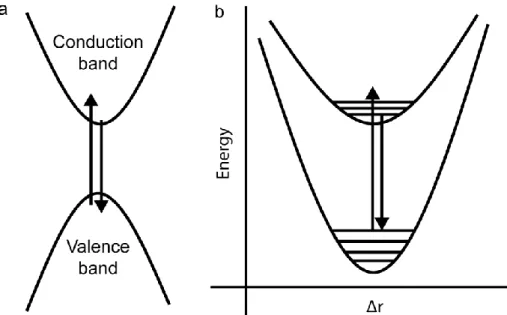
When a lattice supports the formation of localized Frenkel excitons, the resulting exciton- phonon coupling or polaron can severely deform the lattice and immobilize the exciton in the newly generated potential well. This is conceptually different from an exciton becoming trapped in the potential well of a permanent defect (Figure 1.10a), wherein the potential well of the deformation is always present and can be investigated using steady-state methods. In the case of a
self-trapped exciton, the ground-state lattice is the same as that of the perfect, ideal crystal lattice, and the deformation occurs only upon excitation and exciton creation (Figure 1.10b).
Figure 1.10. Self-trapped excitons. a) The trapping of an exciton by a permanent defect; b) an exciton deforming the surrounding lattice to form a self-trapped exciton; c) a CC diagram depicting the absorption and emission from a self-trapped exciton. Reprinted (adapted) with permission from Acc.
Chem. Res. 2018, 51, 3, 619–627. Copyright 2018 American Chemical Society.
In 3D semiconductors such as IV, II-VI, or III-V materials, no self-trapped state exists. Broad emission is therefore from defects or of an extrinsic origin i.e. dopants or impurities. In some 3D lattices such as thallous halides or silver halides, these two states can coexist depending on composition and temperature.89 In other 3D systems, such as alkali halides and doped alkali halides where self-trapped phenomena were first studied and related to the formation of color (F) centers and halide (H) center, the self-trapped exciton is the primary mechanism for PL.8994-95
The tendency for a self-trapped exciton to form in a material depends on two factors: lattice rigidity/deformability and dimensionality.89, 96 These together determine if there is a potential barrier to trapping, how large it might be, and the energy that the lattice may expend when relaxing to the new excited state minimum (top well in Figure 1.10c). The dimensionality of the structure is therefore a critical aspect that can be controlled to influence the electronic properties, the bandgap as well as band-dispersion, the type of exciton that may form, and the luminescence (intrinsically narrow or broad) from the structure.
1.4.3. Two-dimensional metal-halides
2D systems span the entire range of properties based on their thickness and connectivity.97-
98 Systems with thick layers tend to be more planar and behave like their 3D counterparts; as a result, they are more likely to exhibit lower resistivities and possibly the presence of narrow, excitonic emission. This has been demonstrated in several lead-based materials and the Cs2AgBiBr6 double perovskite, most notably in long-chain alkylamines and alkyldiamines.99,100
As mentioned before, systems with very thin layers (e.g. n = 1 or 2) will have larger band gaps (as a result of increased quantum confinement); this was demonstrated by the same group of
authors who also explain the broad emission at low temperatures.96-97, 101 The decreased temperature favors the STE state as there is no longer enough thermal energy to cross the potential barrier that separates FE and STE states.
The connectivity or the construction of these thin layers begins to play a significant role in the height of the thermal barrier and the observed luminescence. 2D systems begin to favor the formation of STEs at higher temperatures through thin-layers and corrugation.97 Corrugation is a structural feature in which the layers are no longer flat planes like those found in the (001) perovskites. Instead, the layers exhibit regular kinks or turns that effectively decrease band dispersion even further and this effectively impedes the transport of charges through the layer and restricts exciton delocalization. These are effectively quasi-2D systems that begin to exhibit STEs at RT and have been demonstrated to emit white light with a PLQY of up to 9%102 or in one case even 17%.103
Although the majority of earlier works on luminescent 2D metal-halides has been conducted on lead-halides,102, 104-111 an increasing body of work has also emerged regarding tin- halides.80-81, 112 Interestingly, these lead-free materials can in some cases have more efficient STE emission as evidenced by their PLQY reaching values over 80%.113-114
The field of quasi-2D and lower dimensional materials is not restricted, as previously mentioned, to materials or elements that can form and stabilize slices or portions of a cubic perovskite framework. These relaxed parameters allow for the exploration of other combinations, and a strict adherence to a divalent or an average divalent B-cation is no longer required although the utilization of ns2 cations is still preferred. Therefore, by utilizing only an M(III) cation (i.e.
Sb3+ or Bi3+) on the B-site, a series of related 2D “3-2-9” structures can be obtained.
Although a structural departure from the perovskite family, these can still be considered in the broader framework of vacancy ordered perovskites in which a 1-1-3 stoichiometry can still be attained. This stems from the fact that the vacancies correspond to one-third of the trivalent metal sites thereby resulting in an overall 3-3-9 ratio of A, B, and X sites.115-116 A greater amount of the corresponding alkali cation must be introduced to charge balance the trivalent cation, and the material adopts a (111) oriented 2D structure (Figure 1.11).117-118
Figure 1.11. The generation of 2D perovskites by removing (100), (110), or (111) planes to generate the corresponding structure. These structures were generated by cutting the respective plane from an ideal structure (based on CaTiO3).
These (111) type structures are found for the majority of A3B2X9 (A = Rb, Cs; B = Sb, Bi; X = Br, I) structures (N.B. Cs3B2I9 forms a 0D structure). The quasi-2D nature of these materials has been demonstrated in Rb3Sb2I9 by its weak, strongly Stokes shifted, broadband RT PL which increases in intensity with cooling and a total lack of narrow excitonic emission.118 Similar observations have been made for the isostructural Cs3B2Cl9 (B = Sb, Bi).119
1.4.4. One-dimensional materials
Further dimensional reduction from the varying types of 2D sheets results in the formation of 1D chains. Here again, the connectivity and chain thickness play a role in dictating the optical properties; however, the number of known structures is lower, and their corresponding optical properties have been investigated to a much lesser degree.120-121 Again, as in the case of 2D metal- halides, 1D Pb-X materials have been studied far more intensively in the past 20 years than their lead-free counterparts.121 As of 2020, at least 21 unique 1D Pb-halides have been discovered and investigated; the structural motifs most commonly include corner-, edge-, and face-shared octahedra.121-136 Although not all have been extensively characterized in terms of their optical properties, several structures have been demonstrated to exhibit broad-STE emission with relatively high QYs at RT.125 This is possible due to the lack of a thermal barrier separating
delocalized Wannier-Mott excitons and localized Frenkel excitons in these systems; as a result, all excitons become trapped and distort the lattice.89
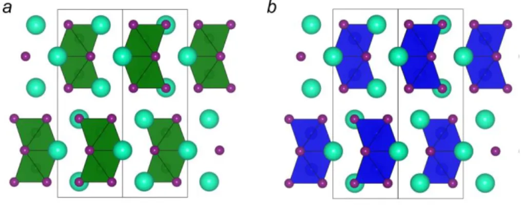
Given these promising results, the investigation into lead-free 1D systems has slowly increased although at the time of writing this dissertation only four luminescent 1D systems have been described in the literature: C4N2H14SnBr4 (Figure 1.12a),137 [C(NH2)3]2SnBr4 (Figure 1.12b),138 (CH3)3SSnI3,139 and (C6H14N2)2[Sb2Cl10]‧H2O.140
Figure 1.12. Luminescent 1D tin-halides: a) C4N2H14SnBr4137, 141 and b) [C(NH2)3]2SnBr4138. Tin- bromide polyhedra are grey with the red-brown spheres representing bromine atoms. The blue and grey lines in a represent the ethylenediammonium cation whereas the brown triangle in b represents the guanidinium cation. In both cases hydrogen atoms have been omitted for clarity.
The former (Figure 1.12a) is composed of chains of edge shared SnBr6 octahedra and is non- emissive at standard temperature and pressure. This material does begin to exhibit broad STE emission once the pressure is increased to 2.06 GPa.125, 141 The underlying mechanism, as explained by the authors, involves a phase transition in which the individual octahedra distort with off-centering of the Sn atom.141 This off centering and octahedral distortion alters the Br-Sn-Br angle further from 180°. This may potentially reduce the orbital overlap between adjacent octahedra and decrease dispersion throughout the chain, effectively dimensionally reducing the 1D chain and enhancing the PLQY. The latter example has intrinsically poor dispersion, which was supported by DFT calculations; this 1D structure may therefore be closer to a pseudo-1D structure. This is furthermore supported by the fact that it exhibits broad yellow emission with a PLQY of 2% at RT, which increases to 75% at 77 K.138
In both cases, these materials have shown the ability to exhibit efficient, broad STE emission when cooled or pressed. This is unlikely to be coincidence, and it is rather symptomatic of a general trend among lead-free metal-halides: dimensional reduction, however it may occur, increases PL.
1.4.5. Zero-dimensional materials
1.4.5.1. Overview
The 0D case represents the limit to this structural disconnection or dimensional reduction.
At this point all the metal-halide building blocks are spatially separated or isolated from one another, and these polyhedra are generally restricted to trimers, dimers, and single isolated polyhedra.
Historically, these phases have received little-to-no widespread attention in the broader scientific community even though the various phases in the ternary metal-halide compositional space have been studied since at least the late 19th century.142-143 Later reports in the mid-20th century observed that the Cs4PbX6 materials, which could form alongside the 3D ABX3
perovskites, exhibited vastly different optical characteristics from their 3D counterparts.144-147 The optoelectronic properties of such 0D phases were not actively investigated further until the latter half of the 20th century with studies on the absorption and conductivity of Sn2+ materials (Cs4SnBr6),148-149 as well as the first studies on the luminescence of 0D Te4+ materials (Cs2TeX6).150 These initial articles focusing on Sn2+ described the both the wide-bandgap and high resistivity that can be expected from these disconnected, 0D structures. The work on Te4+, on the other hand, provided the first look at such materials as phosphors, which exhibit broadband, strongly Stokes-shifted PL at cryogenic temperatures. These initial observations of PL inspired several groups to look deeper at the structures and optical properties of 0D materials with Te(IV), Sb(III), and Bi(III) given their common ns2 electronic configuration. These studies sought to link the ground state crystallographic structure, and the extent to which metal-halide octahedra are disordered, to the PL width and Stokes shift.151-153 Interestingly, they found that these systems are intrinsically broad emitters with varying Stokes shifts and features in the PL spectra based on the strength of exciton-phonon coupling and the degree to which the excited state could distort.
Briefly, more strongly coupled systems would be expected to have more Stokes shifted emission with weaker intensity and less features.154 In general, these studies laid the framework upon which we continue to build and discuss such 0D materials.
Aside from these initial advances, very little has been done prior to 2017 in luminescent materials discovery with only two antimony-chloride based 0D materials effectively characterized.155-156 In fact, the relatively small library of investigated and characterized materials speaks to the young state of this field.157 With the perovskite-era, these 0D curiosities have since undergone renewed interest as their light emission has become an attractive lure. Looking at their structures, several motifs can be identified in most 5s2 and 6s2 metal-halides (Figure 1.13).
Figure 1.13. Structural motifs found in 0D metal-halides: a) polynuclear units, b) mononuclear polyhedra.
The preferred motif for a specific material may affect its tendency to be emissive at RT and is dependent on several factors: metal center, organic vs. inorganic “A” cations, stoichiometry, and lone pair stereoactivity. The metal-center and more specifically its group (i.e. tetrel, pnictogen, chalcogen) has a significant effect on the coordination geometries that it can adopt, mostly as a result of the charge required to maintain the ns2 electronic configuration. These trends are evident in the 5s2 metals viz. Te(IV), Sb(III), Sn(II). The high charge of Te(IV) requires a greater number of ligands to create a stable ternary metal-halide. As a result, the known catalogue of 0D Te(IV) materials is, for the most part, restricted to octahedra (AX6). Sb(III), on the other hand, is able to also adopt geometries containing fewer ligands such as square pyramids (AX5E). Finally, Sn(II), having the lowest charge, adopts these geometries as well as disphenoids or “see-saws” (AX4E).
The adoption of these various geometries in different structures appears to be strongly influenced by the size and structure-directing ability of the “A” cation. Although no general rules or strategies currently exist for the design of structures, it can be observed that coordinatively unsaturated metals are only available via one of two approaches: the selection of large, bulky organic cations or the use of halide anions with very different sizes (e.g. Cl- and I-).157-158 Furthermore, the extent to which these various polyhedra are distorted is associated with a phenomenon known as the lone- pair effect.
This is related to the stereoactivity or the physical presence of the lone pair in a structure.
In coordinatively unsaturated systems such as disphenoids or square pyramids, the lone pair is expressed. In octahedral cases, the expression of this lone pair appears to be correlated with the
underlying symmetry and density of the structure. In high symmetry, fully inorganic systems such as Cs4SnBr6 (or even the 3D CsSnBr3) the octahedra may appear undistorted, masking the lone pair.159 This may be attributed to crystal lattice effects related to site symmetry or the reported interaction of the ns2 pair in this structure with the d-orbitals of the Br-.160 At the opposite end of this spectrum lie the [SnX6]4- octahedra of (C4N2H14)4SnX6, which appear very distorted with bond lengths ranging from 3.17 Å to 3.27 Å.161
As these various factors determine the structural motif adopted by the metal-center, they also determine the appearance or absence of PL at RT and its PLQY. While no general trends exist that can be used to predict the resulting properties of a structure, empirical observations can be drawn from examples in the literature to predict which materials and elements may be the most likely to result in efficient RT emitters. Interestingly, most, if not all, of these motifs have luminescent examples as of 2020. The factors that appear to most often quench PL in these systems are the use of 6s2 cations such as Pb2+ or Bi2+ and heavier halides such as Br- or I-, depending on the system. An excellent set of examples for this comes, in part, from our discoveries in Chapter 2 and Chapter 3 of this dissertation. From these chapters, several A4SnX6 materials can be compared along with their fully inorganic 6s2 counterpart — Cs4PbBr6 (Figure 1.14).
Figure 1.14. The unit cell of Cs4PbBr6.
This material, known since the early 20th century,143, 147 has an aristotypical 0D structure with disconnected [PbBr6]4- octahedra separated by Cs+ cations. The 0D nature of this structure is reflected in its optical and electronic properties, with initial reports describing the material as white (wide bandgap) and very resistive with cryogenic PL in the UV.149, 162-167 This is clearly at odds with recent articles that have erroneously identified this phase as having narrow, green emission, which could be expected from free-exciton recombination but seems highly unlikely for the self- trapped excitonic recombination that should take place in a 0D material.168 More recent reports
![Figure 3.7. Specific sensitivity. The dependence of specific sensitivity on temperature for [C(NH 2 ) 3 ] 2 SnBr 4 (blue), Cs 4 SnBr 6 (green), (C 4 N 2 H 14 I) 4 SnI 6 (red)](https://thumb-eu.123doks.com/thumbv2/1library_info/5332708.1680915/61.918.230.699.411.787/figure-specific-sensitivity-dependence-specific-sensitivity-temperature-snbr.webp)