Co-existence of classical snake states and Aharonov-Bohm oscillations along graphene p-n junctions
P´eter Makk,1, 2,∗ Clevin Handschin,1,† Endre T´ov´ari,2 Kenji Watanabe,3 Takashi Taniguchi,3 Klaus Richter,4 Ming-Hao Liu,5 and Christian Sch¨onenberger1,‡
1Department of Physics, University of Basel, Klingelbergstrasse 82, CH-4056 Basel, Switzerland
2Department of Physics, Budapest University of Technology and Economics, Budafoki ut 8, 1111 Budapest, Hungary
3National Institute for Material Science, 1-1 Namiki, Tsukuba, 305-0044, Japan
4Institut fur Theoretische Physik, Universit¨at Regensburg, D-93040 Regensburg, Germany
5Department of Physics, National Cheng Kung University, Tainan 70101, Taiwan (Dated: April 10, 2018)
Snake states and Aharonov-Bohm interferences are examples of magnetoconductance oscillations that can be observed in a graphenep-n junction. Even though they have already been reported in suspended and encapsulated devices including different geometries, a direct comparison remains challenging as they were observed in separate measurements. Due to the similar experimental signatures of these effects a consistent assignment is difficult, leaving us with an incomplete picture.
Here we present measurements on p-n junctions in encapsulated graphene revealing several sets of magnetoconductance oscillations allowing for their direct comparison. We analysed them with respect to their charge carrier density, magnetic field, temperature and bias dependence in order to assign them to either snake states or Aharonov-Bohm oscillations. Surprisingly, we find that snake states and Aharonov-Bohm interferences can co-exist within a limited parameter range.
INTRODUCTION
Magnetoconductance effects, the change of the con- ductance as a function of magnetic field B, are both of fundamental significance (e.g. Aharonov-Bohm effect, Shubnikov-de-Haas oscillations [1,2]) and important for applications (e.g. GMR [3, 4], TMR [5], etc.). Such ef- fects have been investigated to a great extent also in two dimensional electron gases (2DEGs) realized in semicon- ductor heterostructures [1,2]. At low perpendicular mag- netic fields electrons exhibit cyclotron motion that fol- lows classical trajectories, allowing for the realization of electro-optical experiments such as transverse magnetic focusing [6, 7]. At higher magnetic fields Landau levels are formed and electrons travel along edge channels [1,2].
Using electrostatic gating these channels can be guided within the sample, and using beam splitters based on quantum point contacts electronic Mach-Zehnder inter- ferometers can be realized [8–10]. These interferometers enable the study of coherence effects of electronic states [11–13], noise in collision experiments [14, 15] or prob- ing the exotic nature of certain quantum Hall channels [16,17].
Graphene not only offers similarly high mobility as 2DEGs, but it also allows for 0the formation of gap- less p-n interfaces not possible in conventional 2DEGs.
Graphenep-n junctions host quasi-classical snake trajec- tories at low field [18–23], where electrons curve back and forth along the opposite side of the p-n junction.
At high field edge channels propagate along the junc- tion and coupling between these channels result in a Mach-Zehnder interferometer displaying the Aharonov- Bohm effect [24, 25]. Both effects result in magneto- conductance oscillations as a function of magnetic field
and gate voltage. However, their similar signatures make it difficult to distinguish the two from each other. More- over, experiments are performed within the transition between the classical and the quantum regime. Note that the observation of an Aharonov-Bohm effect requires phase coherent transport, while snake states are based on ballistic transport. Finally, Coulomb interaction of charge carriers localized in conducting islands coupled to edge channels can also lead to magnetoconductance os- cillations [26–29].
Here we present measurements on high-mobility encapsulated graphene p-n junctions, where several sets of magneto-conductance oscillations are observed simultaneously. Related oscillations have been observed [21, 22, 24, 25], but there is still an ongoing discussion on their origin. Their simultaneous observation, which we report here, allows a direct comparison with respect to the gate, field, temperature and bias dependence, resulting in a consistent and comprehensive assignment of the different oscillations.
The paper is organized as follows: First we introduce the most relevant concepts of snake states and Aharonov- Bohm oscillations along graphene p-n junctions. Then we present measurements of several sets of oscillations within the bipolar regime. These magnetoconductance oscillations are carefully analysed with respect to their gate, magnetic field, temperature and bias dependence.
We show that these oscillations can be attributed to ei- ther snake states or Aharonov-Bohm oscillations as in- troduced previously. We furthermore support our find- ings with theoretical models and quantum transport sim- ulations. Finally, we briefly discuss an additional type of magnetoconductance oscillation that has not been re-
arXiv:1804.02590v1 [cond-mat.mes-hall] 7 Apr 2018
2
Classical trajectories
(b)
(c)
(d)
Edge states
N P
x
y λS
N P
VBG I
Vlbg VAC
(e)
N P
N P
(a)
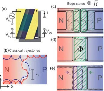
FIG. 1. Concept of snake states and Aharonov-Bohm interference along a graphene p-n junction. a, False- color SEM image of the device where the leads are colored yellow, the graphene encapsulated in hBN is colored cyan and the local bottom-gate (a structured few-layer graphite electrode underneath the hBN-graphene-hBN stack) is col- ored purple . Scale-bar equals 200 nm. VBG denotes the volt- age applied to the global back-gate andVlbg is applied to a graphite bottomgates. b,Snake states seen in the framework of classical skipping orbits for two different magnetic field values (blue and red trajectories, Bred > Bblue). c, Prin- ciple of Aharonov-Bohm interference between quantum Hall edge-states propagating along thep-ninterface. At high bulk filling factors (νL/R) several different areas are enclosed due to inter-channel scattering at the flake edges (green shaded area, and dashed arrows). Of these, the one that involves the least number of scattering events is expected to dominate (Φ1). d, At high magnetic fields Aharonov-Bohm interfer- ence can occur between the spatially separated edge states of the degeneracy-lifted lowest Landau level. The green area corresponds to the insulating region with localνof 0. e,At even larger magnetic fields full degeneracy lifting occurs, and two spin-polarized interferometers are formed: purple area for spin-down (dashed) channels, green for spin-up (solid) chan- nels. The interferometers are independent, as scattering be- tween them is not allowed, since the spin is conserved along the edges.
ported before.
Snake states
In small magnetic fields electrons follow skipping tra- jectories which turn to snake states along the p-n junc- tion [19–22]. These trajectories bend in opposite di- rection on the two sides of the p-n junction due to an opposite Lorentz force, as sketched in Fig. 1b. Charge carriers with trajectories having a small incident an- gle with respect to the p-n junction normal are trans-
mitted very effectively from the n- to p-doped region of the graphene device (and vice versa) due to Klein- tunneling [30–32]. In the simplest case the p-n junc- tion is step-like and symmetric, and the cyclotron radius, RC =λS/2 =~kF/(eB), is the same constant value on both sides. HerekF is the momentum of the electrons,B the magnetic field andλS is the size of the snake period or ”skipping length”. By changing B or the electron den- sity n, and thus the cyclotron radius, the charge carriers end up either on the left or right side of the p-n junc- tion, similar to what is shown in Fig. 1b. This results in a conductance oscillation, where the conductance is determined by how the cyclotron radius compares to the length of thep-n junction.
A more realistic model includes a gradual change of the charge carrier density across the p-n junction, which is illustrated in Fig.1b. For ap-n junction parallel to the y-direction this gives rise to a position-dependent elec- tric fieldE~x (which in the case of constant E-field would lead to the well known E~ ×B~ drift velocity). By solv- ing the semiclassical equations of motion for an idealized graphene p-n junction where the charge carrier density changes linearly fromnLtonRover a distance ofdn, the skipping-lengthλS is given by (see Supporting informa- tion, SI):
λS= π~
eB 2
|nL−nR|
dn . (1)
Note thatS=|nL−nR|/dn corresponds to the slope of the charge carrier density profile. The conductance os- cillations which can be measured across thep-n junction of widthW at a given Fermi-energyE can be described by a phenomenological model according to:
G(E)∼cos
πW λS
, (2)
which describes the commensurability between λS and W. The cosine itself accounts for a smooth conductance oscillation. Details of this model will be discussed later.
We emphasize again that phase coherence is not required for this effect to appear.
Aharonov-Bohm oscillations
While at low magnetic fields the motion of the charge carriers is well described using the picture of skipping and snake trajectories along edges and p-n junctions, upon increasing the magnetic field one enters the quan- tum regime where transport is commonly described by edge states. The concept of interference formed by spa- tially separated edge states has already extensively been studied in 2DEGs, including the realization of Fabry- P´erot [33] and Mach-Zehnder [34] interferometers, while in graphene p-n junctions it was first introduced by
3 Morikawa et al [24]. Here, edge states propagate on ei-
ther side of thep-n junction, and coupling between them is enabled at the junction’s ends due to scattering on dis- ordered graphene edges as illustrated in Fig.1c,d. Cou- pling between the edge states across the p-n junction, illustrated in Fig. 1c by the black, dashed arrows, is re- stricted to the disordered graphene edges [24,25]. As the edge states encircle an enclosed areaA at finite perpen- dicular magnetic field B, the acquired Aharonov-Bohm phase is the magnetic flux, Φ = AB. The conductance oscillations can be described phenomenologically:
G(E)∼cos
2πΦ Φ0
, (3)
where Φ0 =h/e is the magnetic flux quantum [35]. In contrast to snake states, this is a phase coherent effect.
If multiple Landau levels are populated, several differ- ent interferometer loops, enclosing different areas, can contribute. However, for the measured conductance across the p-n junction only paths that connect the n- to the p-side are relevant. Of these, the ones with the least number of scattering events are expected to domi- nate the oscillation. These are the two inner ones denoted with Φ1in Fig. 1c. The interference signal involves only one scattering event along each path, while for loops of type Φ2 at least two scattering events are necessary per path.
At high magnetic fields the Landau levels, which have valley and spin degeneracy at low field, can be partially (or fully) split [36,37]. This leads to a spatial separation of the edge states associated with the lowest Landau level by an insulating region (ν = 0), as shown in Fig. 1d.
Here, the valley degeneracy is lifted so that the edge state is still spin degenerate.
The idea of an Aharonov-Bohm interference, put for- ward in Ref. [24], was generalized by Wei et al. [25] by considering full degeneracy lifting of the Landau levels, both in spin and valley. It was shown that the edges can mix the valleys, but not the spins, as sketched in Fig.1e.
Therefore scattering between edge states is only possible if they are of identical spin orientation. This gives rise to two sets of magnetoconductance oscillations - one for each spin-channel for bulk filling factors|νL/R|>2 as de- scribed in Ref. [25]. An increase of the spacing between neighbouring edge states is expected to decrease the scat- tering rate at the flake edge between edge states, giving rise to a reduced oscillation amplitude. At the same time the magnetic field needed to change the flux by a flux quantum is reduced, which will lead to changing mag- netic field spacing. Details of the magnetic field spacing and the temperature dependence of the Aharonov-Bohm will be discussed later.
MEASUREMENTS
The hBN/graphene/hBN heterostructures were assem- bled following the dry pick-up technique described in Ref. [38]. The full heterostructure was transferred onto a pre-patterned piece of few-layer graphene used as a lo- cal bottom-gate. Standard e-beam lithography was used to define the Cr/Au side-contacts, with the bottom hBN layer (70 nm in thickness) not fully etched through in or- der to avoid shorting the leads to the bottom-gates. The graphene samples were shaped into 1.5µm wide channels using a CHF3/O2 plasma. A false-color SEM image of the final device is shown in Fig.1a (for more details see SI). The charge carrier mobility µ was extracted from field effect measurements yieldingµ∼80 000 cm2V−1s−1. Thep-n junction is formed by a global back- and a lo- cal bottom-gate which allows for independent tuning of the doping on each side of thep-n junction. The pres- ence of Fabry-P´erot oscillations (see SI) also attests to the high quality of our device. We have observed the magnetoconductance oscillations on∼ 10p-n junctions in two separate stacks. Measurements were performed in a variable temperature insert with a base-temperature of T=1.5 K and a He-3 cryostat with a base-temperature of T =260 mK, using standard low-frequency lock-in tech- niques.
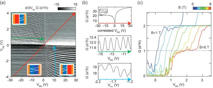
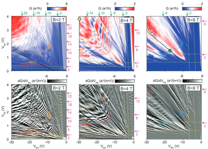
Gate-gate dependence
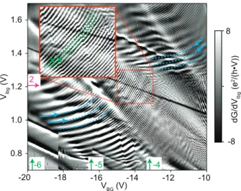
In Fig. 2 the two-terminal conductance (top panels) and its numerical derivative (bottom panels) are shown as a function of the global back-gate (VBG) and the local bottom-gate (Vlbg) within the bipolar regime at selected magnetic fields. Zero voltage of the global back-gate or local bottom-gate corresponds roughly to zero doping in the left or right side of the sample. In the gate-gate map, fine curved lines are visible along which the con- ductance is approximately constant, and perpendicular to these lines the conductance oscillates. Within the measured gate and field range we indentify three differ- ent types of magnetoconductance oscillations which are labelled with red, orange and cyan arrows/dashed lines.
All of them have a roughly hyperbolic line shape being asymptotic with the zero-density lines related to either of the two sides of the samples. However, they are ob- served within different parameter ranges. The filling fac- tors ν = nh/(eB), corresponding to the bulk values of the two sides tuned by the global back-gate and local bottom-gate, are indicated with the green and purple ar- rows in Fig. 2. The yellow dashed lines correspond to
|ν|= 1 and |ν|= 2, for either side.
Upon comparing the different magnetoconductance os- cillations it can be seen that the cyan ones exist at very low filling factors (starting at|ν|>1), the red ones exist at intermediate filling factors (νBG, νlbg) ∼ (−4,4) and
4
2 10
6
B=8 T 6
-30 -20 -10 0
VBG (V)
2
0 2 4
Vlbg (V) 1 3
B=4 T
6 -6
dG/dVlbg (e2/(h•V))
2 6 14 10 18 22
-30 -20 -10 0
VBG (V)
-30 -20 -10 0
VBG (V)
2 6 -2 -6
B=8 T
0 2 4
Vlbg (V) 1 3
2 10 -2 -6 -10 -14
6
B=4 T
2 6 14 -2 -10
10 -18
-26
18 22
B=2 T
2 0
G (e2/h) 0
G (e2/h) 6 0 2
G (e2/h)
6 -6
dG/dVlbg (e2/(h•V)) 6
-6 dG/dVlbg (e2/(h•V))
B=8 T B=2 T
Cut (a)
Cut (b)
FIG. 2.Conductance (top panels) and its numerical derivative (bottom panels) of a p-n junction in the bipolar regime for different magnetic fields. The filling factors, obtained from a parallel-plate capacitor model, are given in green for the cavity tuned by the global back-gate (νBG), and in purple for the cavity tuned by the local bottom-gate (νlbg). The yellow, dashed lines indicate filling factors 1 and 2. The different types of magnetoconductance oscillations are indicated with the red, orange and cyan arrows/dashed curves. The lines indicate where the magnetic field dependencies of Fig.3were taken, whereas the stars indicate the position of the bias dependent measurements of Fig.5.
the orange ones appear at the highest filling factors. For one orange set, the filling factor values where the oscil- lations start to appear are around (νBG, νlbg)∼(−4,8), for the other orange set around (νBG, νlbg) ∼ (−8,4).
Furthermore, the spacing of neighbouring conductance oscillations as a function of charge carrier doping differs significantly for the cyan, red and orange oscillations. An additional conductance modulation is also present where high and low conductance values follow lines that fan out linearly from the common charge neutrality point. The effect is more pronounced at higher magnetic fields and was attributed to valley-isospin oscillations [39–41] which are discussed in detail in Ref. [42].
Whereas for the red magnetoconductance oscillations only one set is observed, two sets are observed for the orange and cyan ones. The latter ones are furthermore shifted in doping with respect to each other. Using a device with a geometry enabling gate defined p-n-p or n-p-n junctions (see SI) we have excluded the possi-
bility that the two orange sets of magnetoconductance oscillations originate from an additional p-n junction formed between n-doped graphene near the Cr/Au con- tacts and a p-doped bulk. This is in agreement with quantum transport simulations (discussed later in this manuscript), which reproduce a double set of oscillations, in the same range where the orange ones are observed, without introducing contact doping. Therefore, a double set of oscillations must be the sign of two different in- terferometer loops working simultaneously near thep-n junction in the bulk (see Fig.1b).
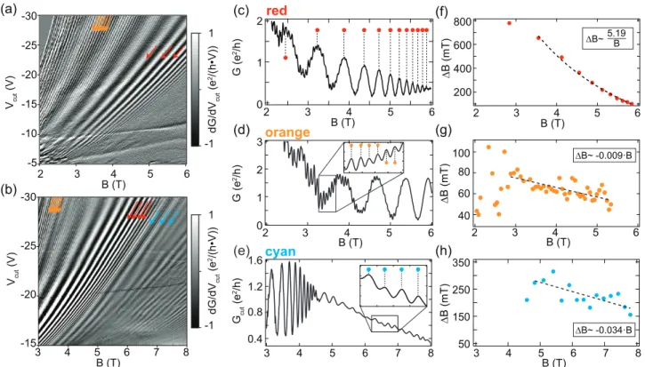
Magnetic field dependence
Next we measured selected linecuts as indicated in Fig.2with “Cut (a)” and “Cut (b)” as a function of mag- netic field. The differential conductances as a function of magnetic field and gate voltage are shown in Fig. 3a,b.
5
3 4 5 6
B (T) -15
-25 -30
Vcut (V) -20
7 8
dG/dVcut (e2/(h•V)) 1
-1
(c)
2 3 4 5
B (T) 6
G (e2/h) 2
0 1
3 4 5
2 6
B (T) 2
1 0 G (e2/h)
(d) 3
3 4 5
2 6
B (T)
(g)
60 40 80
red
orange
(f)
(e)
Gcut (e2/h) 1.6
0.4
3 4 5 6 7 8
(h)
3 4 5 6
B (T) 7 8
cyan
100
∆B (mT)
350 250 150 50
∆B (mT)
166_c7c8_G_vs_small_oscill_01
Vcut (V)
-5 -10 -15 -20 -25
(a)-30
2 3 4 5
B (T) 6
(b)
∆B (mT)
800
200 600 400
2 3 4 5
B (T) 6
∆B~ -0.009·B
∆B~ -0.034·B 5.19B
∆B~
dG/dVcut (e2/(h•V)) 1
-1
1.2 0.8
FIG. 3. Magnetic field dependence. a,Numerical derivative of the conductance as a function of magnetic field and gate voltage as labelled in Fig.2with “Cut (a)”. Within a limited parameter range the magnetoconductance oscillations indicated with the red and orange arrows co-exist. The latter can be better seen inb,along the linecut labelled in Fig.2with “Cut (b)”.c- e,Conductance as a function of magnetic field for representative gate-gate configurations of the red (VBG=−20 V,Vlbg=1.8 V), orange (VBG=−27.5 V,Vlbg=4 V) and cyan (VBG=−18.5 V,Vlbg=1.27 V) magnetoconductance oscillations. The peak-positions are indicated with the red, orange and cyan dots. f-h,Magnetic field spacing between successive peaks (∆B) extracted from (c-e,). A 1/B and linear dependence of∆B as a function of B is indicated with the black dashed curve/lines for the snake states and Aharonov-Bohm interferences, respectively.
The three magnetoconductance oscillations, which are la- belled with the red, orange and cyan arrows, follow a roughly (but not exactly) parabolic magnetic field de- pendence where the oscillations shift to higher absolute gate voltages with increasing magnetic field. Further- more, we observe a co-existence of multiple oscillations within a limited parameter range. The co-existence of the red and orange oscillations is seen in both Fig. 3a and Fig.3b. The conductance as a function of the mag- netic field, while keeping the charge carrier densities on both sides of thep-njunction fixed, is plotted in Fig.3c-e for three selected configurations. In Fig.3c,d large oscil- lations (red in the previous graphs) with peak-to-peak amplitudes reaching nearly 2 e2/h can be seen. Within a limited parameter range there are smaller oscillations (orange in the previous graphs) superimposed on top of the red oscillations, having amplitudes reaching up to
∼0.6 e2/h. The cyan oscillations show amplitudes in the range ∼ 0.05−0.1 e2/h. The magnetic field spacing (∆B) between neighbouring peaks is given in Fig. 3f- h for the corresponding oscillations shown in Fig. 3c-e.
Even though all three types of magnetoconductance os-
cillations reveal a different spacing of∆B, they share a common trend, namely the decrease of∆Bwith increas- ingB. Nevertheless, the rate of∆B as a function of B is quite different for the red compared to the orange and blue magnetoconductance oscillations, which is an indi- cation that different physical mechanism are involved.
Temperature dependence
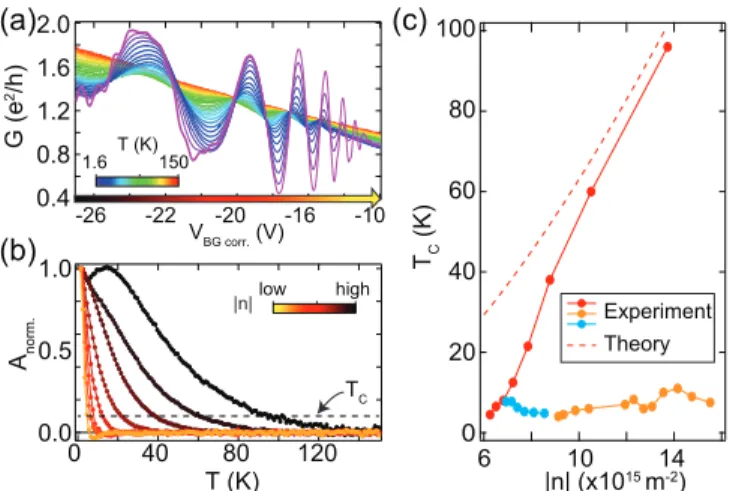
In Fig. 4 the temperature dependence of the red, or- ange and cyan magnetoconductance oscillations is given.
Fig.4a shows the red oscillations as a function of gate voltage and temperature (|nBG| ∼ |nlbg|and B=3.5 T).
We characterize the temperature dependence of each os- cillation by calculating the areaA under the oscillation with respect to the high-T smooth background. From this the normalized area, which is defined as Anorm. = A(T)/A(T = 1.6K), can be extracted at different den- sities, and is plotted as a function of temperature in Fig.4b. A characteristic temperature for the disappear- ance of the oscillations,Tc, is then defined according to Anorm(Tc) = 0.1. In Fig. 4c TC is plotted as a function
6
1.6 1.2 0.8
0.4 -22 -20 -16 -10 G (e2/h)
VBG corr. (V) 2.0
-26
0.00 0.5 1.0
40 80 120
T (K) Anorm.
0 80
TC (K) 40 20
|n| (x1015 m-2)
6 10
60 100
14 Experiment Theory 150
1.6T (K)
high
|n|low
(c) (a)
(b)
TC
FIG. 4. Temperature dependence. a,Red magnetocon- ductance oscillations as a function of the global back-gate (Vlbg is chosen such that|nBG| ∼ |nlbg|) and temperature at B =3.5 T. b, . Anorm of the red oscillations (the dominant ones in (a)) is plotted here as a function of temperature at various densities. The color coding corresponds to the x axis of panel (a). c, The solid lines/dots show the experimental values ofTC, defined as the temperature for which the oscil- lation amplitude is reduced to 10 % of its low temperature value of the red, orange and cyan magnetoconductance oscil- lations (extracted atB =3.5 T, B =3 T andB =8 T respec- tively) as a function of charge carrier doping. The red, dashed line corresponds to the vanishing of snake states according to equation6usingdn=50 nm andW =1500 nm.
of the density for all three types of magnetoconductance oscillations. While the red magnetoconductance oscilla- tion reveals a significant temperature dependence as a function of the charge carrier density, surviving up to T ∼100 K at high doping, the orange and cyan magneto- conductance oscillations vanish at temperatures around T ∼10 K irrespective of the charge carrier density. This suggests again that different mechanisms are responsible for the red magnetoconductance oscillations compared to the orange and cyan magnetoconductance oscillations.
Ballistic effects, such as snake states and transverse mag- netic focusing, are known to survive to temperatures up to T ∼100 K to 150 K [7, 22, 43]. On the other hand, phase coherent transport in similar devices vanishes at temperatures around∼10 K (see Ref. [44]).
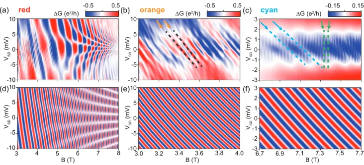
Bias dependence
We have also investigated the bias dependence of the different oscillations as a function of magnetic field while keeping the charge carrier densities fixed. The bias was applied asymmetrically at the source, while the drain re- mained grounded. The red magnetoconductance oscilla- tions evolve from a tilted line pattern at smaller magnetic fields into a checker-board pattern at high magnetic field as shown in Fig.5a (a smooth background is subtracted).
At high magnetic field the visibility of the checker-board pattern decreases with increasing VSD while a similar behaviour is absent (within the applied bias range of
±10 mV) for the tilted pattern. The bias dependence of the orange and cyan magnetoconductance oscillations is shown in Fig.5b,c, both revealing a tilted line pattern within the measured magnetic field range, as shown by the dashed lines and arrows. The bias dependence of the orange oscillations persists to ±10 mV, whereas that of the cyan oscillations vanishes around roughly±2 mV. In Fig.5c additional magnetoconductance oscillations with a narrow spacing of roughly∆B∼4 mT to 6 mT can be observed, indicated by green arrows and green dashed lines. These oscillations will be briefly discussed at the end of the paper.
DISCUSSION
We have observed different magnetoconductance oscil- lations, marked with red, orange and blue. All of the oscillations have a roughly hyperbolic line shapes in the gate-gate map, but the magnetic field spacing, the tem- perature dependence and the fact that there is only a sin- gle set of red oscillations suggest that they are governed by different physical mechanisms. Based on the experi- mental evidence presented until now, it is suggestive to assign the red oscillations to snake states and the others to the Aharonov-Bohm effect. This will be substantiated further on below.
Magnetoconductance oscillations marked in red The red magnetoconductance oscillations start to ap- pear in the range |ν| ∼ 3−6 as can be seen in Fig. 2.
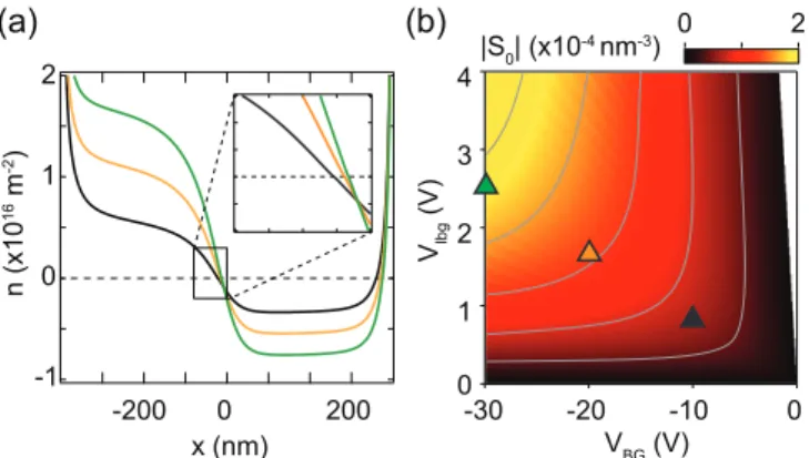
This corresponds to an occupation of roughly two edge states (ν = ±4, Landau levels 0 and ±1) without tak- ing degeneracy lifting into account. The shape of the red magnetoconductance oscillations fits very well to what is expected for snake states following equation1and equa- tion2, as we will show below.
As discussed in the introduction, the oscillation results from a commensurability relation of the p-n junction length and the skipping length, where the conductance is high or low depending on whether the snaking tra- jectories end up on the source or the drain side. If the magnetic field is fixed, the skipping-lengthλS is directly proportional to the slope of the p-n junction according to equation 1. In Fig. 6a the calculated charge carrier density profile atB =0 T is shown for three exemplary gate-gate configurations (details of the electrostatic sim- ulations are given in the SI). It is clear that S0 charac- terizes well the density profile in the vicinity of thep-n junction. S0 as a function of gate voltages is plotted in Fig.6b: here curves of constantS0, and therefore of
7
VSD (mV) -10
10
-5 0 5
4 7
B (T) 5
3 3.4 4.0
B (T) 3.2
3.0 3.6
(a)
VSD (mV) -10
10
-5 0 5
6 8 3.8
red ∆G (e2/h) -0.5 0.5
VSD (mV) -10
10
-5 0 5
(b) orange ∆G (e2/h) -0.5 0.5
VSD (mV) -10
10
-5 0 5
B (T)
(c) cyan ∆G (e2/h) -0.15 0.15
VSD (mV) -2
0 1 -1 3
VSD (mV) 2
-3
-2 0 1 -1 3 2
-36.7 6.9 7.1 7.3 7.5 7.7
(d) (e) (f)
FIG. 5. Bias spectroscopy. a-c Measurement of the red, orange and cyan magnetoconductance oscillations as a function of bias and magnetic field where a smooth background was subtracted. Gate-voltages remain fixed and are indicated in Fig. 2 with the yellow (red and orange oscillations) and green (cyan oscillation) stars. d-f, Phenomenological simulations of the bias dependence of snake state and interference-induced oscillations(a-c). Parameters used: W =1.5µm, dn =100 nm (red oscillations), kF corresponding to n ∼1.7×1012cm−2 (red, orange) or n ∼0.8×1012cm−2 (cyan). For the Aharonov- Bohm oscillations we considered a bias dependent gating effect withα=0.32 nm/mVSD andd=40 nm (orange oscillation) or α=0.25 nm/mVSD andd=20 nm (cyan oscillations), while a renormalization of the edge state velocity is neglected (β= 1).
constantλS(ifB remains fixed), follow a roughly hyper- bolic line shape in agreement with the shape of the red magnetoconductance oscillations (Fig.2). Although the orange and cyan oscillations also seem to follow hyper- bolic shapes on gate-gate maps, the red ones only have a single set as expected of snake states.
Next we analyze the magnetic field dependence and spacing expected of snake state induced oscillations.
Based onS0(Fig.6b) one can calculate the conductance contribution as a function of an arbitrary linecut and magnetic field (not shown here), leading to a roughly parabolic magnetoconductance oscillation which strongly resembles the measurements shown in Fig.3a,b.
By using the model with a constant density gradient the magnetic field spacing as a function of magnetic field is given approximately by (see SI):
∆B∼2π2~2n e2W dn
1
B, (4)
where a symmetricp-njunction withn≡ |nL|=|nR|was assumed. The magnetic field spacing in the experiment is very well described by the 1/B dependence. By fit- ting the magnetic field spacing of the snake state model as described in equation 4 to the measurements shown in Fig.3f we extracted a slope of S =1.82×10⁻³nm−3 which is roughly one order of magnitude larger than what was calculated in Fig. 6b (S0 ∼1.2×10⁻⁴nm−3). One explanation for the discrepancy is that strictly speaking
S0 is only valid at B =0 T. However, at finite mag- netic field the charge carrier density has to be calculated self-consistently leading to areas with a constant charge carrier density (compressible region) and areas where the charge carrier density changes rapidly (S > S0, incom- pressible regions) [45]. Also, the model supposes that the trajectories stay within the area with a constant density slope (see SI), which might be not valid at low fields due to the increased cyclotron radius and skipping length.
The decrease of the oscillation amplitude with increas- ing magnetic field (Fig.3c) is compatible with the picture of classical snake trajectories, where the conductance os- cillation results from the sum over all trajectories which form caustics along thep-n junction [46, 47]. Upon in- creasing the magnetic field the charge carriers have to pass thep-n junction more often (decreasing λS). This leads to a reduced oscillation amplitude [23] because only trajectories with an incident angles being perpendicular to thep-n junction (θ = 0) have a transmission proba- bility oft = 1, while for all remaining trajectoriest <1 is valid [31,32,48].
Our most compelling argument for identifying the red os- cillations with snake states comes from the comparison of the measured temperature dependence with that cal- culated by the following simple model. At finite temper- aturesT the Fermi-surface is broadened by ∆E ∼kBT (where kB is the Boltzmann constant), thus leading to a spread of the Fermi-wavevector according to ∆kF ∼
8 (b)
0 2 4
Vlbg (V) 1 3
-30 -20 -10 0
VBG (V)
2
|S0| (x10-4 nm-3) 0
(a)
1 0 -1 n (x1016 m-2)
0 x (nm) 2
-200 200
FIG. 6. Charge carrier density profile in the bipolar regime and extracted slope. a, Representative charge carrier density profiles calculated from electrostatics at posi- tions as indicated in (b) with the triangles. Atn= 0 the slope is nearly linear (inset). b,Slope|S0|extracted atn= 0 as a function of the gates. Grey curves represent constant values of|S0|, and consequently ofλS, as well (equation1).
kBT /(~vF). The oscillations are expected to vanish if the smearing of trajectories becomes comparable to half a period:
2 (λS,max−λS,min)·N ∼ hλSi, (5) whereλS,max,λS,minandhλSicorrespond to the maximal, minimal and average skipping-length, respectively and N to the number of skipping periods. This leads to a characteristic temperature
Tc≈ 2vF~3 W dnkBe2B2
√n3π5, (6)
where the oscillations vanish. HerekB is the Boltzmann constant. Details of the calculation can be found in the SI. The vanishing of the red magnetoconductance oscil- lations with increasing charge carrier doping, which is plotted in Fig. 4c (red, dashed line), is in good agree- ment with what is expected for snake states according to Equation6, unlike the other type of oscillations.
Finally, we analyze the bias dependence of snake states.
Details of the model can be found in the SI. The bias de- pendence is calculated by taking into account the energy dependence of the snake-period through its momentum dependence. In the case of a fully asymmetric bias the model reproduces the tilted pattern which is shown in Fig.5d at low magnetic field. On the other hand, for the case of completely symmetric bias, the same model leads to the checker-board pattern which is shown in Fig. 5d at high magnetic field. The checker-board pattern is in agreement with previous studies [24, 25], where a simi- lar behaviour was observed. The oscillation period de- creases with increasing magnetic field in the simulation (Fig.5d) comparable to the experiment (Fig.5a). In or- der to reproduce the transition from tilted (asymmetric
biasing) to checker-board pattern (symmetric biasing) we varied the bias asymmetry going from low to high mag- netic field. We speculate that it might be related to the capacitances in the system [49], but the precise reason remains unknown so far. We discuss this in more detail in the SI.
Magnetoconductance oscillations marked in orange From all the observed magnetoconductance oscillations the orange ones occur at the highest filling factors start- ing at roughly|ν| ∼ 6 and persisting up to|ν| = 20 or even higher, as shown in Fig. 2. This corresponds to an occupation of at least two edge states (|ν| = 0 and
|ν|= 4) without taking a possible degeneracy lifting into account. Snake states can be excluded here, as the dou- ble set of oscillations indicates two simultaneous effects, with their origin displaced in real space with respect to thep-n junction. Therefore, we attribute these oscilla- tions to Aharonov-Bohm oscillations between quantum Hall edge states propagating in parallel with each other and the p-n junction. Their temperature, B-field and bias dependence also support this idea. Below we discuss expectations and compare them with our experimental observations.
In an Aharonov-Bohm interferometer, the magnetic field spacing∆Bbetween neighbouring conductance peaks is given by:
∆B= h e 1
A. (7)
Here Φ0=h/e is the magnetic flux quantum andAis the enclosed area given by the product of the width of the flakeW and the distance of the edge states,d.
This suggests a constant ∆B for a fixed spacing d.
However, in the experiments∆Bis not exactly constant because the real-space positions of the edge states, which defineA, vary as a function of magnetic field and thep- n junction’s density profile [24]. By considering a linear charge carrier density profile∆Bdecreases linearly with increasingB. This is in agreement with what was mea- sured in Fig.3g,h, indicated with the black dashed line, therefore suggesting an Aharonov-Bohm type of inter- ference. Even though multiple areas might be enclosed between the various edge states, only one Aharonov- Bohm loop will dominate as explained previously and sketched in Fig.1b. The magnetic field spacing of the or- ange magnetoconductance oscillations (Fig.3g) was con- verted into a distance ranging fromd∼30 nm at B∼2 T tod∼55 nm atB∼5.5 T. The decreasing oscillation am- plitude (∆Gosc) with increasing magnetic field (Fig. 3d) directly indicates the vanishing coupling between edge states as they move further apart from each other at higher magnetic fields.
We have used the zero-field electrostatic density profile
9 shown in Fig. 6a to identify the spacing d between two
edge state for any set of (VBG,Vlbg) within the gate-gate map. The magnetoconductance oscillation can then be calculated according to equation3, leading to a roughly hyperbolic shape as a function of the two gates at fixed magnetic field (see Supporing Informations). The two sets of the orange oscillations can be reproduced with a double Aharonov-Bohm interferometer as sketched in Fig.1b, where the conductance oscillations arising from the interferometer on the left (e.g. quantum Hall chan- nel with ν = 0 and ν = ±4) and right (e.g. ν = 0 and ν = ∓4) side are added up incoherently. The two sets of orange magnetoconductance oscillations are slightly shifted in doping with respect to each other because each of the two gates tunes one side of thep-n junction more effectively. Furthermore, measuring a linecut as a func- tion of magnetic field reveals a roughly parabolic trend (see SI). These findings are in good agreement with the measurements which are shown in Fig. 2 and Fig. 3a,b, respectively.
In interference experiments which depend on phase co- herent transport, a vanishing of the oscillation pattern with temperature can have different origins such as loss of phase coherence due to enhanced inelastic scattering events. As soon aslΦ< L, wherelΦis the phase coher- ence length andL is the total path length, the interfer- ence pattern is almost completely lost. As mentioned be- fore, the phase coherence length is below 1−2µm in simi- lar devices at temperatures around∼10 K (see Ref. [44]).
However, the interference can as well be lost at finite tem- peratures even iflΦ> Lif the two interfering paths have different lengths (∆L 6= 0), again due to the smearing of the Fermi wavevector. In this case, the interference pattern is expected to vanish at temperatures around
T = hvF
kB∆L. (8)
Since for the Aharonov-Bohm interference along a graphenep-n junction∆Lis ideally zero (see Fig.1b,c) or very small, this effect is negligible. Consequently, the loss of the interference signal with increasing tempera- ture depends on the decrease of lΦ, which depends only weakly on the charge carrier doping [44], in agreement with Fig.4c.
Finally, we calculate the bias dependence of Aharonov- Bohm oscillations. The details of the model are discussed in the SI. The bias dependence is introduced via the mo- mentum difference which leads to:
G(V)∼cos
2πW ·(d+αV)·B
Φ0 +k∆L
. (9) Here αis a phenomenological parameter in order to ac- count for a bias dependent gating effect [11]. For sim- plicity the edge state spacingdis modified proportional to the applied bias. The factor k∆L in Equation 9 ac- counts for a possible path-difference between the edge
states, wherekis replaced byk=kF+eV /(~vFβ). The parameter β (0 ≤ β ≤ 1) was introduced to account for the renormalized edge state velocity compared to the Fermi velocity [50].
We have found that the second term alone (k∆L at α = 0) cannot lead to substantial bias dependence if the parameters are chosen realistically (∆L∼20 nm and β = 1). To account for the tilt of the measurement a considerable renormalization of the edge state velocity is needed leading to an unphysically large reduction ofvF
by a factor of one hundred. Therefore most of the tilt must come from non-zeroαand the bias induced gating effect.
The applied bias voltage shifts the electrochemical po- tential on one side (or both sides) and therefore leads to a change of the density profile. The changing den- sity profile results in shifting of the edge states, and in order to keep the flux through the interferometer fixed, the magnetic field has to be changed. Assuming that the applied bias affects the edge state spacing according to
∆d=α·VSD, thenαcan be extracted from the bias spac- ing in Fig.5b. This leads to values ofα∼0.32 nm/mVSD. The resulting bias dependence is plotted in Fig.5e. Based on a simple model, it is possible to numerically estimate the value of alpha, to compare with the observation. We keep the widthdn of thep-n junction constant, and take the bias voltage into account directly changing the left and right band offset and thusnL/R. From this simple model we obtain values in the order ofα∼0.39 nm/mVSD
to 0.48 nm/mVSDfor the orange magnetoconductance os- cillations, which agrees fairly well with the experimental observations. Details are given in the SI.
Magnetoconductance oscillations marked in cyan The cyan magnetoconductance oscillations were ob- served at the lowest filling factors as low as |ν| ∼ 2 or even less, above B ∼4 T as shown in Fig. 2. We at- tribute these oscillations to Aharonov-Bohm oscillations formed by edge channels of the fully degeneracy lifted lowest Landau level, as shown in Fig.1e). Since full de- generacy lifting of the lowest Landau level (valley and spin) is observed forB >5 T (see SI), the edge states are spin and valley polarized. While the spin degree of free- dom is conserved along the edges of graphene and along thep-n junction [25], the valley degree of freedom is only conserved along the p-n junction. Mixing between the edge states of the lowest Landau levels having equal spin is consequently prohibited along the p-n junction, but possible at the graphene edges. Comparable to the or- ange magnetoconductance oscillations, the magnetic field spacing of the cyan oscillations decreases monotonically, corresponding to an edge state spacing of d ∼9 nm at B =4.5 T and to d ∼15 nm at B =8 T. The oscilla-
10 (a)
0 2 4
1 3
-30 -20 -10 0
VBG(V)
2 6
-2
Vlbg(V)
T 0 2.5 (b)
-10 -20 -30
2 4 5
B (T) Vgate(V)
T 0 4
B=3 T
10 14
-10 -18
3 -15
-25
FIG. 7. Quantum transport calculations for a graphene p-n junction in magnetic field. a,Transmis- sion function (T) of charge carriers through thep-njunction with the same gate geometry as measured one, as a function of a local bottom-gate and a global back-gate. Red and or- ange magnetoconductance oscillations are indicated with the dashed curves/arrows. Filling factors of the global back-gate and the local bottom-gate are indicated with the green/purple arrows. Low doping values (shaded in grey) were omitted to reduce the computational load. b,Linecut as indicated in (a) with the black line as a function of magnetic field.
tion amplitude of the cyan magnetoconductance oscilla- tion shown in Fig.3c was rather constant with magnetic field including some irregularities. We note that the cyan magnetoconductance oscillations are predominantly vis- ible at a charge carrier doping of |nBG| ∼ |nlbg| (Fig.2) for reasons which are unknown yet. Similar to the or- ange magnetoconductance oscillations, the temperature dependence of the cyan ones depends only slightly on the charge carrier density, and is most likely related to the loss of phase coherence.
Finally, the bias dependence is modelled similarly to the orange oscillation. The measurements can be well re- produced by usingα∼0.25 nm/mVSDto account for the bias dependent gating effect as demonstrated in Fig.5f, which shows good agreement with our measurements (panel c). Our simple estimate using the model detailed in the SI gives values in the order ofα∼0.16 nm/mVSD
to 0.25 nm/mVSD for the cyan magnetoconductance os- cillations, again agreeing fairly well with the experimen- tal findings.
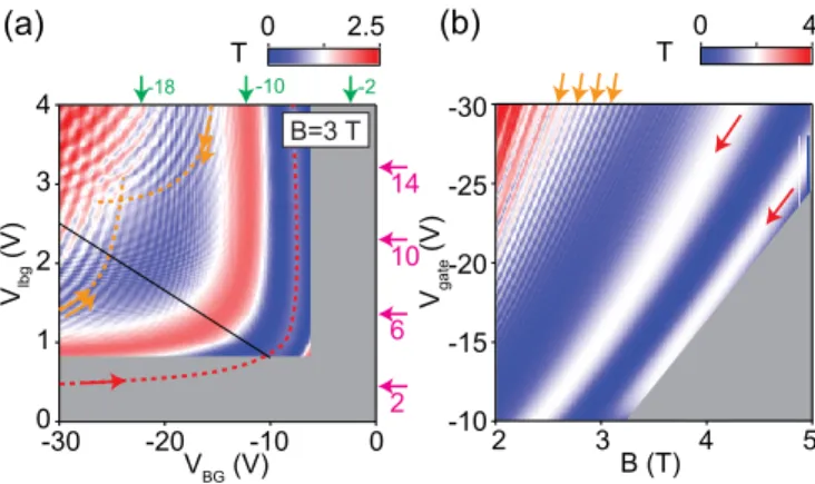
QUANTUM TRANSPORT SIMULATIONS To complement our measurements, we additionally performed quantum transport calculations based on so- called scaled graphene [51] using the realistic device ge- ometry. These calculations were able to reproduce the red and orange magnetoconductance oscillations. In the calculations electron-electron interactions is not taken into account. In Fig. 7a the conductance is shown as
a function of the local bottom-gate and the global back- gate atB=3 T within the bipolar regime. Comparable to the measurements presented in Fig.2, two sets of magne- toconductance oscillations can be seen which are shifted in doping, which we identify with the orange ones. A few ridges also appear which we assign to the red oscil- lations. In Fig. 7b the evolution of the red and orange oscillations are shown as a function of gate and magnetic field. The calculations show that the orange magneto- conductance oscillations seen in the experiments can be reproduced without the splitting of the lowest Landau level in contradiction with the claims of Ref. [25]. In that work all oscillations were linked to the split lowest Landau levels, however our analysis shows that only the blue oscillations, appearing at the lowest filling factors, can be attributed to degeneracy lifted Landau levels.
ADDITIONAL MAGNETOCONDUCTANCE OSCILLATIONS AT HIGH MAGNETIC FIELD
Two additional sets of magnetoconductance oscilla- tions which that have been observed already in Fig.5c are shown in detail in Fig.8, marked in green. Detailed gate, magnetic-field, temperature and bias dependence is shown in the SI. The gate spacing is much shorter than for other osccilations (see SI). From magnetic field depen- dent measurements, spacing of∆B =6 mT atB =5.8 T to ∆B =4 mT at B =8 T have been extracted. How- ever, the magnetic field spacing of the second set of green magnetoconductance oscillations yields different values, ranging from∆B=25 mT at B=6 T to∆B∼10 mT at B=8 T. The bias and temperature dependent measure- ments show vanishing oscillations aroundVSD ∼±1 mV andT ∼2 K to 3 K.
The origin of these oscillations is unknown. Aharonov- Bohm oscillations would correspond to an edge state spacing as high as∼700 nm, which is clearly unphysically large. The combination of edge states and a charge car- rier island co-existing in the device could lead to Coulomb blockade oscillations. However, gate and magnetic-field spacings give inconsistent island sizes. Details and more discussions are given in the SI. To resolve the origin of these oscillations further studies are needed.
CONCLUSION
In conclusion, we have observed three types of magne- toconductance oscillations in transport along a graphene p-n junction. We have demonstrated from the detailed analysis of the various oscillations that both snake states and Aharonov-Bohm oscillations appear within our mea- surements, and even co-exist in some parameter region.
The question arises: how can a snake state, mostly imag- ined as a classical ballistic trajectory, exist in the regime
11
8
-8
VBG (V)
dG/dVlbg (e2/(h•V)) 1.2
1.6
Vlbg (V) 1.0 1.4
-16 -14 -12 -10
-20 -18
0.8
-6 -5 -4
2
FIG. 8. Additional magnetoconductance oscillations at high magnetic field. Numerical derivative of the con- ductance as a function of the global back- and local bottom- gates at B =8 T where two additional sets fine oscillations can be observed (indicated with the green, dashed line)), su- perimposed on each set of cyan oscillations. Left and right side filling factors are indicated by green and purpler arrows, respectively.
where quantum effects also seem to be present, as demon- strated by Aharonov-Bohm interferences? Here we pro- vide a comprehensive picture of both effects.
(1) By investigating the gate-gate maps we have seen that first, at the lowest densities and largest magnetic fields, Aharonov-Bohm oscillations originating from sym- metry broken states appear. In this case no coupling be- tween the edge states is present along the p-n junction, only at the flake edges. At low doping the slope of the po- tential profile, and hence the electric field is small, which results in spatially separated edge channels which can only mix at the flake edge. This Aharonov-Bohm effect has been recently studied in Ref. [25], and modeled as two edge channels with different momentum along thep- n junction. The Aharonov-Bohm flux can be calculated from the momentum difference of edge channels, as it is directly related to their guiding center [52].
(2) As the bulk doping and hence the electric field is further increased, the edge-states propagating along the p-n junctions are no longer eigenstates and start to mix.
This effect has been studied previously for constant elec- tric field, where it has been shown that forEc> vF ·B, mixing of the states occur, and electrons can cross the p-n junction [53–55]. In the very recent calculations of Cohnitz et al. in Ref. [50], it has been shown, that in this regime interface modes, with velocity corresponding to classical snake states appear. The real space motion of the center of the wavepackage, that gives rise to the snake movement along thep-n junction, can thus be un- derstood as an emergent spatial oscillations inherent in
the modulus of the true energy eigenstate, which due to the mixing is a superposition of edge states on the left and right of thep-n junction. In the simplest picture, one has a superposition of one mode on the left and one on the right that are coupled through the electric-field. This results into a periodic motion in real space mimicking snake-orbits with the effect of a periodic oscillations in the conductance which corresponds to the classical com- mensurability criterion. A simple model demonstrating this is given in the SI. The oscillation frequency depends on the potential strength and cyclotron frequency. The situation in our sample is more complex, since there are several channels and the electric field is position depen- dent: it is largest at the center of the p-n junction and decreases further away from it. In addition, the magnetic field further complicates electrostatics due to the forma- tion of Landau levels in the density of states. This makes quantitative analysis very challenging. Similar pictures based on numerical analysis have been presented in Refs.
[20, 23]. Further details on this model will be given in the SI.
(3) Finally as the density is increased further other oscillations appear, marked by orange. We attribute them to Aharonov-Bohm oscillations between the lowest Landau levels, i.e. the inner-most edge states at the center of the p-n junction. For these edge state on can find two interfering paths for which only one nearest-neighbor edge scattering along the graphene edge is needed to define an interference loop. Though higher order edge-states may contributes as well, there magnitude are much smaller, since to connect these states in an Aharonov-Bohm path that reaches from one side of the p-n junction to other will require more than one scattering event giving rise to a very small visibility. Let us emphasize the different origins of the snake-state and Aharonov-Bohm oscillations: the former are caused by edge-state mixing in the bulk due the presence of a strong electric field, while the later rely on scattering along the graphene edge caused by edge disorder. We also stress that the orange magnetoconductance oscillations can be reproduced nearly perfectly using quantum transport simulations, without including electron-electron interactions or a Zeeman-term. Therefore we can exclude partial or full degeneracy lifting of the lowest Landau level in order to explain the orange oscillations.
Our study made the large steps in understanding the complex behaviour graphene p-n junctions observed on the boundary of quasi-classical and quantum regime, and showed the surprising finding that Aharonov-Bohm like interferences and quasi-classical snake states can co-exist. Future studies might focus on the origin of the transition between tilted and checker-board pattern in the bias-dependence of the snake states. In further steps interferometers based on bilayer graphene can be
12 constructed, where electrostatic control of edge channels
is possible. Recent works have shown the potential to engineer more complex device architectures [56, 57], where also exotic fractional quantum Hall states could be addressed.
Acknowledgments
The authors gratefully acknowledge fruitful discus- sions on the interpretation of the experimental data with Peter Rickhaus, Amir Yacobi, L´aszl´o Oroszl´any, Rein- hold Egger, Alina Mrenca-Kolasinska, Csaba T˝oke and thank Andr´as P´alyi for discussion ons the quantum snake model presented in the SI. This work has received fund- ing from the European Union Horizon’s 2020 research and innovation programme under grant agreement No 696656 (Graphene Flagship), the Swiss National Science Foundation, the Swiss Nanoscience Institute, the Swiss NCCR QSIT, ISpinText FlagERA network and from the OTKA PD-121052 and OTKA FK-123894 grants, and K.R and M.H.L. from the Deutsche Forschungsgemein- schaft (project Ri 681/13). P.M. acknowledges support from the Bolyai Fellowship. Growth of hexagonal boron nitride crystals was supported by the Elemental Strat- egy Initiative conducted by the MEXT, Japan and JSPS KAKENHI Grant Numbers JP26248061, JP15K21722, and JP25106006.
∗ These authors contributed equally; Pe- ter.makk@unibas.ch
† These authors contributed equally
‡ Christian.Schoenenberger@unibas.ch
[1] T. Ihn, Semiconductor Nanostructures (Oxford Univer- sity Press, 2010).
[2] Y. V. Nazarov and Y. M. Blanter, Quantum Transport:
Introduction to Nanoscience(Cam, 2012).
[3] M. N. Baibichet al., Phys. Rev. Lett.61, 2472 (1988).
[4] G. Binasch, P. Gr¨unberg, F. Saurenbach, and W. Zinn, Phys. Rev. B39, 4828 (1989).
[5] M. Julliere, Phys. Lett. A54, 225 (1975).
[6] H. van Houtenet al., Phys. Rev. B39, 8556 (1989).
[7] T. Taychatanapat, K. Watanabe, T. Taniguchi, and P. Jarillo-Herrero, Nat Phys9, 225 (2013).
[8] Y. Jiet al., Nature422, 415 (2003).
[9] P. Samuelsson, E. V. Sukhorukov, and M. B¨uttiker, Phys.
Rev. Lett.92, 026805 (2004).
[10] I. Nederet al., Nature448, 333 (2007).
[11] E. Bieriet al., Phys. Rev. B79, 245324 (2009).
[12] L. V. Litvin, H.-P. Tranitz, W. Wegscheider, and C. Strunk, Phys. Rev. B75, 033315 (2007).
[13] E. Bocquillonet al., Science339, 1054 (2013).
[14] M. Hennyet al., Science284, 296 (1999).
[15] W. D. Oliver, J. Kim, R. C. Liu, and Y. Yamamoto, Science284, 299 (1999).
[16] A. Bid, N. Ofek, M. Heiblum, V. Umansky, and D. Ma- halu, Phys. Rev. Lett.103, 236802 (2009).
[17] D. E. Feldman and A. Kitaev, Phys. Rev. Lett. 97,
186803 (2006).
[18] J. R. Williams and C. M. Marcus, Phys. Rev. Lett.107, 046602 (2011).
[19] M. Barbier, G. Papp, and F. M. Peeters, Appl. Phys.
Lett.100, 163121 (2012).
[20] Milovanovi´c, M. Ramezani Masir, and F. M. Peeters, Appl. Phys. Lett.105, 123507 (2014).
[21] P. Rickhauset al., Nat Commun6, 6470 (2015).
[22] T. Taychatanapatet al., Nat Commun6, 6093 (2015).
[23] K. Kolasi´nski, A. Mre´nca-Kolasi´nska, and B. Szafran, Phys. Rev. B95, 045304 (2017).
[24] S. Morikawaet al., Appl. Phys. Lett.106, 183101 (2015).
[25] D. S. Weiet al., Sci Adv3(2017).
[26] Y. Zhanget al., Phys. Rev. B79, 241304 (2009).
[27] S. Ilaniet al., Nature427, 328 (2004).
[28] B. I. Halperin, A. Stern, I. Neder, and B. Rosenow, Phys.
Rev. B83, 155440 (2011).
[29] E. Tovari, P. Makk, P. Rickhaus, C. Schonenberger, and S. Csonka, Nanoscale8, 11480 (2016).
[30] O. Klein, Z. Phys.53, 157 (1929).
[31] V. V. Cheianov and V. I. Fal’ko, Phys. Rev. B74, 041403 (2006).
[32] M. I. Katsnelson, K. S. Novoselov, and A. K. Geim, Nat Phys2, 620 (2006).
[33] C. de C. Chamon, D. E. Freed, S. A. Kivelson, S. L.
Sondhi, and X. G. Wen, Phys. Rev. B55, 2331 (1997).
[34] Y. Jiet al., Nature422, 415 (2003).
[35] Y. Aharonov and D. Bohm, Phys. Rev.115, 485 (1959).
[36] Y. Zhanget al., Phys. Rev. Lett.96, 136806 (2006).
[37] A. F. Younget al., Nat Phys8, 550 (2012).
[38] L. Wanget al., Science342, 614 (2013).
[39] J. Tworzyd lo, I. Snyman, A. R. Akhmerov, and C. W. J.
Beenakker, Phys. Rev. B76, 035411 (2007).
[40] T. Low, Phys. Rev. B80, 205423 (2009).
[41] Q. Ma, F. D. Parmentier, P. Roulleau, and G. Fleury, arXiv:1801.02235 (2018).
[42] C. Handschinet al., Nano Lett.17, 5389 (2017).
[43] M. Leeet al., Science353, 1526 (2016).
[44] S. Zihlmann, P. Makk, K. Watanabe, T. Taniguchi, and S. Sch¨onenberger, To be published.
[45] D. B. Chklovskii, B. I. Shklovskii, and L. I. Glazman, Phys. Rev. B46, 4026 (1992).
[46] N. Davieset al., Phys. Rev. B85, 155433 (2012).
[47] A. A. Patel, N. Davies, V. Cheianov, and V. I. Fal’ko, Phys. Rev. B86, 081413 (2012).
[48] S. Chenet al., Science353, 1522 (2016).
[49] D. T. McClure et al., Phys. Rev. Lett. 103, 206806 (2009).
[50] L. Cohnitz, A. De Martino, W. H¨ausler, and R. Egger, Phys. Rev. B94, 165443 (2016).
[51] M.-H. Liuet al., Phys. Rev. Lett.114, 036601 (2015).
[52] T. Stegmann, D. Wolf, and A. Lorke, New J. Phys.15, 113047 (2013).
[53] V. Lukose, R. Shankar, and G. Baskaran, Phys. Rev.
Lett.98, 116802 (2007).
[54] A. Shytov, M. Rudner, N. Gu, M. Katsnelson, and L. Levitov, Solid State Communications 149, 1087 (2009).
[55] A. V. Shytov, N. Gu, and L. S. Levitov, Trans- port in graphene p-n junctions in magnetic field, arXiv:0708.3081.
[56] K. Zimmermannet al., Nature Communications8, 14983 (2017).
[57] H. Overweget al., Nano Lett.18, 553 (2018).
Co-existence of classical snake states and Aharanov-Bohm oscillations along graphene p-n junctions
P´eter Makk,
1, 2,∗Clevin Handschin,
1,†Endre Tovari,
2Kenji Watanabe,
3Takashi Taniguchi,
3Klaus Richter,
4Ming-Hao Liu,
5and Christian Sch¨onenberger
1,‡1
Department of Physics, University of Basel, Klingelbergstrasse 82, CH-4056 Basel, Switzerland
2
Department of Physics, Budapest University of Technology and Economics and Condensed Matter Research Group of the Hungarian Academy of Sciences,
Budafoki ut 8, 1111 Budapest, Hungary
3
National Institute for Material Science, 1-1 Namiki, Tsukuba, 305-0044, Japan
4
Institut fur Theoretische Physik, Universit¨at Regensburg, D-93040 Regensburg, Germany
5
Department of Physics, National Cheng Kung University, Tainan 70101, Taiwan (Dated: April 10, 2018)
1
arXiv:1804.02590v1 [cond-mat.mes-hall] 7 Apr 2018
CONTENTS
Fabrication of pn-junctions with local bottom-gates 3
Characterization 4
P-n junctions in the proximity of the contacts 5
Skipping-length along a smooth p-n junction 6
Circular motion of k
xand k
yin k-space 7
Cycloid motion in real space 8
Magnetic field spacing 10
Temperature dependence of snake states 11
Temperature dependent measurements 11
Bias spectroscopy 12
Snake state interference 13
Aharonov-Bohm interference 14
Bias dependent gating effect for Aharanov-Bohm interferences 16 Aharonov-Bohm interferences based on electrostatic simulations 17
Charging effects 19
Green oscillations 19
Snake states as coherent oscillations - Parallel wire, a minimal model 22
References 23
2
FABRICATION OF PN-JUNCTIONS WITH LOCAL BOTTOM-GATES
graphite hBN-G-hBN
SiO2
Si++ SiO2
Si++
Cr+Au
SiO2 Si++
(a) (b) (c) (d)
![FIG. S1. Fabrication of a two-terminal p-n junction array. a-c, The assembly of the hBN- hBN-graphene-hBN heterostructure and establishing the side-contacts follows mostly the procedure described in [1]](https://thumb-eu.123doks.com/thumbv2/1library_info/3937581.1532668/15.918.137.775.168.308/fabrication-terminal-junction-assembly-heterostructure-establishing-procedure-described.webp)